Abstract
In this work, textured, well-faceted ZnO materials grown on planar Si(100), planar Si(111), and textured Si(100) substrates by low-pressure chemical vapor deposition (LPCVD) were analyzed by X-ray diffraction (XRD), scanning electron microscopy (SEM), atomic force microscopy (AFM), and cathode luminescence (CL) measurements. The results show that ZnO grown on planar Si(100), planar Si(111), and textured Si(100) substrates favor the growth of ZnO(110) ridge-like, ZnO(002) pyramid-like, and ZnO(101) pyramidal-tip structures, respectively. This could be attributed to the constraints of the lattice mismatch between the ZnO and Si unit cells. The average grain size of ZnO on the planar Si(100) substrate is slightly larger than that on the planar Si(111) substrate, while both of them are much larger than that on the textured Si(100) substrate. The average grain sizes (about 10–50 nm) of the ZnO grown on the different silicon substrates decreases with the increase of their strains. These results are shown to strongly correlate with the results from the SEM, AFM, and CL as well. The reflectance spectra of these three samples show that the antireflection function provided by theses samples mostly results from the nanometer-scaled texture of the ZnO films, while the micrometer-scaled texture of the Si substrate has a limited contribution. The results of this work provide important information for optimized growth of textured and well-faceted ZnO grown on wafer-based silicon solar cells and can be utilized for efficiency enhancement and optimization of device materials and structures, such as heterojunction with intrinsic thin layer (HIT) solar cells.
Introduction
Transparent conductive oxides (TCOs), with both high electrical conductivity and optical transparency, could be used as a replacement for the metal contact in semiconductor devices. When applied to solar cells, it can eliminate the optical shading effect induced by the conventional metal contact thereby effectively increasing solar cell photocurrent and efficiency. Granular ZnO thin films grown by low pressure chemical vapor deposition (LPCVD) can act as good TCOs for thin film silicon solar cells [1-10]. This is mainly due to its high transparency over the visible and near-infrared (NIR) wavelength range, lower electrical resistivity (down to 1 × 10⁻³ Ω·cm), and the light-trapping capability due to its granular structure [3]. Similarly, ZnO grown on bulk silicon substrates and their application to wafer-based silicon solar cells is an interesting issue and an important subject [3]. In such a case, these materials potentially not only act as metal contacts to eliminate the blocking of the incident sunlight from the metals, but they can also serve the function of antireflection coating (ARC) films, given proper design of the film thickness. A ZnO thin film with appropriate doping could potentially act as the emitter with a Si substrate base to form a heterostructure solar cell. Therefore, in the most optimal case, a single ZnO film can simultaneously act as a contact, ARC, and emitter for a wafer-based silicon solar cell. Such a device would dramatically reduce the manufacture process and associated cost of solar cell production. This example simply illustrates the importance and great potential regarding the subject of granular ZnO thin films grown on crystalline silicon substrates.
It is known that due to the formation of nanometer ZnO grains, granular ZnO could increase the light-scattering capability (i.e., the haze) of the film and thus function as a light-trapping structure by enhancing the optical path and the photon absorption probability of the incident light, thus increasing the photocurrent of the solar cells [3]. As a result, for thin film solar cells, ZnO not only serve as a TCO, but also a light-trapping structure. In addition, the exposed planes in the crystal growth process depend on both kinetic and thermodynamic factors, leading to a variety of surface morphologies [11,12]. It was reported that three types of textured ZnO thin film, the columnar/polygonal, pyramid-like, and crater-like/pyramidal-tip textured structures, were grown as a front electrode in wafer-based silicon solar cells and had different influence on the performance of solar cells [11]. The ZnO(101) pyramidal-tip textured structure has been shown to perform the best with improved light-trapping and electrical properties [11]. It was shown that the formation of a pyramidal structure is mainly from the ZnO(101) plane in the hexagonal lattice [12]. Furthermore, hexagonal and pyramidal ZnO composed of the (101) and (001) planes has been synthesized in ionic liquids or obtained on Si(111) substrates by RF magnetron sputtering [13,14]. Nevertheless, the growth of well-faceted pyramidal-like ZnO on silicon substrates is still an interesting and technically challenging subject and the characterization of the physical properties of these structures has yet to be fully investigated.
In this study, textured and well-faceted ZnO thin films are grown on planar Si(100), planar Si(111), and textured Si(100) substrates by LPCVD. These three samples are characterized and analyzed by X-ray diffraction (XRD), scanning electron microscopy (SEM), atomic force microscopy (AFM), and cathode luminescence (CL) measurements. The grain structure, average grain size, and associated strains are shown to agree well with the results of the SEM, AFM, and CL measurements. Moreover, theoretical explanations for these results are given and the implications for the applications of textured and well-faceted ZnO to wafer-based silicon solar cells are discussed.
Results and Discussion
Structural characterization
The XRD peaks of the ZnO thin film samples grown on planar Si(100), planar Si(111), and textured Si(100) substrates, referred to hereafter as ZnOp(100), ZnOp(111), and ZnOt(100), respectively, are shown in the Figure 1a. There are four main diffraction peaks from the crystalline ZnO: the (100), (002), (101), and (110) peaks, while the (102) diffraction peak is not very significant and will be ignored in the following discussion. If the volume percent of the different grains are assumed to be proportional to their correspondent XRD integrated intensity [15], then the grain percentages can be estimated. The percentages of different grains for the three samples are shown in Figure 1b. The dominant XRD peaks correspond to ZnO(110), ZnO(002), and ZnO(101) for the samples ZnOp(100), ZnOp(111), and ZnOt(100), respectively.
![[2190-4286-8-194-1]](/bjnano/content/figures/2190-4286-8-194-1.png?scale=2.0&max-width=1024&background=FFFFFF)
Figure 1: (a) XRD and (b) grain percentages obtained from integration of the intensity of the XRD peaks of the samples ZnOp(100), ZnOp(111), and ZnOt(100).
Figure 1: (a) XRD and (b) grain percentages obtained from integration of the intensity of the XRD peaks of th...
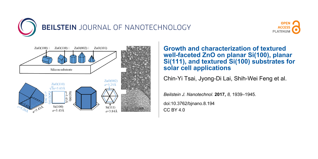
The exposed planes in the crystal growth process depend on both kinetic and thermodynamic factors, leading to a variety of structural morphologies [12]. The relationship between microstructure and crystal growth orientation of ZnO grown on silicon substrates is schematically illustrated in Figure 2 [12]. Here, the ZnO grains reveal a polygon structure for the c-axis parallel to the substrate, ridge-like structure, pyramid-like structure (hexagonal cylinder with or without the pyramidal tip), and pyramidal-tip without the hexagonal cylinder for ZnO(100), ZnO(110), ZnO(002), and ZnO(101) crystal planes, respectively.
![[2190-4286-8-194-2]](/bjnano/content/figures/2190-4286-8-194-2.png?scale=2.0&max-width=1024&background=FFFFFF)
Figure 2: Microstructure and crystal growth orientation of ZnO grown on silicon substrates. (a) ZnO(100) on the Si(111) substrate, a polygon structure with the c-axis growth parallel to the substrate; (b) ZnO(110) on the Si(100) substrate, a ZnO grain with a ridge-like structure; (c) ZnO(002) on the Si(111) substrate, a ZnO grain with a pyramid-like structure (hexagonal cylinder with or without a pyramidal tip); (d) ZnO(101) on the textured Si substrate, a ZnO grain with the pyramidal tip without a hexagonal cylinder.
Figure 2: Microstructure and crystal growth orientation of ZnO grown on silicon substrates. (a) ZnO(100) on t...
The surface morphologies shown in the SEM and AFM images for the three samples, shown in Figure 3 and Figure 4, respectively, can be explained by the above descriptions. The SEM images show that the ZnOp(100) sample has more ridge-like structures, while the ZnOp(111) sample has more pyramid-like structures. This result is consistent with the AFM images showing that the surface roughness of the ZnOp(100) sample is sharper than that of the ZnOp(111) sample. In addition, as shown in Table 1, the results of XRD, SEM, and AFM certainly indicate that, for the ZnOp(100) sample, the dominant ZnO(110) grains show ridge-like structures on the surface; for the ZnOp(111) sample, the dominant ZnO(002) grains show pyramid-like structures on the surface. For the ZnOt(100) sample, the dominant ZnO(101) grains show pyramidal tips without the hexagonal cylinder on the surface.
![[2190-4286-8-194-3]](/bjnano/content/figures/2190-4286-8-194-3.png?scale=2.0&max-width=1024&background=FFFFFF)
Figure 3: SEM images of the samples (a) ZnOp(100), (b) ZnOp(111), and (c) ZnOt(100).
Figure 3: SEM images of the samples (a) ZnOp(100), (b) ZnOp(111), and (c) ZnOt(100).
![[2190-4286-8-194-4]](/bjnano/content/figures/2190-4286-8-194-4.png?scale=2.0&max-width=1024&background=FFFFFF)
Figure 4: AFM images (5 × 5 μm) of the samples (a) ZnOp(100) (Rq: 48.488 nm), (b) ZnOp(111) (Rq: 48.284 nm), and (c) ZnOt(100). Surface roughness of each sample, Rq, is given in parentheses when available.
Figure 4: AFM images (5 × 5 μm) of the samples (a) ZnOp(100) (Rq: 48.488 nm), (b) ZnOp(111) (Rq: 48.284 nm), ...
Table 1: Main grain, surface morphology, surface roughness (Rq) from AFM, average grain size (D), strain (ε), and cathode luminescence (CL) intensity of the samples ZnOp(100), ZnOp(111), and ZnOt(100).
| Sample | Main grain | Surface morphology | Rq (nm) | D (nm) | ε | CL intensity |
|---|---|---|---|---|---|---|
| ZnOp(100) | ZnO(110) | ridge-like structure | 48.488 | 28.15 | 0.256 | stronger |
| ZnOp(111) | ZnO(002) | pyramid-like structure | 48.284 | 26.51 | 0.260 | medium |
| ZnOt(100) | ZnO(101) | pyramid-tip structure | – | 21.56 | 0.32 | weaker |
The microstructure and crystal growth orientation of ZnO grown on different silicon substrates can be explained by the lattice mismatch between the ZnO and silicon unit cells [16]. As schematically illustrated in Figure 5a, the surface of a Si(100) cubic unit cell is a square of 5.43 Å by 5.43Å which closely matches the rectangular surface of a ZnO(110) unit cell of 5.63 Å (![[Graphic 1]](/bjnano/content/inline/2190-4286-8-194-i3.svg?max-width=637&scale=1.18182) × lattice constant a) by 5.20 Å (lattice constant c). In Figure 5b, the surface of a Si(111) unit cell is a triangle of 3.84 Å. Six of these triangles form a hexagonal with sides of 3.84 Å, which closely matches the hexagonal surface of a ZnO(002) unit cell with 3.25 Å sides. It should be noted that the textured Si(100) substrate will in fact expose the Si(111) surface to form pyramid structures. However, the additional strain constraints from these Si surface textures will normally limit the growth of the ZnO(002) hexagonal cylinder and therefore favor the growth of the ZnO(101) pyramidal tips, with the same size of a surface unit cell as the ZnO(002), which closely match the textured silicon surface as well.
× lattice constant a) by 5.20 Å (lattice constant c). In Figure 5b, the surface of a Si(111) unit cell is a triangle of 3.84 Å. Six of these triangles form a hexagonal with sides of 3.84 Å, which closely matches the hexagonal surface of a ZnO(002) unit cell with 3.25 Å sides. It should be noted that the textured Si(100) substrate will in fact expose the Si(111) surface to form pyramid structures. However, the additional strain constraints from these Si surface textures will normally limit the growth of the ZnO(002) hexagonal cylinder and therefore favor the growth of the ZnO(101) pyramidal tips, with the same size of a surface unit cell as the ZnO(002), which closely match the textured silicon surface as well.
![[2190-4286-8-194-5]](/bjnano/content/figures/2190-4286-8-194-5.png?scale=2.0&max-width=1024&background=FFFFFF)
Figure 5:
(a) The lattice mismatch between a ZnO(110) unit cell of 5.63 Å (![[Graphic 2]](/bjnano/content/inline/2190-4286-8-194-i4.svg?max-width=637&scale=1.18182) × lattice constant a) by 5.20 Å (lattice constant c) and a Si(100) cubic unit cell of 5.43 Å by 5.43 Å; (b) the lattice mismatch between a hexagonal surface of a ZnO(002) unit cell with 3.25 Å sides and a hexagonal surface of six Si(111) triangular unit cells with 3.84 Å sides.
× lattice constant a) by 5.20 Å (lattice constant c) and a Si(100) cubic unit cell of 5.43 Å by 5.43 Å; (b) the lattice mismatch between a hexagonal surface of a ZnO(002) unit cell with 3.25 Å sides and a hexagonal surface of six Si(111) triangular unit cells with 3.84 Å sides.
Figure 5:
(a) The lattice mismatch between a ZnO(110) unit cell of 5.63 Å (× lattice constant a) by 5.20 Å (l...
As a result, the planar Si(100) substrate will favor ZnO(110) crystallization, while the planar Si(111) substrate will favor Zn(002). The surface morphology of the ZnO film on planar Si(100) substrate will have more ridge-like structures from the ZnO(110) grains, while the ZnO film on planar Si(111) substrate will have more pyramid-like structures from the ZnO(002) grains.
Average grain size and strain
In addition, the ZnO average grain size (D) can be calculated from the following equation [17]:
![[2190-4286-8-194-i1]](/bjnano/content/inline/2190-4286-8-194-i1.svg?max-width=590&scale=1.18182)
where βhkl, κ, λ, and θ are full width at half maximum (FWHM), shape factor (0.9), X-ray wavelength, and XRD angle, respectively. The results are shown in Figure 6a, which show that the D of the ZnOp(100) sample is slightly larger than that of the ZnOp(111) sample, while both of them are much larger than that of the ZnOt(100) sample. These results can also be consistently verified by the SEM images, which show that the surface granular textures on the ZnOp(100) sample are slightly larger than those on the ZnOp(111) sample, while both of them are much larger than those on the ZnOt(100) sample.
![[2190-4286-8-194-6]](/bjnano/content/figures/2190-4286-8-194-6.png?scale=2.0&max-width=1024&background=FFFFFF)
Figure 6: (a) Average grain size versus strain and (b) average grain size versus cathode luminescence (CL) intensity of the samples ZnOp(100), ZnOp(111), and ZnOt(100).
Figure 6: (a) Average grain size versus strain and (b) average grain size versus cathode luminescence (CL) in...
The XRD data can be analyzed to obtain not only the percentages of different grain crystal orientations but also the associated strain. The strain (ε) associated with the XRD peaks can be calculated by the following equation [17]:
![[2190-4286-8-194-i2]](/bjnano/content/inline/2190-4286-8-194-i2.svg?max-width=590&scale=1.18182)
where βhkl and θ are the FWHM and XRD angle, respectively. As shown in Figure 6a, the ε in the ZnOp(100) sample is slightly smaller than that in the ZnOp(111) sample, while both are much smaller than that in the ZnOt(100) sample. The average ZnO grain sizes grown on different silicon substrates decrease with increasing strains.
Cathode luminescence spectra
In addition, the average ZnO grain size can be indirectly verified from the results of the CL measurements of the three samples at room temperature (RT), as shown in Figure 7. The ZnO films are grown to be roughly the same thickness of 1.7 μm for the three different substrates. As a result, the measured CL intensity should be proportional to the degree of crystallization of ZnO grains. An emission peak around 378 nm (3.28 eV) is related to a band-to-band transition [4,5]. The CL intensity of the sample ZnOp(100) is stronger than that of the sample ZnOp(111), while both of them are much stronger than that of the sample ZnOt(100). Since a larger grain size corresponds to more crystalline structures and thus less defects, and this implies therefore stronger CL peak intensity, it can be expected that CL intensity is linearly proportional to the associated average grain size. As shown in Figure 6b, the average ZnO grain size estimated from XRD almost fully agrees with the CL intensity.
![[2190-4286-8-194-7]](/bjnano/content/figures/2190-4286-8-194-7.png?scale=2.0&max-width=1024&background=FFFFFF)
Figure 7: Cathode luminescence spectra of the samples (a) ZnOp(100), (b) ZnOp(111), and (c) ZnOt(100) with the excitations of 5, 7, 9, and 11 kV electron voltages at room temperature.
Figure 7: Cathode luminescence spectra of the samples (a) ZnOp(100), (b) ZnOp(111), and (c) ZnOt(100) with th...
Reflectance spectra
The reflectance spectra of the three samples were measured, as shown in Figure 8. It shows that the difference in the reflectance spectra between the ZnOp(100) and ZnOp(111) samples is insignificant. The ZnOt(100) sample has smaller reflectance due to the additional texture provided by the micrometer-sized pyramid structure of the texture Si(100) substrate. Therefore, it could be concluded that the antireflection function provided by theses samples mostly results from the nanometer-sized texture of the ZnO films while the micrometer-sized texture of the Si substrate has a limited contribution.
![[2190-4286-8-194-8]](/bjnano/content/figures/2190-4286-8-194-8.png?scale=2.0&max-width=1024&background=FFFFFF)
Figure 8: Reflectance spectra of the samples (a) ZnOp(100), (b) ZnOp(111), and (c) ZnOt(100) at room temperature.
Figure 8: Reflectance spectra of the samples (a) ZnOp(100), (b) ZnOp(111), and (c) ZnOt(100) at room temperat...
Discussion
The main grain orientation, surface morphology, AFM surface roughness (Rq) from AFM, average grain size (D), strain (ε), and CL intensity of samples ZnOp(100), ZnOp(111), and ZnOt(100) are shown in Table 1. The results clearly demonstrated that these results strongly agree the measurements from the SEM, AFM, and CL as well.
The results of this work show that the ZnO grown on the three different Si substrates all have stable granular structures with average grain size of 10–50 nm. Of course, in order to apply the ZnO thin films for applications in silicon solar cells, the defects resulting from the ZnO grains must be as minimal as possible. These results certainly imply that in order to minimize the defects of ZnO grains, the ZnO grain size should be as high as possible. It is worth noting that the ZnO samples grown on silicon substrates presented in this work have the potential to be a cost-effective alternative material for the substitution of the indium tin oxide (ITO) thin layer in heterojunction with intrinsic thin layer (HIT) solar cells [18]. Nevertheless, the optimization of the LPCVD growth conditions and parameters to increase the ZnO grain size and minimize their associated defects is an interesting issue for further studies and investigations.
Conclusion
In this work, textured and well-faceted ZnO samples are grown on planar Si(100), planar Si(111), and textured Si(100) substrates by the LPCVD method. Due to the constraints of the lattice mismatch between the ZnO and Si crystal structures, the ZnOp(100), ZnOp(111), and ZnOt(100) samples favor the growth of ZnO(110) ridge-like, ZnO(002) pyramid-like, and ZnO(101) pyramidal-tip structures, respectively. The average ZnO grain size on the planar Si(100) substrate is slightly larger than that on the planar Si(111) substrate, while both of them are much larger than that on the textured Si(100) substrate. It has been shown that the average grain sizes of ZnO grown on the different silicon substrates decrease due to the increases in the corresponding strain. Although this particular research result is not new, this work indeed provides useful information for optimized growth of textured and well-faceted ZnO grown on wafer-based silicon solar cells. These results can be utilized for efficiency enhancement by optimizing device structures, such as HIT solar cells, where the ZnO could be a cost-effective alternative material for ITO.
Experimental
Synthesis of ZnO on silicon substrates by LPCVD
Three different Si substrates, planar (100), planar (111), and textured (100), were prepared. These Si substrates were dipped in 5% HF solution to remove the native oxide layer and then rinsed in deionized water in 3 min. The ZnO films with the thickness of 1.7 μm were deposited on planar (100), planar (111), and textured (100) Si substrates (simply denoted as samples ZnOp(100), ZnOp(111), and ZnOt(100), respectively) at a temperature of 170 °C by a LPCVD process. Diethylzinc (DEZ) and water (H2O) vapors carried by argon gas were used as precursors, and their flow rates were set to 500 and 550 sccm, respectively. The textured Si(100) substrate was prepared from a monocrystalline Si(100) wafer anisotropically etched in NaOH/IPA solution at 85 °C to form pyramidal structures at the wafer surface. The surface roughness of these pyramidal structures was measured as 0.226 µm using AFM. Therefore, the average size of the pyramidal structures was taken to be approximately this value. The pyramidal structures will expose their (111) facets to the wafer surface. However, their physical properties for the LPCVD growth the ZnO films will be different from the (111) facets of the planar Si(111) substrate due to their different surface morphologies, especially, the additional strain introduced for ZnO films at the peaks and valleys of the pyramidal structures.
Characterization
The structures of the samples ZnOp(100), ZnOp(111), and ZnOt(100) were investigated with a high-resolution XRD (Bede D1). The surface morphology was revealed by atomic force microscopy (Park Systems, XE-70) operating in non-contact mode using a silicon tip of curvature less than 10 nm. Scanning electron microscope and cathode luminescence results were acquired by the use of a Gatan monoCL3 spectrometer in a JEOL JSM 7000F SEM system.
References
-
Morkoç, H.; Özgür, Ü. Zinc Oxide: Fundamentals, Materials and Device Technology; Wiley-VCH: Weinheim, Germany, 2007. doi:10.1002/9783527623945
Return to citation in text: [1] -
Özgür, Ü.; Alivov, Ya. I.; Liu, C.; Teke, A.; Reshchikov, M. A.; Doğan, S.; Avrutin, V.; Cho, S.-J.; Morkoç, H. J. Appl. Phys. 2005, 98, 041301. doi:10.1063/1.1992666
Return to citation in text: [1] -
Steinhauser, J. Low pressure chemical vapor deposited Zinc Oxide for thin film silicon solar cells. Ph.D. Thesis, University de Neuchâtel, Switzerland, 2008.
Return to citation in text: [1] [2] [3] [4] -
Lai, C.-M.; Huang, Y.-E.; Kou, K.-Y.; Chen, C.-H.; Tu, L.-W.; Feng, S.-W. Appl. Phys. Lett. 2015, 107, 022110. doi:10.1063/1.4926978
Return to citation in text: [1] [2] -
Kou, K.-Y.; Huang, Y.-E.; Chen, C.-H.; Feng, S.-W. Beilstein J. Nanotechnol. 2016, 7, 75–80. doi:10.3762/bjnano.7.9
Return to citation in text: [1] [2] -
Chen, X.-l.; Liu, J.-m.; Ni, J.; Zhao, Y.; Zhang, X.-d. Appl. Surf. Sci. 2015, 328, 193–197. doi:10.1016/j.apsusc.2014.12.018
Return to citation in text: [1] -
Shin, S. W.; Kim, I. Y.; Lee, G. H.; Agawane, G. L.; Mohokar, A. V.; Heo, G.-S.; Kim, J. H.; Lee, J. Y. Cryst. Growth Des. 2011, 11, 4819–4824. doi:10.1021/cg2005387
Return to citation in text: [1] -
Bikowski, A.; Ellmer, K. J. Mater. Res. 2012, 27, 2249–2256. doi:10.1557/jmr.2012.113
Return to citation in text: [1] -
Slassi, A.; Ziat, Y.; Zarhri, Z.; Abdellaoui, M.; Fakhim Lamrani, A. Phys. Scr. 2015, 90, 085801. doi:10.1088/0031-8949/90/8/085801
Return to citation in text: [1] -
Ellmer, K.; Klein, A.; Rech, B. Transparent Conductive Zinc Oxide: Basics and Applications in Thin Film Solar Cells; Springer: Berlin, Germany, 2008. doi:10.1007/978-3-540-73612-7
Return to citation in text: [1] -
Hu, Y.-H.; Chen, Y.-C.; Xu, H.-J.; Gao, H.; Jiang, W.-H.; Hu, F.; Wang, Y.-X. Engineering (Irvine, CA, U. S.) 2010, 2, 973–978. doi:10.4236/eng.2010.212124
Return to citation in text: [1] [2] [3] -
Shinagawa, T.; Shibata, K.; Shimomura, O.; Chigane, M.; Nomura, R.; Izaki, M. J. Mater. Chem. C 2014, 2, 2908–2917. doi:10.1039/C3TC32413C
Return to citation in text: [1] [2] [3] [4] -
Zhou, X.; Xie, Z.-X.; Jiang, Z.-Y.; Kuang, Q.; Zhang, S.-H.; Xu, T.; Huang, R.-B.; Zheng, L.-S. Chem. Commun. 2005, 44, 5572–5574. doi:10.1039/B510287A
Return to citation in text: [1] -
Liang, Y.-H.; Huang, J.-H.; Chang, N.-C.; Liu, C.-P. Cryst. Growth Des. 2009, 9, 2021–2025. doi:10.1021/cg8014018
Return to citation in text: [1] -
Warren, B. E. X-ray Diffraction; Dover Publications, Inc.: New York, NY, U.S.A., 1990.
Return to citation in text: [1] -
Fu, Z.; Lin, B.; Liao, G.; Wu, Z. J. Cryst. Growth 1998, 193, 316–321. doi:10.1016/S0022-0248(98)00511-9
Return to citation in text: [1] -
Mote, V. D.; Purushotham, Y.; Dole, B. N. J. Theor. Appl. Phys. 2012, 6, 6.
Return to citation in text: [1] [2] -
Mishima, T.; Taguchi, M.; Sakata, H.; Maruyama, E. Sol. Energ. Mat. Sol. Cells 2011, 95, 18–21. doi:10.1016/j.solmat.2010.04.030
Return to citation in text: [1]
| 18. | Mishima, T.; Taguchi, M.; Sakata, H.; Maruyama, E. Sol. Energ. Mat. Sol. Cells 2011, 95, 18–21. doi:10.1016/j.solmat.2010.04.030 |
| 1. | Morkoç, H.; Özgür, Ü. Zinc Oxide: Fundamentals, Materials and Device Technology; Wiley-VCH: Weinheim, Germany, 2007. doi:10.1002/9783527623945 |
| 2. | Özgür, Ü.; Alivov, Ya. I.; Liu, C.; Teke, A.; Reshchikov, M. A.; Doğan, S.; Avrutin, V.; Cho, S.-J.; Morkoç, H. J. Appl. Phys. 2005, 98, 041301. doi:10.1063/1.1992666 |
| 3. | Steinhauser, J. Low pressure chemical vapor deposited Zinc Oxide for thin film silicon solar cells. Ph.D. Thesis, University de Neuchâtel, Switzerland, 2008. |
| 4. | Lai, C.-M.; Huang, Y.-E.; Kou, K.-Y.; Chen, C.-H.; Tu, L.-W.; Feng, S.-W. Appl. Phys. Lett. 2015, 107, 022110. doi:10.1063/1.4926978 |
| 5. | Kou, K.-Y.; Huang, Y.-E.; Chen, C.-H.; Feng, S.-W. Beilstein J. Nanotechnol. 2016, 7, 75–80. doi:10.3762/bjnano.7.9 |
| 6. | Chen, X.-l.; Liu, J.-m.; Ni, J.; Zhao, Y.; Zhang, X.-d. Appl. Surf. Sci. 2015, 328, 193–197. doi:10.1016/j.apsusc.2014.12.018 |
| 7. | Shin, S. W.; Kim, I. Y.; Lee, G. H.; Agawane, G. L.; Mohokar, A. V.; Heo, G.-S.; Kim, J. H.; Lee, J. Y. Cryst. Growth Des. 2011, 11, 4819–4824. doi:10.1021/cg2005387 |
| 8. | Bikowski, A.; Ellmer, K. J. Mater. Res. 2012, 27, 2249–2256. doi:10.1557/jmr.2012.113 |
| 9. | Slassi, A.; Ziat, Y.; Zarhri, Z.; Abdellaoui, M.; Fakhim Lamrani, A. Phys. Scr. 2015, 90, 085801. doi:10.1088/0031-8949/90/8/085801 |
| 10. | Ellmer, K.; Klein, A.; Rech, B. Transparent Conductive Zinc Oxide: Basics and Applications in Thin Film Solar Cells; Springer: Berlin, Germany, 2008. doi:10.1007/978-3-540-73612-7 |
| 11. | Hu, Y.-H.; Chen, Y.-C.; Xu, H.-J.; Gao, H.; Jiang, W.-H.; Hu, F.; Wang, Y.-X. Engineering (Irvine, CA, U. S.) 2010, 2, 973–978. doi:10.4236/eng.2010.212124 |
| 12. | Shinagawa, T.; Shibata, K.; Shimomura, O.; Chigane, M.; Nomura, R.; Izaki, M. J. Mater. Chem. C 2014, 2, 2908–2917. doi:10.1039/C3TC32413C |
| 3. | Steinhauser, J. Low pressure chemical vapor deposited Zinc Oxide for thin film silicon solar cells. Ph.D. Thesis, University de Neuchâtel, Switzerland, 2008. |
| 4. | Lai, C.-M.; Huang, Y.-E.; Kou, K.-Y.; Chen, C.-H.; Tu, L.-W.; Feng, S.-W. Appl. Phys. Lett. 2015, 107, 022110. doi:10.1063/1.4926978 |
| 5. | Kou, K.-Y.; Huang, Y.-E.; Chen, C.-H.; Feng, S.-W. Beilstein J. Nanotechnol. 2016, 7, 75–80. doi:10.3762/bjnano.7.9 |
| 3. | Steinhauser, J. Low pressure chemical vapor deposited Zinc Oxide for thin film silicon solar cells. Ph.D. Thesis, University de Neuchâtel, Switzerland, 2008. |
| 16. | Fu, Z.; Lin, B.; Liao, G.; Wu, Z. J. Cryst. Growth 1998, 193, 316–321. doi:10.1016/S0022-0248(98)00511-9 |
| 3. | Steinhauser, J. Low pressure chemical vapor deposited Zinc Oxide for thin film silicon solar cells. Ph.D. Thesis, University de Neuchâtel, Switzerland, 2008. |
| 13. | Zhou, X.; Xie, Z.-X.; Jiang, Z.-Y.; Kuang, Q.; Zhang, S.-H.; Xu, T.; Huang, R.-B.; Zheng, L.-S. Chem. Commun. 2005, 44, 5572–5574. doi:10.1039/B510287A |
| 14. | Liang, Y.-H.; Huang, J.-H.; Chang, N.-C.; Liu, C.-P. Cryst. Growth Des. 2009, 9, 2021–2025. doi:10.1021/cg8014018 |
| 12. | Shinagawa, T.; Shibata, K.; Shimomura, O.; Chigane, M.; Nomura, R.; Izaki, M. J. Mater. Chem. C 2014, 2, 2908–2917. doi:10.1039/C3TC32413C |
| 12. | Shinagawa, T.; Shibata, K.; Shimomura, O.; Chigane, M.; Nomura, R.; Izaki, M. J. Mater. Chem. C 2014, 2, 2908–2917. doi:10.1039/C3TC32413C |
| 12. | Shinagawa, T.; Shibata, K.; Shimomura, O.; Chigane, M.; Nomura, R.; Izaki, M. J. Mater. Chem. C 2014, 2, 2908–2917. doi:10.1039/C3TC32413C |
| 11. | Hu, Y.-H.; Chen, Y.-C.; Xu, H.-J.; Gao, H.; Jiang, W.-H.; Hu, F.; Wang, Y.-X. Engineering (Irvine, CA, U. S.) 2010, 2, 973–978. doi:10.4236/eng.2010.212124 |
| 11. | Hu, Y.-H.; Chen, Y.-C.; Xu, H.-J.; Gao, H.; Jiang, W.-H.; Hu, F.; Wang, Y.-X. Engineering (Irvine, CA, U. S.) 2010, 2, 973–978. doi:10.4236/eng.2010.212124 |
| 15. | Warren, B. E. X-ray Diffraction; Dover Publications, Inc.: New York, NY, U.S.A., 1990. |
© 2017 Tsai et al.; licensee Beilstein-Institut.
This is an Open Access article under the terms of the Creative Commons Attribution License (http://creativecommons.org/licenses/by/4.0), which permits unrestricted use, distribution, and reproduction in any medium, provided the original work is properly cited.
The license is subject to the Beilstein Journal of Nanotechnology terms and conditions: (http://www.beilstein-journals.org/bjnano)