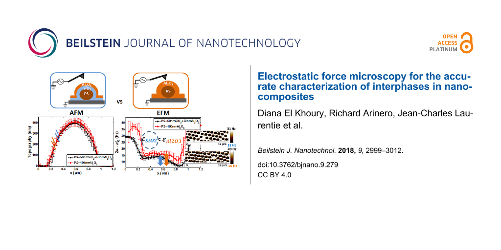
Abstract
The unusual properties of nanocomposites are commonly explained by the structure of their interphase. Therefore, these nanoscale interphase regions need to be precisely characterized; however, the existing high resolution experimental methods have not been reliably adapted to this purpose. Electrostatic force microscopy (EFM) represents a promising technique to fulfill this objective, although no complete and accurate interphase study has been published to date and EFM signal interpretation is not straightforward. The aim of this work was to establish accurate EFM signal analysis methods to investigate interphases in nanodielectrics using three experimental protocols. Samples with well-known, controllable properties were designed and synthesized to electrostatically model nanodielectrics with the aim of “calibrating” the EFM technique for future interphase studies. EFM was demonstrated to be able to discriminate between alumina and silicon dioxide interphase layers of 50 and 100 nm thickness deposited over polystyrene spheres and different types of matrix materials. Consistent permittivity values were also deduced by comparison of experimental data and numerical simulations, as well as the interface state of silicone dioxide layers.
Introduction
Composite nanomaterials (often referred to as “nanodielectrics” by the dielectrics community) can be synthesized by including dielectric nanoparticles in a polymeric matrix and are often used as insulating material [1-3]. Although the mechanical and thermal behavior of the base insulating polymer can be enhanced by microcomposites, its electrical performance is usually degraded [4,5]. On the other hand, the incorporation of nanofillers (1–10 wt %) into these polymers improves the dielectric properties of the resulting material, while meeting the thermal, mechanical and cost requirements [6-9].
This unusual behavior of nanocomposites is due to the interfacial region between the nanoparticles and polymer, also called the “interphase”. The interphase region can range from a few angstroms to a few nanometers, and usually has properties that differ from those of the polymer and filler. For instance, although the inorganic filler usually displays higher permittivity values than the polymer, the resulting nanofiller mixture in the matrix presents, at low nanofiller concentrations, a surprisingly lower dielectric constant than that of the two mixture components [10-13]. It is commonly agreed that the surface interaction of the nanoinclusions with the host polymer acts to rearrange the polymer chains and reduces their mobility at the interface [12-14]. The mobility reduction can lead to a decrease of the permittivity of the polar polymer, and consequently, also of the interphase. Moreover, it has been reported that water can be absorbed at the interface [15-17]. Water molecules within the interphase increase its effective dielectric constant, and this can explain the unexpectedly higher nanocomposite permittivity. Therefore, the local characterization of the interphase is of utmost importance to explain most of the nanocomposite macroscopic behavior, particularly their electrical polarization properties.
This local characterization requires high-resolution techniques that are sensitive to the dielectric properties of the material. These two conditions are fulfilled by electrostatic force microscopy (EFM) [18,19]. EFM is an atomic force microscopy (AFM)-based electrostatic method in which a conductive tip and a metallic sample holder are used. The probe-to-stage system is electrically polarized for the detection of electrostatic forces or force gradients. A proper interpretation of EFM results allows for the determination of the dielectric permittivity and dimensions of the sample components. Importantly, EFM is particularly suitable for electrical insulators, as opposed to electron microscopy where the rough specimen preparation procedures and electron beam bombardment can irreversibly electrically charge the material [20,21]. Moreover, while in the case of composites with 1D or 2D inclusions, the interphase can be directly accessed after cross-sectioning [20,21]; interphase characterization is more difficult for nanoparticle-filled materials. Indeed, the interphase is likely to be confined between the particles and the matrix below the probed region. Therefore, as the probing field is electrical in EFM, and this technology is expected to offer higher subsurface sensitivity compared with other scanning probe microscopy methods [22-25].
Subsurface imaging and 3D-multilayered structure studies with EFM have resulted in advances in our knowledge of specific types of materials. For instance, EFM comparison of the nanofiller diameter before and after insertion into the polymer matrix [26] showed an increase of the apparent particle diameter in the matrix that was attributed to the interphase. However, some experimental conditions during the comparison were not similar. Moreover, the highly probable presence of a matrix layer over the particles near the surface in the nanocomposite was ignored, although a matrix covering the nanoparticles would increase their apparent size even without an interphase. In a more rigorous study [27], Peng et al. detected, in sliced specimens of a nanodielectric, unexpectedly lower EFM signals above the filled matrix regions compared with the supposedly unfilled regions. To explain this EFM signal reduction, the authors hypothesized that an interphase with lower permittivity than that of particles and fillers surrounds the particles. However, the authors did not compare this remarkable change in local dielectric permittivity with macroscopic dielectric spectroscopy measurements. Nevertheless, the interphase characterization in nanocomposites is still inadequate. One common issue in these EFM-based works is that the exact source of the measured signal was not completely identified. Therefore, the measurement of complex materials remains a big challenge, mainly due to the complex geometry of the probe that scatters the electric field, and the long range nature of the electrostatic forces that complicate the identification of the actual probed region.
Therefore, the objectives of this study were to determine whether EFM can identify an interface region, and most importantly, to identify the appropriate experimental methods to extract the artifact-free EFM signal of the interphase. To this aim, materials of relatively known and modifiable composition and shape that electrostatically mimic a nanodielectric were designed and prepared to “calibrate” the technique. These were made of a stack of three dielectric constituents that represent a simplified configuration of the particle–interphase–matrix assembly found in nanodielectrics. Specifically, polystyrene (PS) nanoparticles of 380 nm diameter were prepared by self-assembly on metallized substrates. Then, two shells of variable thicknesses (50 and 100 nm) were deposited or grown over the whole sample surface. Aluminum oxide (Al2O3) shells were prepared using the atomic layer deposition (ALD) method, polyvinyl acetate (PVAc) shells by spin coating, and silicon dioxide (SiO2) shells by plasma sputtering deposition (PSD). The signature of each dielectric constituent was correlated to its dielectric permittivity. EFM measurements were performed using the double-pass method, while extracting the frequency shifts due to the acting electrostatic force gradients over the probe. During the second scan, the system was polarized at an AC voltage and the tip was retracted from the surface at a known distance, called the lift distance. At this stage, the component of the frequency shift that varies at the double frequency of the applied electrical voltage was extracted because it represents the purely capacitive response of the material. Finally, the experimental results were compared to finite element numerical simulations, obtained with the AC–DC module, electrostatics physics interface, of the Comsol® Multiphysics software.
Results and Discussion
In our previous work, we verified that EFM can distinguish homogeneous from heterogeneous stacked materials and provide information on the permittivity of their constituents relative to each other [28]. For instance, in materials made of particles with only one shell, the shell permittivity (εi) relative to that of the particle (εp) can be best obtained from signal comparisons at the center of the particles. Particularly, at a constant tip–sample distance, the signal increases with the thickness of the added material, and this can only be explained by an increase of the effective permittivity of the global material. This confirms the higher permittivity of the additional component compared with the initial one. Based on these findings, we developed three experimental approaches in which different model samples were compared to detect and characterize the interphase in a nanodielectric model composed of particle + interphase + matrix.
In all the tested model samples, the particle topography could be determined by a line scan because the covering layers were prepared in such a way to keep the curvature associated with the spheres. Completely embedded particles could also be used. However, the configuration where the particle protrudes from the surface has been described in previous works on interphases in “real” nanocomposite systems, using mechanical scanning probe microscopy techniques [29-31], and EFM [26,27,32,33]. Moreover, discriminating the particles from the topography is important in the case of nanocomposites that include particles and matrix with low dielectric permittivity difference.
Approach 1: PS + Al2O3 and PS + Al2O3 + PVAc
In the first method, the EFM signals for PS + 100 nm Al2O3 and PS + 100 nm Al2O3 + PVAc samples were compared (Figure 1). These samples mimicked a nanodielectric that has interphase (Al2O3) without and with a matrix surface layer, respectively.
![[2190-4286-9-279-1]](/bjnano/content/figures/2190-4286-9-279-1.png?scale=2.0&max-width=1024&background=FFFFFF)
Figure 1: Interphase detection, approach 1: schematic representation of the samples to be compared, and methodology.
Figure 1: Interphase detection, approach 1: schematic representation of the samples to be compared, and metho...
Al2O3 was the interphase model material to be detected, while PVAc (matrix) and PS (particle) were the known materials (depicted in Figure 1). As in the absence of interphase, εPVAc = 3.2 > εPS = 2.6, PVAc addition over the particles should increase the signal [34-36]. Conversely, in the presence of the Al2O3 interphase, alumina is supposed to enhance the effective permittivity of the covered particles and, consequently, PVAc addition should decrease the signal (i.e., interfacial effect due to the presence of a layer above the particles with higher permittivity compared with the PS + PVAc assembly). As changes in sample dimensions and permittivity values should be relatively small, the statistical analysis was performed using EFM measurements acquired on 12 × 3 µm2 images based on an average of 30 particles [37].
The calculated average topography and electrical frequency shift (2ω − Δf0) profiles for PS + 100 nm Al2O3 and PS + 100 nm Al2O3 + PVAc samples are presented in Figure 2a and 2b. The topography height was lower in samples with than in those without the matrix surface layer. Additional nanomechanical measurements indicated that this decrease was due to the non-uniformly thick spin-coated PVAc film [38]. In fact, as our samples were highly rough owing to the sub-micrometer PS spheres, spin-coating could not produce uniformly thin films [37]. However, this did not affect our study because the EFM results were compared at the center of the particles.
![[2190-4286-9-279-2]](/bjnano/content/figures/2190-4286-9-279-2.png?scale=2.0&max-width=1024&background=FFFFFF)
Figure 2: Approach 1 (PS + 100 nm Al2O3 and PS + 100 nm Al2O3 + PVAc samples): (a) average topography profiles, (b) average EFM signal profiles, and the corresponding AFM and EFM images (upper panels); tip–sample distance z ≈ 21 nm; reproduced with permission from [39], copyright 2018 IEEE.
Figure 2: Approach 1 (PS + 100 nm Al2O3 and PS + 100 nm Al2O3 + PVAc samples): (a) average topography profile...
Concerning the EFM signals, the average values calculated around the center were 20.6 ± 1.9 Hz for samples without matrix and 14.6 ± 1 Hz for samples with PVAc. This indicated that the matrix decreased the overall central signal by ≈30%, supporting our hypothesis on the effect of the Al2O3 interphase layer. This result confirmed the sensitivity of the first approach within the correct geometry and permittivity ratios in order to detect the region at the interface between PS particles and PVAc matrix. However, this methodology is limited by its concept based on comparing nanodielectrics with and without an upper matrix layer. Indeed, it is difficult to produce samples that lack a surface matrix layer without influencing the initial properties of the interphase. Therefore, it would be more realistic to compare samples that model nanodielectrics with and without an interphase.
Approach 2: PS + 50 nm SiO2 and PS + 100 nm Al2O3 + 50 nm SiO2
In the second approach, the comparison was between model nanodielectric samples without (PS + 50 nm SiO2) and with an interphase (PS + 100 nm Al2O3 + 50 nm SiO2) in which the matrix thickness was kept constant (Figure 3). To this aim, matrix deposition required a technique that allows the precise control of the thickness. For this reason, SiO2 was used instead of PVAc because it can be deposited by PSD. This method can precisely and homogeneously spread SiO2 molecules over the whole sample surface, quite similar to ALD, as explained in the Experimental section [40].
![[2190-4286-9-279-3]](/bjnano/content/figures/2190-4286-9-279-3.png?scale=2.0&max-width=1024&background=FFFFFF)
Figure 3: Interphase detection, approach 2: schematic representation of the samples to be compared, and methodology.
Figure 3: Interphase detection, approach 2: schematic representation of the samples to be compared, and metho...
In approach 2 (Figure 3), the signal between the compared samples should be similar in the absence of an interphase, whereas the Al2O3 interphase is expected to strengthen the signal, confirming the contribution of an additional layer with a higher permittivity than that of the PS + SiO2 sample. Indeed, as deduced from [28] and mentioned earlier, when the EFM signal increases in the presence of a thicker layer at the same tip–sample distance, this indicates that the added material possesses a dielectric permittivity higher than that of the initial particle + shell assembly. Although in our comparisons the added material was not at the surface but in the middle, the principle was the same [38].
A histogram illustrating the EFM signal distribution of PS + 50 nm SiO2 and PS + 100 nm Al2O3 + 50 nm SiO2 samples (Figure 4) showed the presence of two peaks. The maximum corresponded to the response from the bottom of the sample, and the lowest peak was the response from the particle center. A shift towards higher ∆f0 was observed for samples with the additional intermediate Al2O3 layer (arrow). This indicates that EFM can deduce the presence of an embedded Al2O3 interphase layer underneath the SiO2 matrix, and corroborates the hypothesis underlying this approach.
![[2190-4286-9-279-4]](/bjnano/content/figures/2190-4286-9-279-4.png?scale=2.0&max-width=1024&background=FFFFFF)
Figure 4: Approach 2: EFM images of PS + 50nmSiO2 (upper) and PS + 100 nm Al2O3 + 50 nm SiO2 (middle panel) samples, and their corresponding EFM signal distribution histogram (bottom); z = 21 nm.
Figure 4: Approach 2: EFM images of PS + 50nmSiO2 (upper) and PS + 100 nm Al2O3 + 50 nm SiO2 (middle panel) s...
This second approach is suitable to define the interphase relative dielectric permittivity, but only by comparison with that of the particle + matrix assembly. It can thus only indicate whether the interphase permittivity is higher or lower than the relative permittivity of the material with the highest permittivity (particle or matrix). Although such results are useful, the direct identification of the interphase, relative only to the matrix, is also essential. To this aim, a third method was evaluated.
Approach 3: comparisons of samples with similar dimensions
Like for approach 2, in approach 3, the comparison was between samples that model nanodielectrics with and without an interphase and in which the total shell thickness was kept constant. This removed any confusion due to the sample topography, and consequently the relative permittivity of the shell material became the prominent parameter. For this reason, approach 3 was divided in three steps outlined in Figure 5. In step A, the permittivity of the studied shells (Al2O3 and SiO2) was calibrated. In steps B and C, the Al2O3 interphase underneath (B) and covering (C) the SiO2 matrix was detected. If these materials behave normally, this approach should allow Al2O3 to be distinguished from SiO2 on the basis of the EFM signal increase, when it replaces it.
![[2190-4286-9-279-5]](/bjnano/content/figures/2190-4286-9-279-5.png?scale=2.0&max-width=1024&background=FFFFFF)
Figure 5: The three steps of approach 3: compared samples and methodologies.
Figure 5: The three steps of approach 3: compared samples and methodologies.
A tip–sample distance z of around 30.1 nm was kept for all measurements. The result reproducibility was always verified at several sample regions, and most of the time (in several comparable samples) measured with different probes. Since, as in this section, experimental data and simulations for a large set of samples were compared, only the results obtained with a specific probe will be presented.
Tip calibration
The first step to compare experimental data and simulations was to calibrate the tip geometry. One-point curves were performed using a metallic small-sized sample (10 nm × 2.5 nm), and the parabolic coefficient α2ω (Hz/V2) was calculated (please refer to Equation 7 in Experimental section). A tip radius of 28 nm and cone half-angle of 15º best fitted the experimental results, as indicated by the 4.6% total error compared with the simulations (Figure 6). Errors were measured as follows:
![[2190-4286-9-279-i1]](/bjnano/content/inline/2190-4286-9-279-i1.svg?max-width=590&scale=1.18182)
![[2190-4286-9-279-6]](/bjnano/content/figures/2190-4286-9-279-6.png?scale=2.0&max-width=1024&background=FFFFFF)
Figure 6: Tip calibration using the signal vs z curve. Experimental data fit simulations (tip radius of 29 nm and cone half-angle of 15º radius) with a total error of 4.6%.
Figure 6: Tip calibration using the signal vs z curve. Experimental data fit simulations (tip radius of 29 nm...
Reference polystyrene sample
The EFM and AFM images of the reference PS sample (Figure 7a,c) were used to extract the average topography and EFM cross-sectional profiles (Figure 7b,d). The average value of both profiles around the sample center was also calculated. The PS mean height was 383 ± 29 nm and the corresponding α2ω was 0.49 ± 0.07 Hz/V2. By implementing this PS geometry and experimental parameters in our numerical model, a PS dielectric permittivity of 2.6 was obtained that fit with the experimental data (0.08% error) (Table 1).
![[2190-4286-9-279-7]](/bjnano/content/figures/2190-4286-9-279-7.png?scale=2.0&max-width=1024&background=FFFFFF)
Figure 7: PS calibration – average cross-sectional profiles measured using a typical reference PS sample. (a) AFM image and (b) topography; (c) EFM image and (d) EFM response.
Figure 7: PS calibration – average cross-sectional profiles measured using a typical reference PS sample. (a)...
Table 1: Experimental data and simulations for a typical reference polystyrene sample, using z = 30.14 nm, tip-calibration parameters (28 nm, 15°), and average particle diameter = 382 nm. A particle permittivity of 2.6 fits simulations with 0.8% error.
| Experiment | Simulation | Comparison | ||
|---|---|---|---|---|
| α2ω (Hz/V2) | α2ω (Hz/V2) | ε | Error (%) | |
| Polystyrene | 0.49 ± 0.07 | 0.49 | 2.60 | 0.80 |
Step A: PS + 100 nm Al2O3 and PS + 100 nm SiO2 (shell calibration)
In step A (Figure 5 – shell calibration), the average topography profiles obtained by AFM image analysis (Figure 8a) between PS + 100 nm Al2O3 and PS + 100 nm SiO2 samples were comparable, as expected from the calibrated preparation process. Conversely, the average EFM profiles of the same samples (Figure 8b), also presented in the images of Figure 8 upper panel, were different in terms of signal magnitude, at the center of the particles and also at the bottom regions. As our samples had similar thicknesses, this difference could be explained by the different SiO2 and Al2O3 dielectric permittivity values. However, surprisingly, the EFM signal was higher with SiO2 than with Al2O3, although the SiO2 permittivity is lower than that of Al2O3 (3.9 for SiO2 and 9.8 for Al2O3) [34,36,41]. As Al2O3 shells have already been well characterized in the previous sections and also in [28] and showed predictable performance, this abnormal dielectric response could be attributed to SiO2.
![[2190-4286-9-279-8]](/bjnano/content/figures/2190-4286-9-279-8.png?scale=2.0&max-width=1024&background=FFFFFF)
Figure 8: Approach 3 (step A) PS + 100 nm Al2O3 and PS + 100 nm SiO2 samples: (a) Average topography profiles, (b) average EFM signal profiles, and their corresponding EFM images (upper panels).
Figure 8: Approach 3 (step A) PS + 100 nm Al2O3 and PS + 100 nm SiO2 samples: (a) Average topography profiles...
In the subsequent step, we correlated the experimental results with the simulations to allow for the calculation of the apparent permittivity of the shells, particularly SiO2. PS was modeled with a permittivity of 2.6, deduced during the calibration process (Table 1). For Al2O3, the dielectric permittivity of 9.8 was in accordance with the experimental data (error = 3.2%), and also in agreement with the expected Al2O3 behavior. Errors below 5% are widely acceptable, considering the errors related to tip and sphere calibration, film thicknesses, and the inherent experimental errors. The agreement between experimental data and simulations may also indicate that there is no additional interfacial effect between the particle and the shell, or at least, no dominant effect at this level of the material dimensions and properties. On the other hand, for SiO2, an apparent permittivity of εapp = 17 best fits the experimental data with an error of 0.6%. This permittivity was much higher than the usual SiO2 permittivity value (around 3.9). Consequently, step B and C measurements were performed by taking into account these values.
Step B: PS + 50 nm Al2O3 + 50 nm SiO2 and PS + 100 nm SiO2 (Al2O3 interphase detection)
After the validation of the deposition of similarly thick layers by ALD (Al2O3) and PSD (SiO2) and the calibration of the SiO2 and Al2O3 layers, stacking layers of SiO2 or Al2O3 over PS for detecting the intermediate material becomes relevant. The second main step aimed for addressing the interphase detection by comparing the EFM response of PS + 50 nm Al2O3 + 50 nm SiO2 and PS + 100 nm SiO2 samples. In this model, the interphase layer was 50 nm Al2O3 (Figure 5, step B).
Figure 9 shows that the average topography profiles of PS + 50 nm Al2O3 + 50 nm SiO2 and PS + 100 nm SiO2 samples were similar. Conversely, analysis of the EFM average response of Figure 9 upper panels indicated that the signal around the center decreased in samples with an intermediate Al2O3 layer (Figure 9b), as shown also by comparison of the mean values around the center (Table 2). This indicated the presence of an interphase effect. Moreover, the signal decrease with the Al2O3 interphase confirmed that its apparent permittivity was lower than that of SiO2. The abnormal behavior of these two materials was in accordance with the results obtained in step A. In fact, when simulations were performed using permittivity values of 9.8 and 17 for Al2O3 and SiO2, respectively, the simulations matched the experimental data (see Table 2).
![[2190-4286-9-279-9]](/bjnano/content/figures/2190-4286-9-279-9.png?scale=2.0&max-width=1024&background=FFFFFF)
Figure 9: Approach 3 (step B) PS + 50 nm Al2O3 + 50 nm SiO2 and PS + 100 nm SiO2 samples: (a) Average topography profiles, (b) average EFM signal profiles (lower panel) and the corresponding EFM images (upper panels). To avoid border effects, the EFM cross-sections were collected slightly far from the center and this is reflected by the change of the apparent particle width on the EFM average profiles.
Figure 9: Approach 3 (step B) PS + 50 nm Al2O3 + 50 nm SiO2 and PS + 100 nm SiO2 samples: (a) Average topogra...
Table 2: Experimental data and simulations for PS + 50 nm Al2O3 + 50 nm SiO2 and PS + 100 nm SiO2. The Al2O3 subsurface layer had a dielectric permittivity value of 9.8 (error = 5%) for a calibrated SiO2 upper layer with an apparent permittivity value of 17 (step A).
| Signal | Permittivity | ||||
|---|---|---|---|---|---|
| Exp. (Hz/V2) | Sim. (Hz/V2) | Error (%) | εinterphase | εmatrix | |
| PS + 100 nm SiO2 | 2.29 ± 0.33 | 2.27 | 0.60 | εSiO2 = 17 | εSiO2 = 17 |
| PS + 50 nm Al2O3 + 50 nm SiO2 | 2.01 ± 0.18 | 2.11 | 5.10 | εAl2O3 = 9.8 | εSiO2 = 17 |
The relatively small difference between PS + 50 nm Al2O3 + 50 nm SiO2 and PS + 100 nm SiO2 signals can be explained by the thickness of the upper layer (50 nm) that limits the electric field penetration, and consequently, the effect of the subsurface layer on the signal [38,42]. Moreover, the high dielectric polarization response of the surface material also masks the response from the deeper parts. Besides, the difference between the deduced apparent permittivity of SiO2 (εapp = 17) and of Al2O3 (εAl2O3 = 9.8) was relatively low. Notably, high dielectric permittivity materials are known to be difficult to distinguish [43], even if their effective permittivity decreases when they are placed on a material with lower permittivity (εPS = 2.6 < 9.8 and 17). Moreover, the reduction in sample effective permittivity enhances the EFM sensitivity to the top film [38,44].
Step C: PS + 50 nm SiO2 + 50 nm Al2O3 and PS + 100 nm Al2O3 (SiO2 interphase detection)
In step C, the comparison concerned the EFM response of PS + 50 nm SiO2 + 50 nm Al2O3 and PS + 100 nm Al2O3 samples (Figure 5, step C).
As observed in step B, while the average topography profiles were comparable (Figure 10a), the average EFM profiles were different between PS + 50 nm SiO2 + 50 nm Al2O3 and PS + 100 nm Al2O3 samples of Figure 10 upper panels (Figure 10b). The average electrical signal clearly decreased both at the particle center and at the bare substrate regions in PS + 50 nm SiO2 + 50 nm Al2O3, where a layer of 50 nm SiO2 was added underneath the 50 nm Al2O3 layer, compared with PS + 100 nm Al2O3, where only a 100 nm Al2O3 layer covered the PS.
![[2190-4286-9-279-10]](/bjnano/content/figures/2190-4286-9-279-10.png?scale=2.0&max-width=1024&background=FFFFFF)
Figure 10: Approach 3 - Step C (PS + 50 nm SiO2 + 50 nm Al2O3 and PS + 100 nm Al2O3 samples). a) Average topography profiles, b) average EFM signal profiles (lower panel) and the corresponding EFM images (upper panels).
Figure 10: Approach 3 - Step C (PS + 50 nm SiO2 + 50 nm Al2O3 and PS + 100 nm Al2O3 samples). a) Average topog...
In steps A and B, the apparent dielectric permittivity of SiO2 was 17. If this permittivity were maintained also when SiO2 was used as interphase layer, the EFM signal for SiO2-filled samples should have been higher than that of PS + 100 nm Al2O3 samples. This was not observed in the experimental conditions (Figure 10b). Conversely, the experimental results can be understood when using the nominal intrinsic bulk permittivity of SiO2 (around 3.9, thus lower than Al2O3 permittivity: εAl2O3 = 9.8). This hypothesis was verified by simulations in which the SiO2 and Al2O3 permittivity values were set at 3.9 and 9.8, respectively (Table 3).
Table 3: Experimental data and simulations for PS + 50 nm SiO2 + 50 nm Al2O3 and PS + 100 nm Al2O3 samples. The subsurface SiO2 layer displays a dielectric permittivity value of 3.9 (error = 0.3%).
| Signal | Permittivity | ||||
|---|---|---|---|---|---|
| Exp. (Hz/V2) | Sim. (Hz/V2) | Error (%) | εinterphase | εmatrix | |
| PS + 100 nm Al2O3 | 1.71 ± 0.26 | 1.65 | 3.24 | εAl2O3 = 9.8 | εAl2O3 = 9.8 |
| PS + 50 nm SiO2 + 50 nm Al2O3 | 1.48 ± 0.17 | 1.48 | 0.27 | εSiO2 = 3.9 | εAl2O3 = 9.8 |
In conclusion, steps B and C of approach 3 confirmed that EFM can be employed to characterize interfacial layers with similar configurations as those of the samples under study. Moreover, these results highlighted variable behavior of SiO2.
Discussion on approach 3
As in all three steps (A, B and C), SiO2 was deposited using the same technique, intrinsic material changes (bulk SiO2) cannot explain the apparent SiO2 permittivity variations among the samples. Our experimental data indicate that the SiO2 permittivity is higher than the standard value when SiO2 is placed on the sample surface, but not when it is used as an interphase. As the experiments were performed under ambient conditions, and SiO2 is a highly hydrophilic material, it can be hypothesized that a thin water layer was adsorbed on the surface. The high dielectric polarizability and permittivity of water films could explain the higher effective permittivity of superficial SiO2. Along the same lines, the normal value of the SiO2 interphase (PS + 50 nm SiO2 + 50 nm Al2O3) could be linked to the presence of an Al2O3 layer on the surface of SiO2. Al2O3 was prepared by ALD operated at low vacuum (0.001 mbar) at 80 °C and left to acquire temperature and vacuum stability for about 40 minutes before starting its deposition. In these thermodynamic conditions, water molecules might evaporate and the 40 min interval before deposition should have been enough to allow H2O desorption [45].
Although both SiO2 and Al2O3 are considered highly hydrophilic materials [15,46], SiO2 seems to retain water molecules on its surface more readily than Al2O3, as observed in Figure 8, and as confirmed by measurements performed in a highly humid environment [38]. Indeed, in the presence of high humidity, only scanning over alumina-covered samples was possible. All used probes were fixed to the surface and were consequently crushed or became contaminated, requiring a tip change. As a water meniscus created between the tip and the surface in air environment can cause the sticking of the tip to the surface at low distances, layers that adsorb more water molecules are supposed to be responsible for greater attraction forces. Consequently, a water meniscus can cause dynamic imaging instabilities [47], and an important water adsorption/absorption could explain the surface status difference between Al2O3 and SiO2.
The apparently higher SiO2 hydrophilicity could be attributed to the chemistry of the surface states resulting from the deposition method. ALD is a smooth chemical vapor deposition technique, expected to leave hydroxide OH groups on the surface. Conversely, PSD might induce a more homogeneous ionic surface state; O− and O2− could be typically introduced due to the small amount of reactive oxygen gas that is added to the neutral argon gas during sputtering [48].
This result was also verified for superimposed planar films, as deduced from the bottom regions of the sample (Figure 9b). In [38], we also tested these findings on entirely planar samples. Nevertheless, these hypotheses on the SiO2 surface emphasize the need for better investigations.
Discussion on the application for “real” nanodielectrics
The ultimate aim of this work is to use the proposed methodologies for investigating interphases in real materials where the only known parameters are the mixture components. With real nanodielectrics, the first, obvious step will be to compare materials that show unpredictable properties at the macroscale, indicating the possibility of the presence of interfacial effects. To this aim, a simple approach, inspired by Peng et al. work [27], would be thinning the material into slices, starting with a thickness slightly larger than the particle diameter. At this stage, our method 3 could be implemented. In the case of particles with low permittivity, particles protruding at the surface can be positioned using the topography data. Hence, protrusions with similar dimensions can be compared between the selected specimens, and method 3 can allow the range of possible interphase thickness and permittivity values to be determined. Similarly, when using particles with high permittivity, this approach might allow for the detection of particles in the depth of the material by EFM measurements and also using a statistical approach. Thus, comparing signals between various materials can provide information on the interphase. A correlation with other scanning probe microscopy methods would be also beneficial, such as the nanomechanical techniques that are adapted to similar types of materials with complex geometry and constituents.
Conclusion
This work demonstrates the accurate detection of interphases in nanocomposites using three EFM-based experimental protocols employing reference samples. As EFM signals represent the synergy of several parameters, the interpretation of the results is not straightforward for the analysis of interfacial effects in nanocomposites. For this reason, in this study, EFM measurements were performed using reference samples with relatively controlled and known properties whereby the samples were prepared to electrostatically model a nanodielectric material with an interphase. In these samples, three types of dielectric materials, each with a specific dielectric permittivity, were assembled in the form of sub-micrometer particles covered by two thin shells that represent the interphase and the matrix in the “real” systems. The study of the signals above the central region of the particles at constant tip–sample distance confirmed that EFM can differentiate between Al2O3 and SiO2 interphase layers of 50 and 100 nm over PS particles (380 nm) and between different types of matrix layers (PVAc, SiO2 and Al2O3). Specifically, three approaches were developed to distinguish the specific signal of the interphase layers based on sample comparison with the following configurations: 1) nanodielectrics (or nanodielectric regions) with and without the upper matrix layer; 2) nanodielectrics with and without interphase, and constant upper matrix thickness, and 3) nanodielectrics with and without interphase, with constant total particle coverage. The quantification of the dielectric permittivity of the used materials, within all types of association, was possible by comparing experimental data and numerical simulations. This paper also discussed the possibility of using the developed approaches to distinguish the composition and dielectric properties of “unknown” interphases in “real” nanocomposites with 3D inclusions, as well as in other types of heterogeneous nanometric materials, with reduced ambiguity about the real origin of the measured signals.
Experimental
Samples
The materials were specifically designed and prepared for this study to produce an electrostatic model of a nanodielectric (particle + interphase + matrix). They were based on spherical PS particles deposited on a metallic substrate. Al2O3, SiO2 and PVAc were used to cover the particles and to mimic either the interphase layer or the matrix layer. The PS particle diameter was about 380 nm and the shell thickness was 50 or 100 nm.
Polystyrene deposition and diameter monitoring
PS particles (initial diameter = 1 µm) (Sigma-Aldrich, ref: 89904) were deposited on previously metallized silicon substrates (Si-Mat Silicon materials, ref: 1014G1007) using the self-assembly property of PS spheres [49-51]. In this work, a more precise experimental protocol than the one used in our previous work [28] was chosen to deposit the particles by spin coating [52,53]. The initial PS sphere solution was mixed with ethanol (1:1 ratio) and kept in an ultrasound bath for 1 min to ensure homogeneous dispersion. Then, 7 µL of this diluted solution was spread over the whole substrate surface just before spinning. Substrates were previously hydrophilized in O2 plasma (50 W, 0.001 mbar) for 2 min. The following program was used for the spinning process: a) 100 rpm for 15 s, b) 500 rpm for 30 s and 2000 rpm for 60 s, all with a ramp of 2000 rpm between steps. Then, the obtained films of PS particles were etched in a plasma reactor with O2 as the reactive gas. The samples were inserted in the reactor chamber and pumped to reach a vacuum of approximatively 0.011 mbar. O2 was then introduced using a needle valve, and the pressure was equilibrated to 0.6 mbar by adjusting the valve. After the equilibrium pressure was reached, a radio frequency power of 50 W at 0.15 A was applied until the desired diameter (around 380 nm after 16 min etching) was obtained [54].
Shells
Alumina thin layers: atomic layer deposition (ALD). The ALD method was used to grow Al2O3 layers on the nanoparticles [55,56]. ALD is a thin film deposition technique where the film thickness is precisely controlled at the atomic level [57]. The deposition is based on sequential chemical reactions between gas precursors and the material surface. After each cycle of one precursor, an inert gas is introduced to remove the remaining precursor and the resulting by-products. The deposition conditions were the same as in [28]. The final theoretical configuration of the samples was similar to that of the PS + Al2O3 sample depicted in Figure 1.
Polyvinyl acetate thin layers: spin coating. Spin-coating was used to deposit PVAc films on the surface of particles with or without a previous covering layer. A solution containing 0.25 mg PVAc was mixed with 5 mL of toluene (highly evaporating solvent) and stirred with a magnetic stirrer until no particulate was visible (around 30 min). The spinning program used for thin film deposition was: a) 100 rpm for 15 s, b) 500 rpm for 15 s, and c) 2000 rpm for 60 s, all with a ramp of 2000 rpm.
Silicon dioxide thin films: plasma sputter deposition (PSD). Silicon dioxide layers were deposited by plasma sputtering in a Plassys 450S reactor using a high purity SiO2 target source. The deposition regime included a preliminary exposure to 100 sccm argon plasma at 50 W for 20 s, while substrates and SiO2 target samples were screened. Then, the target shutter was opened, and a pre-sputtering step (15 sccm Ar and 0.8 sccm O2 plasma gas at 200 W) was maintained for 30 s. Next, the substrate planetary rotation was launched and shutters opened, thus allowing the deposition of the SiO2 film. The film thickness was determined by the exposure time to SiO2 sputtering. Different from ALD, here the spherical shape of PS particles might not allow SiO2 to completely cover the corners between the particles and substrate, although sputtered SiO2 molecules invade the whole deposition chamber. Therefore, the final geometry could slightly differ from the PS + SiO2 depiction in Figure 3.
EFM experiments
The samples were mainly studied with EFM, using a double pass method with AC electrical excitation mode, while detecting the force gradients that vary at the double frequency of the electrical bias [58]. The interaction between the EFM tip and an insulator is the combination of the capacitive force between induced charges on the electrodes due to the capacitance C relative to the probed region, and a coulombic force between the local surface charges qs (if present) and their image charges on the tip – qs [58,59]. The general equation of the electrostatic force F that describes these interactions is defined as follows:
![[2190-4286-9-279-i2]](/bjnano/content/inline/2190-4286-9-279-i2.svg?max-width=590&scale=1.18182)
where z is the distance between the tip apex and the sample surface, qt is the sum of all charges interacting with the surface static charges qs, and the total voltage difference ΔV is expressed as:
![[2190-4286-9-279-i3]](/bjnano/content/inline/2190-4286-9-279-i3.svg?max-width=590&scale=1.18182)
where VDC and VACsin(ωt) are the DC and AC externally applied voltages, respectively, and VCP is the contact potential difference; qt is expressed as follows:
![[2190-4286-9-279-i4]](/bjnano/content/inline/2190-4286-9-279-i4.svg?max-width=590&scale=1.18182)
where qDC = CVDC, qAC = CVACsin(ωt) and qCP = CVCP are the capacitive charges due to
VDC, VACsin(ωt) and VCP, respectively.
Consequently, the development of Equation 1 shows that the force, and hence, the force gradient G (Nm−1), can both be expressed as the sum of the DC, ω and 2ω components. While the force and force gradient detection methods can provide relatively similar information on the electrical properties of the sample, the force gradient detection method is expected to offer higher lateral resolution and sensitivity [60].
The component of the gradient varying at the double of the electrical potential gradient is the only purely capacitive part without the need of further treatment, and it is described as:
![[2190-4286-9-279-i5]](/bjnano/content/inline/2190-4286-9-279-i5.svg?max-width=590&scale=1.18182)
EFM measurements were performed under ambient air conditions with a commercial AFM (Bruker, previously Veeco, EnviroscopeTM). The probe consisted of a metal covered tip (µmasch: HQ:NSC18/Pt) supported by a cantilever electrically connected to a metallic sample holder and biased at an electrical potential.
AC-biased EFM (ω = 100π rad) was employed in the double-pass configuration, while exciting the probe at its first eigenmode f0 [58]. During the first scan, sample topography was extracted and collected on a first image using the tapping mode. For the second scan, the sensor was lifted by a known distance from the surface, the so-called “lift” distance, and controlled to follow the topography profile acquired during the first scan. An AC voltage was then applied between the probe and the sample holder. Furthermore, the mechanical oscillation amplitude was reduced to stay in the linear regime. The detected electrostatic force gradients reduced the effective spring constant of the probe, K (N/m), and therefore, modified its resonance frequency. Consequently, at a constant mechanical working frequency, these electric force gradients tended to modify the signal phase, as deduced from the resolution of the tip motion equation [58]. In our experiments, the resonance frequency shifts Δf0 were extracted during the second scan by maintaining the phase shift constant throughout the modification of the cantilever exciting frequency.
In the linear regime, Δf0 and G are related by the following equation [58]:
![[2190-4286-9-279-i6]](/bjnano/content/inline/2190-4286-9-279-i6.svg?max-width=590&scale=1.18182)
Basically, the G2ω component was measured using an access module with a lock-in amplifier (EG&G Instruments – Model 5302), locked at the double frequency of the AC-electrical excitation and an arbitrary function generator (Sony Tektronic – AFG310). A custom-made switching device was used to extract the 2ω component from the signal obtained during the second pass. A 5 V AC-voltage with 200π rad/s pulsation was fixed for all EFM measurements.
The results are presented either as frequency shifts (2ω − Δf0), or as the EFM parabolic coefficient α2ω (Hz/V2), where:
![[2190-4286-9-279-i7]](/bjnano/content/inline/2190-4286-9-279-i7.svg?max-width=590&scale=1.18182)
Numerical simulations
Numerical simulations were obtained using the Comsol® Multiphysics software to corroborate the experimental results and to quantify the permittivity of the sample components.
To model the force acting on the EFM probe, the AC–DC module (electrostatics physics interface) of the software was used [61]. The probe was modeled according to the geometry of the standard EFM tips (i.e., as a solid truncated cone of height H = 10 µm and half-angle θ = 10° with a spherical apex of radius R0 at its end), calibrated for each new tip [28,62,63]. The geometry of each sample was implemented according to the theoretically expected geometry on the basis of the preparation methods (see Figure 1) but it was also verified using the AFM topography results [63].
The thickness of the deposited shells was monitored by characterizing reference samples for each film. However, these samples were prepared over bare substrates. Ellipsometry, electron microscopy and profilometry were used to verify the agreement between the theoretical and the actual Al2O3, SiO2, and PVAc thickness [38].
2D axisymmetric dimensions were used in accordance with model symmetry when measuring the force at the top of the particle/interphase assembly. The probe was biased at 5 V in DC, while the substrate was grounded. Only the z component of the electrostatic force was studied, like in previous finite-element EFM models [64].
In our simulations, the purely capacitive DC signal (perfect insulators) was computed (Figure 11). Then, to correlate AC measurements with the simulations, the amplitude of the demodulated 2ω-frequency shift was measured during the experiments. This AC-2ω signal is equal to the half of the DC signal (please refer to the theoretical equations of the DC versus AC-2ω components in [58,65]). Hence, the DC simulation results were divided by a factor of 2 to obtain the corresponding AC-2ω simulation values and compare them to the experimental AC-2ω values.
![[2190-4286-9-279-11]](/bjnano/content/figures/2190-4286-9-279-11.png?scale=2.0&max-width=1024&background=FFFFFF)
Figure 11: Typical simulation of the electric field map obtained with a 2D axisymmetric model of the EFM tip and the PS + Al2O3 sample as a substrate.
Figure 11: Typical simulation of the electric field map obtained with a 2D axisymmetric model of the EFM tip a...
References
-
Lewis, T. J. IEEE Trans. Dielectr. Electr. Insul. 1994, 1, 812–825. doi:10.1109/94.326653
Return to citation in text: [1] -
Frechette, M. F.; Trudeau, M. L.; Alamdari, H. D.; Boily, S. IEEE Trans. Dielectr. Electr. Insul. 2004, 11, 808–818. doi:10.1109/tdei.2004.1349786
Return to citation in text: [1] -
Psarras, G. C. eXPRESS Polym. Lett. 2008, 2, 460. doi:10.3144/expresspolymlett.2008.55
Return to citation in text: [1] -
Mayoux, C. IEEE Trans. Dielectr. Electr. Insul. 2000, 7, 590–601. doi:10.1109/tdei.2000.879355
Return to citation in text: [1] -
Cao, Y.; Irwin, P. C.; Younsi, K. IEEE Trans. Dielectr. Electr. Insul. 2004, 11, 797–807. doi:10.1109/tdei.2004.1349785
Return to citation in text: [1] -
Lewis, T. J. IEEE Trans. Dielectr. Electr. Insul. 2004, 11, 739–753. doi:10.1109/tdei.2004.1349779
Return to citation in text: [1] -
Tanaka, T.; Kozako, M.; Fuse, N.; Ohki, Y. IEEE Trans. Dielectr. Electr. Insul. 2005, 12, 669–681. doi:10.1109/tdei.2005.1511092
Return to citation in text: [1] -
Nelson, J. K. In 2007 Electrical Insulation Conference and Electrical Manufacturing Expo, Oct 22–24, 2007; 2007; pp 229–235. doi:10.1109/eeic.2007.4562626
Return to citation in text: [1] -
Santos, S.; Verdaguer, A. Materials 2016, 9, 182. doi:10.3390/ma9030182
Return to citation in text: [1] -
Kochetov, R.; Andritsch, T.; Morshuis, P. H. F.; Smit, J. J. IEEE Trans. Dielectr. Electr. Insul. 2012, 19, 107–117. doi:10.1109/tdei.2012.6148508
Return to citation in text: [1] -
Preda, I. A. Modeling and characterization of nanocomposite materials using dielectric methods. Ph.D. Thesis, Université Montpellier 2, Montpellier, France, 2013.
Return to citation in text: [1] -
Andritsh, T. Epoxy based nanocomposites for high voltage DC applications - Synthesis, Dielectric Properties and Space Charge Dynamics. Ph.D. Thesis, TU Delft, Delft, Netherlands, 2010.
Return to citation in text: [1] [2] -
Nelson, J. K.; Hu, Y.; Thiticharoenpong, J. In 2003 Annual Report Conference on Electrical Insulation and Dielectric Phenomena, Oct 19–22, 2003; 2003; pp 719–722. doi:10.1109/ceidp.2003.1254955
Return to citation in text: [1] [2] -
Kochetov, R. Thermal and Electrical Properties of Nanocomposites, Including Material Processing. Ph.D. Thesis, TU Delft, Delft, Netherlands, 2012.
Return to citation in text: [1] -
Zou, C.; Fothergill, J. C.; Rowe, S. W. IEEE Trans. Dielectr. Electr. Insul. 2008, 15, 106–117. doi:10.1109/t-dei.2008.4446741
Return to citation in text: [1] [2] -
Zhang, C.; Stevens, G. C. IEEE Trans. Dielectr. Electr. Insul. 2008, 15, 606–617. doi:10.1109/tdei.2008.4483483
Return to citation in text: [1] -
Fabiani, D.; Montanari, G. C.; Testa, L. IEEE Trans. Dielectr. Electr. Insul. 2010, 17, 221–230. doi:10.1109/tdei.2010.5412021
Return to citation in text: [1] -
Martin, Y.; Williams, C. C.; Wickramasinghe, H. K. J. Appl. Phys. 1987, 61, 4723–4729. doi:10.1063/1.338807
Return to citation in text: [1] -
Martin, Y.; Abraham, D. W.; Wickramasinghe, H. K. Appl. Phys. Lett. 1988, 52, 1103–1105. doi:10.1063/1.99224
Return to citation in text: [1] -
Wu, Q.; Li, M.; Gu, Y.; Wang, S.; Zhang, Z. Chin. J. Aeronaut. 2015, 28, 1529–1538. doi:10.1016/j.cja.2015.05.005
Return to citation in text: [1] [2] -
Uribe, B. E. B.; Tarpani, J. R. Compos. Interfaces 2017, 24, 849–859. doi:10.1080/09276440.2017.1299428
Return to citation in text: [1] [2] -
Thompson, H. T.; Barroso-Bujans, F.; Herrero, J. G.; Reifenberger, R.; Raman, A. Nanotechnology 2013, 24, 135701. doi:10.1088/0957-4484/24/13/135701
Return to citation in text: [1] -
Cadena, M. J.; Sung, S. H.; Boudouris, B. W.; Reifenberger, R.; Raman, A. ACS Nano 2016, 10, 4062–4071. doi:10.1021/acsnano.5b06893
Return to citation in text: [1] -
Castañeda-Uribe, O. A.; Reifenberger, R.; Raman, A.; Avila, A. ACS Nano 2015, 9, 2938–2947. doi:10.1021/nn507019c
Return to citation in text: [1] -
Cadena, M. J.; Chen, Y.; Reifenberger, R. G.; Raman, A. Appl. Phys. Lett. 2017, 110, 123108. doi:10.1063/1.4977837
Return to citation in text: [1] -
Seiler, J.; Kindersberger, J. IEEE Trans. Dielectr. Electr. Insul. 2014, 21, 537–547. doi:10.1109/tdei.2013.004388
Return to citation in text: [1] [2] -
Peng, S.; Zeng, Q.; Yang, X.; Hu, J.; Qiu, X.; He, J. Sci. Rep. 2016, 6, 38978. doi:10.1038/srep38978
Return to citation in text: [1] [2] [3] -
El Khoury, D.; Fedorenko, V.; Castellon, J.; Bechelany, M.; Laurentie, J.-C.; Balme, S.; Fréchette, M.; Ramonda, M.; Arinero, R. Scanning 2017, 2017, 4198519. doi:10.1155/2017/4198519
Return to citation in text: [1] [2] [3] [4] [5] [6] -
Cheng, S.; Bocharova, V.; Belianinov, A.; Xiong, S.; Kisliuk, A.; Somnath, S.; Holt, A. P.; Ovchinnikova, O. S.; Jesse, S.; Martin, H.; Etampawala, T.; Dadmun, M.; Sokolov, A. P. Nano Lett. 2016, 16, 3630–3637. doi:10.1021/acs.nanolett.6b00766
Return to citation in text: [1] -
Lahoud-Dignat, N.; Hidayatullah, M. N.; Saysouk, F.; Locatelli, M. L.; Diaham, S. In 2016 IEEE International Conference on Dielectrics (ICD), Montpellier, France, July 3–7, 2016; 2016; pp 64–67. doi:10.1109/icd.2016.7547544
Return to citation in text: [1] -
Huang, H.; Dobryden, I.; Ihrner, N.; Johansson, M.; Ma, H.; Pan, J.; Claesson, P. M. J. Colloid Interface Sci. 2017, 494, 204–214. doi:10.1016/j.jcis.2017.01.096
Return to citation in text: [1] -
Deschler, J.; Seiler, J.; Kindersberger, J. IEEE Trans. Dielectr. Electr. Insul. 2017, 24, 1027–1037. doi:10.1109/tdei.2017.006387
Return to citation in text: [1] -
Borgani, R.; Pallon, L. K. H.; Hedenqvist, M. S.; Gedde, U. W.; Haviland, D. B. Nano Lett. 2016, 16, 5934–5937. doi:10.1021/acs.nanolett.6b02920
Return to citation in text: [1] -
Ahmad, Z. Polymer Dielectric Materials. In Dielectric Material; Silaghis, M. A., Ed.; InTech: Rijeka, Croatia, 2012. doi:10.5772/50638
Return to citation in text: [1] [2] -
Riedel, C.; Arinero, R.; Tordjeman, P.; Leveque, G.; Schwartz, G. A.; Alegria, A.; Colmenero, J. Phys. Rev. E 2010, 81, 010801. doi:10.1103/physreve.81.010801
Return to citation in text: [1] -
Fumagalli, L.; Esteban-Ferrer, D.; Cuervo, A.; Carrascosa, J. L.; Gomila, G. Nat. Mater. 2012, 11, 808–816. doi:10.1038/nmat3369
Return to citation in text: [1] [2] -
Hershcovitz, M.; Klein, I. E. Microelectron. Reliab. 1993, 33, 869–880. doi:10.1016/0026-2714(93)90260-6
Return to citation in text: [1] [2] -
El Khoury, D. Towards the use of Electrostatic Force Microscopy to study interphases in nanodielectric materials. Ph.D. Thesis, Université de Montpellier, Montpellier, France, 2017.
Return to citation in text: [1] [2] [3] [4] [5] [6] [7] -
El Khoury, D.; Arinero, R.; Bechelany, M.; Laurentie, J. C.; Ramonda, M.; Castellon, J. In International Conference on Dielectrics 2018, Budapest, July 1–5, 2018; .
Return to citation in text: [1] -
Kinbara, A.; Kusano, E.; Kondo, I. Vacuum 1998, 51, 475–478. doi:10.1016/s0042-207x(98)00237-1
Return to citation in text: [1] -
Barber, P.; Balasubramanian, S.; Anguchamy, Y.; Gong, S.; Wibowo, A.; Gao, H.; Ploehn, H.; Zur Loye, H.-C. Materials 2009, 2, 1697–1733. doi:10.3390/ma2041697
Return to citation in text: [1] -
Ebeling, D.; Eslami, B.; Solares, S. D. J. ACS Nano 2013, 7, 10387–10396. doi:10.1021/nn404845q
Return to citation in text: [1] -
Castellano-Hernández, E.; Sacha, G. M. Appl. Phys. Lett. 2012, 100, 023101. doi:10.1063/1.3675446
Return to citation in text: [1] -
Castellano-Hernández, E.; Moreno-Llorena, J.; Sáenz, J. J.; Sacha, G. M. J. Phys.: Condens. Matter 2012, 24, 155303. doi:10.1088/0953-8984/24/15/155303
Return to citation in text: [1] -
Yanagihara, H.; Yamashita, K.; Endo, A.; Daiguji, H. J. Phys. Chem. C 2013, 117, 21795–21802. doi:10.1021/jp405623p
Return to citation in text: [1] -
Hosier, I. L.; Praeger, M.; Vaughan, A. S.; Swingler, S. G. IEEE Trans. Nanotechnol. 2017, 16, 667–676. doi:10.1109/tnano.2017.2703982
Return to citation in text: [1] -
Aimé, J.-P.; Boisgard, R.; Ondarçuhu, T. Nanomeniscus Mechanical Properties. In Nanoscale Liquid Interfaces – Wetting, Patterning and Force Microscopy at the Molecular Scale; Ondarçuhu, T.; Aimé, J.-P., Eds.; Pan Stanford Publishing Pte Ltd.: Singapore, 2013.
Return to citation in text: [1] -
Bradley, J. W.; Welzel, T. Process Diagnostics. In Reactive Sputter Deposition; Depla, D.; Mahieus, S., Eds.; Springer: Berlin, Germany, 2008; pp 255–300. doi:10.1007/978-3-540-76664-3_8
Return to citation in text: [1] -
Sakamoto, S.; Philippe, L.; Bechelany, M.; Michler, J.; Asoh, H.; Ono, S. Nanotechnology 2008, 19, 405304. doi:10.1088/0957-4484/19/40/405304
Return to citation in text: [1] -
Bechelany, M.; Brodard, P.; Philippe, L.; Michler, J. Nanotechnology 2009, 20, 455302. doi:10.1088/0957-4484/20/45/455302
Return to citation in text: [1] -
Elias, J.; Utke, I.; Yoon, S.; Bechelany, M.; Weidenkaff, A.; Michler, J.; Philippe, L. Electrochim. Acta 2013, 110, 387–392. doi:10.1016/j.electacta.2013.04.168
Return to citation in text: [1] -
Shinde, S. S.; Park, S. J. Semicond. 2015, 36, 023001. doi:10.1088/1674-4926/36/2/023001
Return to citation in text: [1] -
Arutinov, G.; Brichkin, S. B.; Razumov, V. F. Nanotechnol. Russ. 2010, 5, 67–72. doi:10.1134/s1995078010010064
Return to citation in text: [1] -
Bechelany, M.; Berodier, E.; Maeder, X.; Schmitt, S.; Michler, J.; Phillippe, L. ACS Appl. Mater. Interfaces 2011, 3, 3866–3873. doi:10.1021/am200948p
Return to citation in text: [1] -
Marichy, C.; Bechelany, M.; Pinna, N. Adv. Mater. 2012, 24, 1017–1032. doi:10.1002/adma.201104129
Return to citation in text: [1] -
Viter, R.; Iatsunskyi, I.; Fedorenko, V.; Tumenas, S.; Balevicius, Z.; Ramanavicius, A.; Balme, S.; Kempiński, M.; Nowaczyk, G.; Jurga, S.; Bechelany, M. J. Phys. Chem. C 2016, 120, 5124–5132. doi:10.1021/acs.jpcc.5b12263
Return to citation in text: [1] -
Baitimirova, M.; Viter, R.; Andzane, J.; van der Lee, A.; Voiry, D.; Iatsunskyi, I.; Coy, E.; Mikoliunaite, L.; Tumenas, S.; Załęski, K.; Balevicius, Z.; Baleviciute, I.; Ramanaviciene, A.; Ramanavicius, A.; Jurga, S.; Erts, D.; Bechelany, M. J. Phys. Chem. C 2016, 120, 23716–23725. doi:10.1021/acs.jpcc.6b07221
Return to citation in text: [1] -
Girard, P.; Titkov, A. N. Electrostatic Force and Force Gradient Microscopy: Principles, Points of Interest and Application to Characterisation of Semiconductor Materials and Devices. In Applied Scanning Probe Methods II: Scanning Probe Microscopy Techniques; Bhushan, B.; Fuchs, H., Eds.; Springer: Berlin, Germany, 2006; pp 283–320. doi:10.1007/3-540-27453-7_9
Return to citation in text: [1] [2] [3] [4] [5] [6] -
El Khoury, D.; Arinero, R.; Laurentie, J. C.; Castellon, J. AIP Adv. 2016, 6, 035318. doi:10.1063/1.4944953
Return to citation in text: [1] -
Bhushan, B.; Fuchs, H., Eds. Applied Scanning Probe Methods II; NanoScience and Technology; Springer Berlin: Berlin, Germany, 2006. doi:10.1007/b139097
Return to citation in text: [1] -
Gomila, G.; Toset, J.; Fumagalli, L. J. Appl. Phys. 2008, 104, 024315. doi:10.1063/1.2957069
Return to citation in text: [1] -
Fumagalli, L.; Edwards, M. A.; Gomila, G. Nanotechnology 2014, 25, 495701. doi:10.1088/0957-4484/25/49/495701
Return to citation in text: [1] -
El Khoury, D.; Arinero, R.; Laurentie, J.-C.; Castellon, J.; Fréchette, M. In 2016 IEEE International Conference on Dielectrics (ICD), July 3–7, 2016; pp 800–803. doi:10.1109/icd.2016.7547737
Return to citation in text: [1] [2] -
Hudlet, S.; Saint Jean, M.; Guthmann, C.; Berger, J. Eur. Phys. J. B 1998, 2, 5–10. doi:10.1007/s100510050219
Return to citation in text: [1] -
Sarid, D. Scanning Force Microscopy with Applications to Electric, Magnetic and Atomic Forces; Oxford University Press: Oxford, United Kingdom, 1994.
Return to citation in text: [1]
| 38. | El Khoury, D. Towards the use of Electrostatic Force Microscopy to study interphases in nanodielectric materials. Ph.D. Thesis, Université de Montpellier, Montpellier, France, 2017. |
| 44. | Castellano-Hernández, E.; Moreno-Llorena, J.; Sáenz, J. J.; Sacha, G. M. J. Phys.: Condens. Matter 2012, 24, 155303. doi:10.1088/0953-8984/24/15/155303 |
| 45. | Yanagihara, H.; Yamashita, K.; Endo, A.; Daiguji, H. J. Phys. Chem. C 2013, 117, 21795–21802. doi:10.1021/jp405623p |
| 15. | Zou, C.; Fothergill, J. C.; Rowe, S. W. IEEE Trans. Dielectr. Electr. Insul. 2008, 15, 106–117. doi:10.1109/t-dei.2008.4446741 |
| 46. | Hosier, I. L.; Praeger, M.; Vaughan, A. S.; Swingler, S. G. IEEE Trans. Nanotechnol. 2017, 16, 667–676. doi:10.1109/tnano.2017.2703982 |
| 28. | El Khoury, D.; Fedorenko, V.; Castellon, J.; Bechelany, M.; Laurentie, J.-C.; Balme, S.; Fréchette, M.; Ramonda, M.; Arinero, R. Scanning 2017, 2017, 4198519. doi:10.1155/2017/4198519 |
| 52. | Shinde, S. S.; Park, S. J. Semicond. 2015, 36, 023001. doi:10.1088/1674-4926/36/2/023001 |
| 53. | Arutinov, G.; Brichkin, S. B.; Razumov, V. F. Nanotechnol. Russ. 2010, 5, 67–72. doi:10.1134/s1995078010010064 |
| 27. | Peng, S.; Zeng, Q.; Yang, X.; Hu, J.; Qiu, X.; He, J. Sci. Rep. 2016, 6, 38978. doi:10.1038/srep38978 |
| 49. | Sakamoto, S.; Philippe, L.; Bechelany, M.; Michler, J.; Asoh, H.; Ono, S. Nanotechnology 2008, 19, 405304. doi:10.1088/0957-4484/19/40/405304 |
| 50. | Bechelany, M.; Brodard, P.; Philippe, L.; Michler, J. Nanotechnology 2009, 20, 455302. doi:10.1088/0957-4484/20/45/455302 |
| 51. | Elias, J.; Utke, I.; Yoon, S.; Bechelany, M.; Weidenkaff, A.; Michler, J.; Philippe, L. Electrochim. Acta 2013, 110, 387–392. doi:10.1016/j.electacta.2013.04.168 |
| 48. | Bradley, J. W.; Welzel, T. Process Diagnostics. In Reactive Sputter Deposition; Depla, D.; Mahieus, S., Eds.; Springer: Berlin, Germany, 2008; pp 255–300. doi:10.1007/978-3-540-76664-3_8 |
| 38. | El Khoury, D. Towards the use of Electrostatic Force Microscopy to study interphases in nanodielectric materials. Ph.D. Thesis, Université de Montpellier, Montpellier, France, 2017. |
| 38. | El Khoury, D. Towards the use of Electrostatic Force Microscopy to study interphases in nanodielectric materials. Ph.D. Thesis, Université de Montpellier, Montpellier, France, 2017. |
| 47. | Aimé, J.-P.; Boisgard, R.; Ondarçuhu, T. Nanomeniscus Mechanical Properties. In Nanoscale Liquid Interfaces – Wetting, Patterning and Force Microscopy at the Molecular Scale; Ondarçuhu, T.; Aimé, J.-P., Eds.; Pan Stanford Publishing Pte Ltd.: Singapore, 2013. |
| 54. | Bechelany, M.; Berodier, E.; Maeder, X.; Schmitt, S.; Michler, J.; Phillippe, L. ACS Appl. Mater. Interfaces 2011, 3, 3866–3873. doi:10.1021/am200948p |
| 55. | Marichy, C.; Bechelany, M.; Pinna, N. Adv. Mater. 2012, 24, 1017–1032. doi:10.1002/adma.201104129 |
| 56. | Viter, R.; Iatsunskyi, I.; Fedorenko, V.; Tumenas, S.; Balevicius, Z.; Ramanavicius, A.; Balme, S.; Kempiński, M.; Nowaczyk, G.; Jurga, S.; Bechelany, M. J. Phys. Chem. C 2016, 120, 5124–5132. doi:10.1021/acs.jpcc.5b12263 |
| 57. | Baitimirova, M.; Viter, R.; Andzane, J.; van der Lee, A.; Voiry, D.; Iatsunskyi, I.; Coy, E.; Mikoliunaite, L.; Tumenas, S.; Załęski, K.; Balevicius, Z.; Baleviciute, I.; Ramanaviciene, A.; Ramanavicius, A.; Jurga, S.; Erts, D.; Bechelany, M. J. Phys. Chem. C 2016, 120, 23716–23725. doi:10.1021/acs.jpcc.6b07221 |
| 58. | Girard, P.; Titkov, A. N. Electrostatic Force and Force Gradient Microscopy: Principles, Points of Interest and Application to Characterisation of Semiconductor Materials and Devices. In Applied Scanning Probe Methods II: Scanning Probe Microscopy Techniques; Bhushan, B.; Fuchs, H., Eds.; Springer: Berlin, Germany, 2006; pp 283–320. doi:10.1007/3-540-27453-7_9 |
| 61. | Gomila, G.; Toset, J.; Fumagalli, L. J. Appl. Phys. 2008, 104, 024315. doi:10.1063/1.2957069 |
| 58. | Girard, P.; Titkov, A. N. Electrostatic Force and Force Gradient Microscopy: Principles, Points of Interest and Application to Characterisation of Semiconductor Materials and Devices. In Applied Scanning Probe Methods II: Scanning Probe Microscopy Techniques; Bhushan, B.; Fuchs, H., Eds.; Springer: Berlin, Germany, 2006; pp 283–320. doi:10.1007/3-540-27453-7_9 |
| 58. | Girard, P.; Titkov, A. N. Electrostatic Force and Force Gradient Microscopy: Principles, Points of Interest and Application to Characterisation of Semiconductor Materials and Devices. In Applied Scanning Probe Methods II: Scanning Probe Microscopy Techniques; Bhushan, B.; Fuchs, H., Eds.; Springer: Berlin, Germany, 2006; pp 283–320. doi:10.1007/3-540-27453-7_9 |
| 58. | Girard, P.; Titkov, A. N. Electrostatic Force and Force Gradient Microscopy: Principles, Points of Interest and Application to Characterisation of Semiconductor Materials and Devices. In Applied Scanning Probe Methods II: Scanning Probe Microscopy Techniques; Bhushan, B.; Fuchs, H., Eds.; Springer: Berlin, Germany, 2006; pp 283–320. doi:10.1007/3-540-27453-7_9 |
| 59. | El Khoury, D.; Arinero, R.; Laurentie, J. C.; Castellon, J. AIP Adv. 2016, 6, 035318. doi:10.1063/1.4944953 |
| 60. | Bhushan, B.; Fuchs, H., Eds. Applied Scanning Probe Methods II; NanoScience and Technology; Springer Berlin: Berlin, Germany, 2006. doi:10.1007/b139097 |
| 28. | El Khoury, D.; Fedorenko, V.; Castellon, J.; Bechelany, M.; Laurentie, J.-C.; Balme, S.; Fréchette, M.; Ramonda, M.; Arinero, R. Scanning 2017, 2017, 4198519. doi:10.1155/2017/4198519 |
| 58. | Girard, P.; Titkov, A. N. Electrostatic Force and Force Gradient Microscopy: Principles, Points of Interest and Application to Characterisation of Semiconductor Materials and Devices. In Applied Scanning Probe Methods II: Scanning Probe Microscopy Techniques; Bhushan, B.; Fuchs, H., Eds.; Springer: Berlin, Germany, 2006; pp 283–320. doi:10.1007/3-540-27453-7_9 |
| 63. | El Khoury, D.; Arinero, R.; Laurentie, J.-C.; Castellon, J.; Fréchette, M. In 2016 IEEE International Conference on Dielectrics (ICD), July 3–7, 2016; pp 800–803. doi:10.1109/icd.2016.7547737 |
| 38. | El Khoury, D. Towards the use of Electrostatic Force Microscopy to study interphases in nanodielectric materials. Ph.D. Thesis, Université de Montpellier, Montpellier, France, 2017. |
| 28. | El Khoury, D.; Fedorenko, V.; Castellon, J.; Bechelany, M.; Laurentie, J.-C.; Balme, S.; Fréchette, M.; Ramonda, M.; Arinero, R. Scanning 2017, 2017, 4198519. doi:10.1155/2017/4198519 |
| 62. | Fumagalli, L.; Edwards, M. A.; Gomila, G. Nanotechnology 2014, 25, 495701. doi:10.1088/0957-4484/25/49/495701 |
| 63. | El Khoury, D.; Arinero, R.; Laurentie, J.-C.; Castellon, J.; Fréchette, M. In 2016 IEEE International Conference on Dielectrics (ICD), July 3–7, 2016; pp 800–803. doi:10.1109/icd.2016.7547737 |
| 1. | Lewis, T. J. IEEE Trans. Dielectr. Electr. Insul. 1994, 1, 812–825. doi:10.1109/94.326653 |
| 2. | Frechette, M. F.; Trudeau, M. L.; Alamdari, H. D.; Boily, S. IEEE Trans. Dielectr. Electr. Insul. 2004, 11, 808–818. doi:10.1109/tdei.2004.1349786 |
| 3. | Psarras, G. C. eXPRESS Polym. Lett. 2008, 2, 460. doi:10.3144/expresspolymlett.2008.55 |
| 12. | Andritsh, T. Epoxy based nanocomposites for high voltage DC applications - Synthesis, Dielectric Properties and Space Charge Dynamics. Ph.D. Thesis, TU Delft, Delft, Netherlands, 2010. |
| 13. | Nelson, J. K.; Hu, Y.; Thiticharoenpong, J. In 2003 Annual Report Conference on Electrical Insulation and Dielectric Phenomena, Oct 19–22, 2003; 2003; pp 719–722. doi:10.1109/ceidp.2003.1254955 |
| 14. | Kochetov, R. Thermal and Electrical Properties of Nanocomposites, Including Material Processing. Ph.D. Thesis, TU Delft, Delft, Netherlands, 2012. |
| 26. | Seiler, J.; Kindersberger, J. IEEE Trans. Dielectr. Electr. Insul. 2014, 21, 537–547. doi:10.1109/tdei.2013.004388 |
| 27. | Peng, S.; Zeng, Q.; Yang, X.; Hu, J.; Qiu, X.; He, J. Sci. Rep. 2016, 6, 38978. doi:10.1038/srep38978 |
| 32. | Deschler, J.; Seiler, J.; Kindersberger, J. IEEE Trans. Dielectr. Electr. Insul. 2017, 24, 1027–1037. doi:10.1109/tdei.2017.006387 |
| 33. | Borgani, R.; Pallon, L. K. H.; Hedenqvist, M. S.; Gedde, U. W.; Haviland, D. B. Nano Lett. 2016, 16, 5934–5937. doi:10.1021/acs.nanolett.6b02920 |
| 10. | Kochetov, R.; Andritsch, T.; Morshuis, P. H. F.; Smit, J. J. IEEE Trans. Dielectr. Electr. Insul. 2012, 19, 107–117. doi:10.1109/tdei.2012.6148508 |
| 11. | Preda, I. A. Modeling and characterization of nanocomposite materials using dielectric methods. Ph.D. Thesis, Université Montpellier 2, Montpellier, France, 2013. |
| 12. | Andritsh, T. Epoxy based nanocomposites for high voltage DC applications - Synthesis, Dielectric Properties and Space Charge Dynamics. Ph.D. Thesis, TU Delft, Delft, Netherlands, 2010. |
| 13. | Nelson, J. K.; Hu, Y.; Thiticharoenpong, J. In 2003 Annual Report Conference on Electrical Insulation and Dielectric Phenomena, Oct 19–22, 2003; 2003; pp 719–722. doi:10.1109/ceidp.2003.1254955 |
| 34. | Ahmad, Z. Polymer Dielectric Materials. In Dielectric Material; Silaghis, M. A., Ed.; InTech: Rijeka, Croatia, 2012. doi:10.5772/50638 |
| 35. | Riedel, C.; Arinero, R.; Tordjeman, P.; Leveque, G.; Schwartz, G. A.; Alegria, A.; Colmenero, J. Phys. Rev. E 2010, 81, 010801. doi:10.1103/physreve.81.010801 |
| 36. | Fumagalli, L.; Esteban-Ferrer, D.; Cuervo, A.; Carrascosa, J. L.; Gomila, G. Nat. Mater. 2012, 11, 808–816. doi:10.1038/nmat3369 |
| 6. | Lewis, T. J. IEEE Trans. Dielectr. Electr. Insul. 2004, 11, 739–753. doi:10.1109/tdei.2004.1349779 |
| 7. | Tanaka, T.; Kozako, M.; Fuse, N.; Ohki, Y. IEEE Trans. Dielectr. Electr. Insul. 2005, 12, 669–681. doi:10.1109/tdei.2005.1511092 |
| 8. | Nelson, J. K. In 2007 Electrical Insulation Conference and Electrical Manufacturing Expo, Oct 22–24, 2007; 2007; pp 229–235. doi:10.1109/eeic.2007.4562626 |
| 9. | Santos, S.; Verdaguer, A. Materials 2016, 9, 182. doi:10.3390/ma9030182 |
| 28. | El Khoury, D.; Fedorenko, V.; Castellon, J.; Bechelany, M.; Laurentie, J.-C.; Balme, S.; Fréchette, M.; Ramonda, M.; Arinero, R. Scanning 2017, 2017, 4198519. doi:10.1155/2017/4198519 |
| 4. | Mayoux, C. IEEE Trans. Dielectr. Electr. Insul. 2000, 7, 590–601. doi:10.1109/tdei.2000.879355 |
| 5. | Cao, Y.; Irwin, P. C.; Younsi, K. IEEE Trans. Dielectr. Electr. Insul. 2004, 11, 797–807. doi:10.1109/tdei.2004.1349785 |
| 29. | Cheng, S.; Bocharova, V.; Belianinov, A.; Xiong, S.; Kisliuk, A.; Somnath, S.; Holt, A. P.; Ovchinnikova, O. S.; Jesse, S.; Martin, H.; Etampawala, T.; Dadmun, M.; Sokolov, A. P. Nano Lett. 2016, 16, 3630–3637. doi:10.1021/acs.nanolett.6b00766 |
| 30. | Lahoud-Dignat, N.; Hidayatullah, M. N.; Saysouk, F.; Locatelli, M. L.; Diaham, S. In 2016 IEEE International Conference on Dielectrics (ICD), Montpellier, France, July 3–7, 2016; 2016; pp 64–67. doi:10.1109/icd.2016.7547544 |
| 31. | Huang, H.; Dobryden, I.; Ihrner, N.; Johansson, M.; Ma, H.; Pan, J.; Claesson, P. M. J. Colloid Interface Sci. 2017, 494, 204–214. doi:10.1016/j.jcis.2017.01.096 |
| 20. | Wu, Q.; Li, M.; Gu, Y.; Wang, S.; Zhang, Z. Chin. J. Aeronaut. 2015, 28, 1529–1538. doi:10.1016/j.cja.2015.05.005 |
| 21. | Uribe, B. E. B.; Tarpani, J. R. Compos. Interfaces 2017, 24, 849–859. doi:10.1080/09276440.2017.1299428 |
| 26. | Seiler, J.; Kindersberger, J. IEEE Trans. Dielectr. Electr. Insul. 2014, 21, 537–547. doi:10.1109/tdei.2013.004388 |
| 20. | Wu, Q.; Li, M.; Gu, Y.; Wang, S.; Zhang, Z. Chin. J. Aeronaut. 2015, 28, 1529–1538. doi:10.1016/j.cja.2015.05.005 |
| 21. | Uribe, B. E. B.; Tarpani, J. R. Compos. Interfaces 2017, 24, 849–859. doi:10.1080/09276440.2017.1299428 |
| 27. | Peng, S.; Zeng, Q.; Yang, X.; Hu, J.; Qiu, X.; He, J. Sci. Rep. 2016, 6, 38978. doi:10.1038/srep38978 |
| 18. | Martin, Y.; Williams, C. C.; Wickramasinghe, H. K. J. Appl. Phys. 1987, 61, 4723–4729. doi:10.1063/1.338807 |
| 19. | Martin, Y.; Abraham, D. W.; Wickramasinghe, H. K. Appl. Phys. Lett. 1988, 52, 1103–1105. doi:10.1063/1.99224 |
| 64. | Hudlet, S.; Saint Jean, M.; Guthmann, C.; Berger, J. Eur. Phys. J. B 1998, 2, 5–10. doi:10.1007/s100510050219 |
| 15. | Zou, C.; Fothergill, J. C.; Rowe, S. W. IEEE Trans. Dielectr. Electr. Insul. 2008, 15, 106–117. doi:10.1109/t-dei.2008.4446741 |
| 16. | Zhang, C.; Stevens, G. C. IEEE Trans. Dielectr. Electr. Insul. 2008, 15, 606–617. doi:10.1109/tdei.2008.4483483 |
| 17. | Fabiani, D.; Montanari, G. C.; Testa, L. IEEE Trans. Dielectr. Electr. Insul. 2010, 17, 221–230. doi:10.1109/tdei.2010.5412021 |
| 22. | Thompson, H. T.; Barroso-Bujans, F.; Herrero, J. G.; Reifenberger, R.; Raman, A. Nanotechnology 2013, 24, 135701. doi:10.1088/0957-4484/24/13/135701 |
| 23. | Cadena, M. J.; Sung, S. H.; Boudouris, B. W.; Reifenberger, R.; Raman, A. ACS Nano 2016, 10, 4062–4071. doi:10.1021/acsnano.5b06893 |
| 24. | Castañeda-Uribe, O. A.; Reifenberger, R.; Raman, A.; Avila, A. ACS Nano 2015, 9, 2938–2947. doi:10.1021/nn507019c |
| 25. | Cadena, M. J.; Chen, Y.; Reifenberger, R. G.; Raman, A. Appl. Phys. Lett. 2017, 110, 123108. doi:10.1063/1.4977837 |
| 58. | Girard, P.; Titkov, A. N. Electrostatic Force and Force Gradient Microscopy: Principles, Points of Interest and Application to Characterisation of Semiconductor Materials and Devices. In Applied Scanning Probe Methods II: Scanning Probe Microscopy Techniques; Bhushan, B.; Fuchs, H., Eds.; Springer: Berlin, Germany, 2006; pp 283–320. doi:10.1007/3-540-27453-7_9 |
| 65. | Sarid, D. Scanning Force Microscopy with Applications to Electric, Magnetic and Atomic Forces; Oxford University Press: Oxford, United Kingdom, 1994. |
| 37. | Hershcovitz, M.; Klein, I. E. Microelectron. Reliab. 1993, 33, 869–880. doi:10.1016/0026-2714(93)90260-6 |
| 37. | Hershcovitz, M.; Klein, I. E. Microelectron. Reliab. 1993, 33, 869–880. doi:10.1016/0026-2714(93)90260-6 |
| 38. | El Khoury, D. Towards the use of Electrostatic Force Microscopy to study interphases in nanodielectric materials. Ph.D. Thesis, Université de Montpellier, Montpellier, France, 2017. |
| 38. | El Khoury, D. Towards the use of Electrostatic Force Microscopy to study interphases in nanodielectric materials. Ph.D. Thesis, Université de Montpellier, Montpellier, France, 2017. |
| 42. | Ebeling, D.; Eslami, B.; Solares, S. D. J. ACS Nano 2013, 7, 10387–10396. doi:10.1021/nn404845q |
| 43. | Castellano-Hernández, E.; Sacha, G. M. Appl. Phys. Lett. 2012, 100, 023101. doi:10.1063/1.3675446 |
| 34. | Ahmad, Z. Polymer Dielectric Materials. In Dielectric Material; Silaghis, M. A., Ed.; InTech: Rijeka, Croatia, 2012. doi:10.5772/50638 |
| 36. | Fumagalli, L.; Esteban-Ferrer, D.; Cuervo, A.; Carrascosa, J. L.; Gomila, G. Nat. Mater. 2012, 11, 808–816. doi:10.1038/nmat3369 |
| 41. | Barber, P.; Balasubramanian, S.; Anguchamy, Y.; Gong, S.; Wibowo, A.; Gao, H.; Ploehn, H.; Zur Loye, H.-C. Materials 2009, 2, 1697–1733. doi:10.3390/ma2041697 |
| 28. | El Khoury, D.; Fedorenko, V.; Castellon, J.; Bechelany, M.; Laurentie, J.-C.; Balme, S.; Fréchette, M.; Ramonda, M.; Arinero, R. Scanning 2017, 2017, 4198519. doi:10.1155/2017/4198519 |
| 28. | El Khoury, D.; Fedorenko, V.; Castellon, J.; Bechelany, M.; Laurentie, J.-C.; Balme, S.; Fréchette, M.; Ramonda, M.; Arinero, R. Scanning 2017, 2017, 4198519. doi:10.1155/2017/4198519 |
| 38. | El Khoury, D. Towards the use of Electrostatic Force Microscopy to study interphases in nanodielectric materials. Ph.D. Thesis, Université de Montpellier, Montpellier, France, 2017. |
| 39. | El Khoury, D.; Arinero, R.; Bechelany, M.; Laurentie, J. C.; Ramonda, M.; Castellon, J. In International Conference on Dielectrics 2018, Budapest, July 1–5, 2018; . |
| 40. | Kinbara, A.; Kusano, E.; Kondo, I. Vacuum 1998, 51, 475–478. doi:10.1016/s0042-207x(98)00237-1 |
© 2018 El Khoury et al.; licensee Beilstein-Institut.
This is an Open Access article under the terms of the Creative Commons Attribution License (http://creativecommons.org/licenses/by/4.0). Please note that the reuse, redistribution and reproduction in particular requires that the authors and source are credited.
The license is subject to the Beilstein Journal of Nanotechnology terms and conditions: (https://www.beilstein-journals.org/bjnano)