Search results
Search for "defect" in Full Text gives 407 result(s) in Beilstein Journal of Nanotechnology. Showing first 200.
Nanoglasses: a trail towards uncharted regions of vitreous materials and their properties?
Beilstein J. Nanotechnol. 2026, 17, 1047–1062, doi:10.3762/bjnano.17.72
- at the nanometre-level and even at the atomic scale. Despite these widespread concepts of modification of materials, materials science has traditionally focused on crystalline materials, particularly in the context of microstructure and defect engineering, including the manipulation of defects such
- as internal interfaces and dislocations. In contrast, amorphous materials such as metallic glasses have largely been overlooked in the aspect of microstructure and defect engineering. Yet, glasses are ubiquitous in both our daily life and in nature, and they have accompanied humanity’s technological
- structural modifications and correlated property changes. It also ventures into a more philosophical territory, pondering the possible existence and nature of structural defects within a disordered, vitreous solid and also considering the theoretically lowest free enthalpy state of a “defect-containing


Influence of an external electric field on the catalytic CO oxidation of nanoscaled CeO2 and its La3+ and Gd3+ congeners
Beilstein J. Nanotechnol. 2026, 17, 1028–1038, doi:10.3762/bjnano.17.70
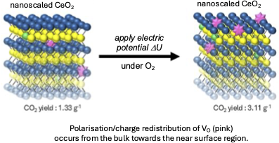
- controlled by the underlying oxidic defect structure. Keywords: cerium oxide; CO oxidation; defect structure; doped cerium oxide; electric potential; Introduction Catalytic CO oxidation is a straightforward approach to reduce CO levels. A variety of catalysts have been synthesized and applied to improve
- particles per unit surface area (N value) were calculated based on three different measurements; these values are summarized in Tables S3–S5 (Supporting Information File 1). According to the values of δ and ε, doping of Gd3+ and La3+ causes a higher defect density in the fcc lattice of nCeO2 as compared to
- (Figure 2 lower panel and Supporting Information File 1, Tables S7–S12 and Figures S26–S29). Without applying potential, trivalent rare-earth doping with La3+ and Gd3+ increases the VO concentration and is expected to increase the population of reduced defect states associated with charge compensation [25


Materials challenges in solid-state sensors for continuous monitoring of ions in water
Beilstein J. Nanotechnol. 2026, 17, 935–973, doi:10.3762/bjnano.17.66
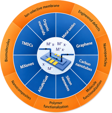
- through strategies such as defect engineering, nanoparticle doping, surface functionalization with organic molecules, or incorporation of advanced recognition elements like metal–organic frameworks, covalent organic frameworks, ion-imprinted polymers, and biomaterials. Hybrid nanocomposites and ion
- noise and hysteresis through clean and defect-controlled interfaces, and must maintain stable electronic properties over time so that any electrical signal change reflects only the analyte concentration, not material instability. Third, the material’s surface must allow for functionalization, enabling
- atoms tend to rearrange, react, or adsorb species to reduce surface free energy, leading to non-ideal, defect-rich surfaces. These defects often cause the film to be n-type doped and form surface states inside the bandgap, affecting charge trapping, catalytic activity, and sensing behavior. Due to their


Enhanced erosion resistance and radiation stability of WC–WO3 nanocomposite films under 100 keV Kr+ ion irradiation
Beilstein J. Nanotechnol. 2026, 17, 922–934, doi:10.3762/bjnano.17.65
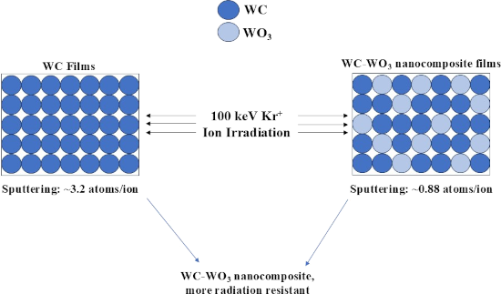
- and oxide phases, as determined from the GIXRD patterns, is summarized in Table 5. Low-energy ion irradiation-induced grain growth has been observed in other nanocrystalline systems [61][68], and a defect-driven mechanism typically explains it. This mechanism posits that the accumulation of
- irradiation-induced point defects, created through collision cascades, leads to mechanical instability in the crystallites. In nanocrystalline materials, collision cascades and subsequent defect formation occur near the grain boundaries. Since grain boundaries act as defect sinks, these defects tend to
- migrate towards them. In such a setting, the cooperative movement of defects towards the grain boundaries stimulates grain boundary migration. This migration results in overall grain growth through atomic jumps of the defects across the grain boundaries [61][68]. The defect density can be estimated via


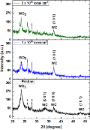

Light-driven ammonia electrooxidation via carbon nitride–ruthenium molecular interfaces
Beilstein J. Nanotechnol. 2026, 17, 854–862, doi:10.3762/bjnano.17.61
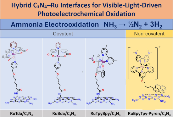
- , Table 1), synthesised in eutectic salt melts, is a highly crystalline ionic variant in which negatively charged nitrogen bridges compensate intercalated metal cations, yielding superior charge carrier mobility, reduced defect density, and extended exciton lifetimes that are of relevance to


Tuning the electronic properties of defect-rich MoS2
Beilstein J. Nanotechnol. 2026, 17, 796–805, doi:10.3762/bjnano.17.56
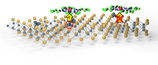
- structural defects significantly affect the electronic properties of the material. The present study utilizes angle-resolved photoelectron spectroscopy (ARPES) and surface-sensitive core-level spectroscopy (SXPS, XAS) with synchrotron radiation to investigate the interfaces between defect-rich MoS2 and
- Fermi energy in such defect-rich MoS2 can be tuned by the subsequent deposition of CoPcF16, which is verified by a shift in Fermi level for the Ne sputtered surface, under complex charge rearrangements including a charge transfer from all the substrates towards the cobalt atom of the organic molecule
- techniques, heterostructuring with (fluorinated) transition metal phthalocyanines (TMPcs) has been shown to modify the interfacial electronic properties of pristine TMDCs [8][9][10]. For the interface between CoPcF16 and defect-free MoS2, a slight doping in the TMDC was recently observed, however without


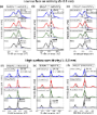
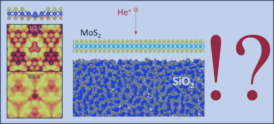
Substrate-dependent pore formation in molybdenum disulfide monolayers under ion irradiation
Beilstein J. Nanotechnol. 2026, 17, 769–780, doi:10.3762/bjnano.17.54
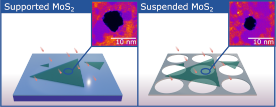
- -)electronic and catalytic functionality [14][15][16][17][18]. Ion irradiation has already proven effective for defect engineering across different energy regimes: Low-energy ions enable implantation with near-atomic precision [19][20][21], kiloelectronvolt ions primarily create point defects in monolayers [22
- ][23][24], and HCIs add potential energy that can lead to larger defect complexes [25]. At megaelectronvolt energies, damage is dominated by electronic excitation and can be tuned by the irradiation geometry (e.g., grazing incidence) [26][27]. While fundamental studies of ion irradiation-induced defect
- and strain-related changes but do not directly resolve the atomic structure [34][35]. This leaves a gap in our understanding of how ion-induced defect formation differs between suspended and substrate-supported 2D materials. We address this gap by directly measuring substrate effects on defect


Recent progress in enhancing built-in electric fields of perovskite solar cells via junction engineering
Beilstein J. Nanotechnol. 2026, 17, 602–621, doi:10.3762/bjnano.17.42
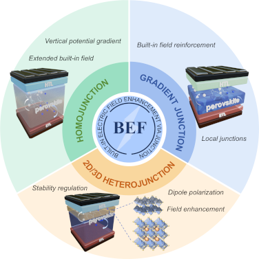
- transport. By contrast, 2D/3D heterojunctions exploit interfacial dipole formation, intrinsic polarization, and phase-penetration effects to amplify and homogenize the BEF, while simultaneously improving energy-level alignment and defect passivation. We systematically compare these strategies within a
- NiOx/NiOx p/p+ homojunction by introducing Ag+ dopants. On the one hand, Ag+ doping increases the hole concentration and coordinates with lattice oxygen, thereby reducing defect states. On the other hand, it shifts the valence-band maximum (VBM) of NiOx from −5.40 eV to −5.46 eV, thereby enhancing band
- defect density. IPA treatment, performed in a glove box at 25 °C with <0.1 ppm H2O, not only formed the n/n+ homojunction but also suppressed iodine vacancy formation and PbI2 accumulation, reducing aging decay from 55% to 19% after 1100 h. In simplified HTL-free device architectures, surface or near



Laser–material interactions in liquids for the synthesis of nanomaterials: current status and perspectives
Beilstein J. Nanotechnol. 2026, 17, 571–575, doi:10.3762/bjnano.17.38
- changes in atomic structure, enabling defect engineering [20]. The broad materials library accessible through LSPC, combined with the wide range of laser, target, and solvent parameters, creates a complex multidimensional optimization space governing nanoparticle size, internal structure, composition, and
- [25][26][27][28], nanoparticle fragmentation intertwined with the generation and collapse of nanobubbles in LFL [29], as well as defect generation during laser-induced melting and resolidification in liquids [30][31]. Experimental investigation of these processes, however, requires characterization
Synthesis of Cu–Mo/TiO2 and Co–Mo/TiO2 photocatalysts for the efficient degradation of organic pollutants in water
Beilstein J. Nanotechnol. 2026, 17, 559–570, doi:10.3762/bjnano.17.37
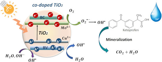
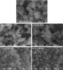
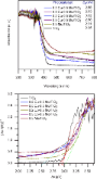
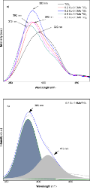
- deconvoluted spectrum of the 0.2 Cu–0.5 Mo/TiO2 material shows a new signal, which could indicate the generation of defects, which are generally related to the ability to capture electrons [36]. The PL intensity increase suggests a poor e−/h+ pair separation. So, it is possible that increased defect-related
- emission may coexist with trapping states. The relationships between PL intensity and photocatalytic activity are very complicated and depend on dopant species [39]. The inhibition of TiO2 phase transformation from anatase to rutile can increase surface oxygen vacancy and defect content [39]. Then, the



Upcycling agroindustrial waste into graphene oxide supports for gold nanoparticles: toward sustainable nanomaterials
Beilstein J. Nanotechnol. 2026, 17, 489–504, doi:10.3762/bjnano.17.32
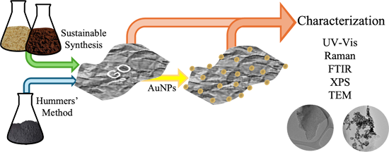
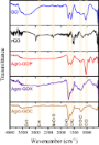
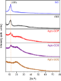
- of functional groups and defect density. Ferrocene was used as a catalytic nucleation agent during pyrolysis as its iron-containing framework facilitates the formation of initial aromatic carbon nuclei and promotes early-stage graphitization at low temperatures [20][21]. All GO samples were also used
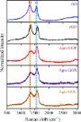
- atoms in aromatic domains and the D band around 1350 cm−1, associated with defects in the crystal lattice such as edges, vacancies, and oxygenated functional groups [38]. The intensity ratio between these peaks (ID/IG) is commonly used as an indicator of structural disorder or defect density in the
- , reducing the number of Raman-active defect sites relative to the G-band signal. Such a scenario is typical for highly oxidized, biomass-derived carbons, where the aromatic domains are broken into very small clusters surrounded by abundant oxygen functionalities [42]. Among the Agro-GO materials, Agro-GOC



Defects and defect-mediated engineering of two-dimensional materials: challenges and open questions
Beilstein J. Nanotechnol. 2026, 17, 454–488, doi:10.3762/bjnano.17.31
- under impacts of energetic particles, such as ions and electrons. At the same time, many concepts of defect production under irradiation in bulk systems are not applicable for 2D materials or require substantial modifications. Various aspects of the physics and chemistry of defects in 2D materials have
- been addressed, and the results of these investigations are presented in hundreds of research papers and review articles. However, the challenges and open questions that still remain in the field have received relatively little attention. These topics were recently addressed at the symposium “Defect
- with low-dimensional targets, and defect-mediated engineering of the properties of 2D systems. We further discuss possible solutions to these problems or suggest “work-arounds”, which should accelerate the progress in the field. Keywords: 2D materials; defects; electron irradiation; ion bombardment





Interconnection morphology effects on the radio frequency response of carbon nanotube sponges
Beilstein J. Nanotechnol. 2026, 17, 343–351, doi:10.3762/bjnano.17.23
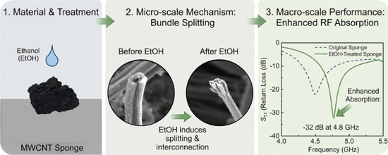
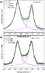
- synthesis of the CNSs was similar. The differences were: (1) No substrate was used. (2) Thiophene (1% v/v) was added to the solution as defect inducer [26][27][28][29] in addition to ferrocene (2.3 wt %), both dispersed in 10 mL of ethanol, stirred for 4 h and injected at a constant rate (5 mL·h−1) into the



Advancing nanolithography: a comprehensive review of materials for local anodic oxidation with AFM
Beilstein J. Nanotechnol. 2026, 17, 275–291, doi:10.3762/bjnano.17.19
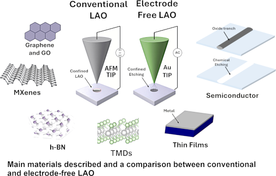
- techniques, such as ALD to create ultrasmooth and defect-free surfaces, further enhance the precision and reproducibility of LAO. 3.2.3 Material-specific approaches. Tailoring LAO parameters to the specific properties of the material being patterned is essential for achieving high-resolution and uniform


Time of flight secondary ion mass spectrometry imaging of contaminant species in chemical vapour deposited graphene on copper
Beilstein J. Nanotechnol. 2026, 17, 200–213, doi:10.3762/bjnano.17.13
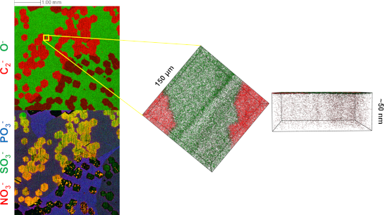
- directly under the graphene after post-growth exposure to atmosphere. This could have implications for better understanding transfer mechanisms that rely on oxidation of the Cu substrate [39][40], defect characterisation [41], or the heat dissipation ability of graphene on Cu [42]. Methods CVD graphene





Reduced graphene oxide paper electrode for lithium-ion cells – towards optimized thermal reduction
Beilstein J. Nanotechnol. 2026, 17, 24–37, doi:10.3762/bjnano.17.3
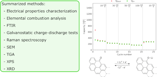
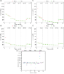
- in defect formation within the graphene structure. However, the G peak intensity behavior after thermal annealing at various temperatures suggests that higher temperatures promote better preservation of areas with sp2-bonded atoms. This peak can also involve a contribution from sp2-hybridized carbon



Microplastic pollution in Himalayan lakes: assessment, risks, and sustainable remediation strategies
Beilstein J. Nanotechnol. 2025, 16, 2144–2167, doi:10.3762/bjnano.16.148
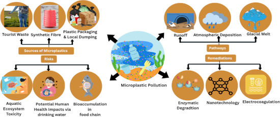
- simultaneously utilizing the abundant UV radiation [75]. It has been demonstrated that the light absorption of ZnO and TiO2 is improved by defect engineering, such as the introduction of oxygen vacancies. According to Kim and Youn, these defects trap light energy, which lowers charge carrier recombination rates


Electron transport through nanoscale multilayer graphene and hexagonal boron nitride junctions
Beilstein J. Nanotechnol. 2025, 16, 2132–2143, doi:10.3762/bjnano.16.147
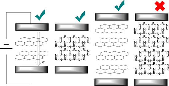
- as a bulk defect. In this work, we deal with periodic graphene models, and we consider only graphitic nitrogen substitutions. The graphitic nitrogen substitution in graphene changes its properties from a zero-bandgap semiconductor to metallic character and decreases its work function [7]. Stone–Wales
- . When the current is calculated for different applied biases, the current/voltage (I/V) curve is obtained. Results and Discussion We start our calculations with a comparison of the electronic properties of graphite, bulk h-BN, graphite with Stone–Wales defect, graphitic nitrogen-doped graphite, and bulk
- h-BN with Stone–Wales defect. For graphite and bulk h-BN, we adopt a graphite unit cell with A–B stacking consisting of two layers and two atoms per layer. We perform geometry optimization, density of states (DOS) calculations, and band structure calculations. For graphite and h-BN with Stone–Wales


Toward clinical translation of carbon nanomaterials in anticancer drug delivery: the need for standardisation
Beilstein J. Nanotechnol. 2025, 16, 2092–2104, doi:10.3762/bjnano.16.144
- peroxidase, or UV-assisted photo-Fenton processes. Notably, oxidised CNOs degrade more readily than their pristine counterparts, due to their higher defect density and greater abundance of oxygen-containing functional groups [42]. These findings highlight that the biodegradability of CNMs strongly depends on




Molecular and mechanical insights into gecko seta adhesion: multiscale simulations combining molecular dynamics and the finite element method
Beilstein J. Nanotechnol. 2025, 16, 2055–2076, doi:10.3762/bjnano.16.141
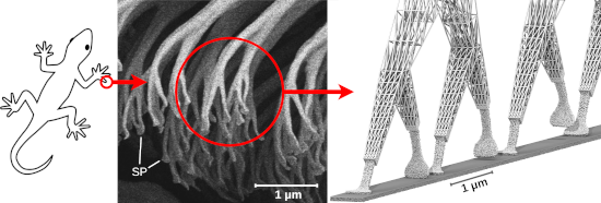
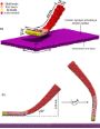
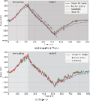
- from 0.5 μm/s to 0.1 m/s [8][9][60], meaning our simulated shear speeds exceeded even the fastest experimental rates several times. This is probably due to a much higher loading rate and a defect-free, smooth substrate in the simulations. The friction coefficient μ is the unitless ratio of frictional






Piezoelectricity of layered double hydroxides: perspectives regarding piezocatalysis and nanogenerators
Beilstein J. Nanotechnol. 2025, 16, 1812–1817, doi:10.3762/bjnano.16.124

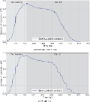
- even surpass, established individual piezocatalysts like BaTiO3 in terms of degradation efficiency or reaction rate, especially when LDHs are ultrathin or doped/composited. However, many BaTiO₃-based systems still offer advantages in stability, availability of well-studied defect engineering, and
- carrier localization effects), or to interfacial electronic interactions that facilitate charge transfer. While these mechanisms may coexist, many publications lack the necessary control experiments (e.g., mechanical stimulation without light/oxidant, photocatalysis without stress, or defect-free samples

Electrical, photocatalytic, and sensory properties of graphene oxide and polyimide implanted with low- and medium-energy silver ions
Beilstein J. Nanotechnol. 2025, 16, 1794–1811, doi:10.3762/bjnano.16.123
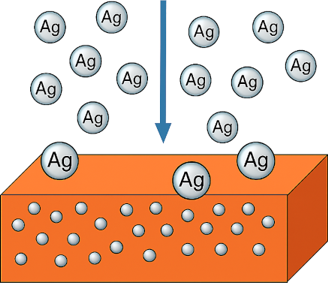
- and enhances both the photocatalytic activity and humidity sensitivity of GO and PI. The most pronounced improvements occurred at higher fluences, where defect generation and partial deoxygenation contributed to optimal performance. Ion implantation thus represents an effective approach for tuning the
- often leads to the displacement of the target nuclei and to significant defect formation in the irradiated material, such as substitution defects [21]. We performed an initial estimation of the ions’ energy losses and range depth of the implanted Ag ions in GO and PI films using SRIM software [22]. This
- collisions dominate the energy loss mechanism. This results in intense atomic displacements near the surface, leading to significant surface damage, defect formation, and localized modifications within a shallow depth (Rp = 25–27 nm). The opposite situation occurs when both GO and PI were implanted with 1.5


Transient electronics for sustainability: Emerging technologies and future directions
Beilstein J. Nanotechnol. 2025, 16, 1545–1556, doi:10.3762/bjnano.16.109
- methods in transient electronics to enhance inorganic encapsulation performance. Yet, it remains difficult to completely eliminate defects within limited film thicknesses. More recently, defect-free layers formed from single-crystalline silicon or its oxide have been explored as waterproof barriers for
- ) Encapsulation strategies use bilayers to block defects, while ALD forms uniform, defect-free films; Mg degradation begins at flaws and spreads in DI water. Figure 2e was adapted from [88], S.-K. Kang et al., “Dissolution behaviors and applications of silicon oxides and nitrides in transient electronics”, Adv


Influence of laser beam profile on morphology and optical properties of silicon nanoparticles formed by laser ablation in liquid
Beilstein J. Nanotechnol. 2025, 16, 1533–1544, doi:10.3762/bjnano.16.108
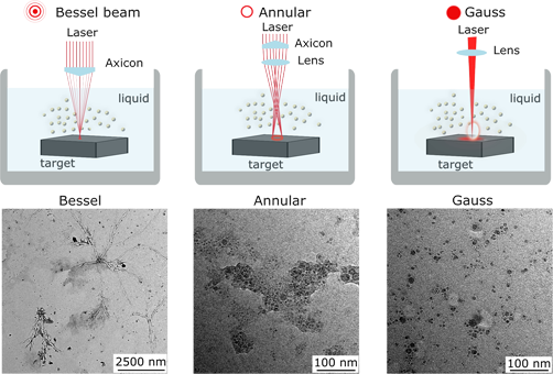
- recombination of free excitons in a quantum confined system [43][44][45], while the blue and green emissions can be attributed to defect states or surface traps generated during the laser ablation process. For example, the observed photoluminescence can originate from the radiative recombination of


Laser processing in liquids: insights into nanocolloid generation and thin film integration for energy, photonic, and sensing applications
Beilstein J. Nanotechnol. 2025, 16, 1428–1498, doi:10.3762/bjnano.16.104
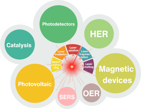
- stability in addition to other benefits like tunable size and morphology, crystalline phases, new compounds and alloys, and defect engineering. These nanocolloids are useful for fabricating different devices mainly with applications in optoelectronics, catalysis, sensors, photodetectors, surface-enhanced
- characteristics, are influenced by the NP size and crystalline quality (Figure 3b,c). LFL also plays a crucial role in tuning the optical properties of NPs. Laser processing affects the defect density and optical bandgap of the particles, as demonstrated by changes in the optical transmission spectra before and
- after LFL treatment. By adjusting processing parameters such as solvent choice, the defect emission, including green defect emissions, can be controlled, providing further opportunities for tailoring the optical properties of NPs for various applications. The mechanisms behind nanoparticle formation