Search results
Search for "film" in Full Text gives 1174 result(s) in Beilstein Journal of Nanotechnology. Showing first 200.
Electrochemical sensing of sildenafil in pharmaceutical formulations using an (S,N)-doped reduced graphene oxide-modified electrode
Beilstein J. Nanotechnol. 2026, 17, 1087–1102, doi:10.3762/bjnano.17.74
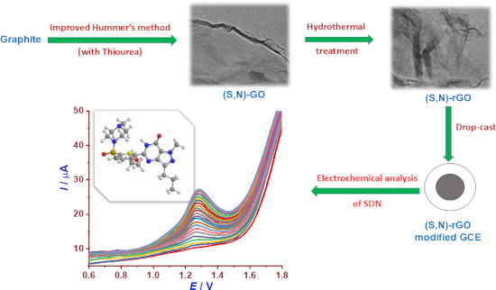
- modified film between independently prepared electrodes. In addition, although the sensor exhibited good selectivity toward the investigated interferents, structurally related electroactive compounds at relatively high concentrations could potentially influence the analytical response. Future work will



Breaking barriers: nanosystems to overcome solubility and permeability challenges of second-generation tyrosine kinase inhibitors
Beilstein J. Nanotechnol. 2026, 17, 1063–1086, doi:10.3762/bjnano.17.73
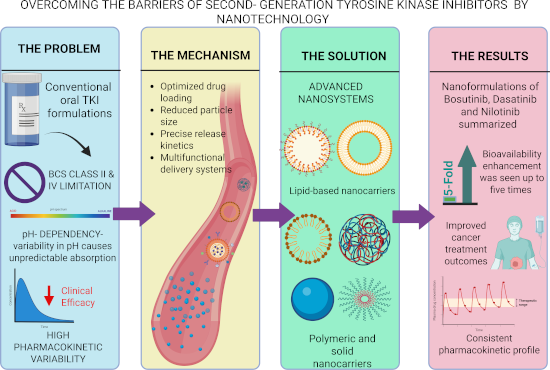
- and Cmax increasing from 200 to 318 ng/mL [70]. Polymeric micelles are composed of amphiphilic polymers that form a hydrophobic core and a hydrophilic shell, enabling efficient encapsulation of lipophilic drugs. DTB-loaded micelles were prepared using a TPGS–Soluplus copolymer via the thin-film
- formed by condensing miR-30a with a cationic copolymer, followed by encapsulation into liposomes using the thin-film hydration technique. The resulting targeted liposomes demonstrated superior inhibition of cell proliferation and migration, along with enhanced cellular uptake, when evaluated in MDA-MB
- microenvironment promoted preferential release at the tumour site. Collectively, these features enhanced the cytotoxic activity of DTB against pancreatic cancer cells [80]. As a potential multifunctional delivery strategy, BTB-loaded high-density lipoprotein (HDL) nanoparticles were formulated using the film


Nanoglasses: a trail towards uncharted regions of vitreous materials and their properties?
Beilstein J. Nanotechnol. 2026, 17, 1047–1062, doi:10.3762/bjnano.17.72
- structure, thermodynamics, and stability of glass–glass interfaces and examine their implications for the design and properties of nanoglasses, highlighting that this approach represents a novel pathway for modifying amorphous materials more broadly. Particular attention is given to columnar thin-film
- , and stability are identified, emphasizing opportunities for integrating nanoglasses into advanced functional thin-film systems. Keywords: columnar thin-film nanoglasses; glass–glass interfaces; mechanical and functional properties; nanoglass; stability; Introduction The advancement of civilization
- deposition, that new structural motifs in previously unexplored regions of the complex energy landscape of glasses may become accessible. One recent example is given by so-called “ultrastable glasses”, where specific conditions for the formation during deposition of thin-film glasses have led to the


Synthesis and characterization of RF-sputtered ZnTe/Cu2−xTe thin films for solar cell applications
Beilstein J. Nanotechnol. 2026, 17, 1016–1027, doi:10.3762/bjnano.17.69
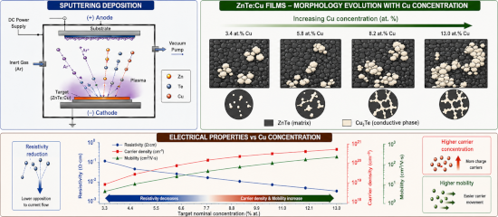
- : back contact materials; Cu2−xTe phases; phase segregation; RF magnetron sputtering; ZnTe thin films; Introduction CdTe solar cells remain one of the leading thin-film photovoltaic technologies due to the near-optimal direct bandgap of CdTe (≈1.45 eV) and its high absorption coefficient (>104 cm−1
- only as a photovoltaic material but also as a contact and buffer layer in thin-film solar cells due to its favorable band alignment with CdTe and its chemical compatibility [9][10][11][12][13][14][15][16]. However, improving its electrical properties without inducing excessive Cu diffusion continues to
- cold pressing at room temperature using a mixture of ZnTe (Aldrich, 99.99%) and CuO (Plasma Science 99.99%) powders. The powder mixtures were homogenized prior to pressing. The targets were prepared with nominal Cu and O concentrations of 0, 3, 8, 10, and 13 atom %. During film growth, the Ar flow in



Development of Protium heptaphyllum essential oil-loaded nanocapsules: experimental design and biological activity
Beilstein J. Nanotechnol. 2026, 17, 974–990, doi:10.3762/bjnano.17.67
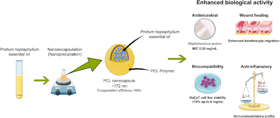
- (30 m length, 0.25 mm and 0.25 µm film thickness) (Agilent Technologies, Inc.). Helium was used as carrier gas at a constant linear velocity of 36.5 cm/s. Samples were injected in splitless mode (split ratio 0:1), with an injection volume of 2 µL of EO diluted in hexane (2 µL in 1 mL). The injector




Materials challenges in solid-state sensors for continuous monitoring of ions in water
Beilstein J. Nanotechnol. 2026, 17, 935–973, doi:10.3762/bjnano.17.66
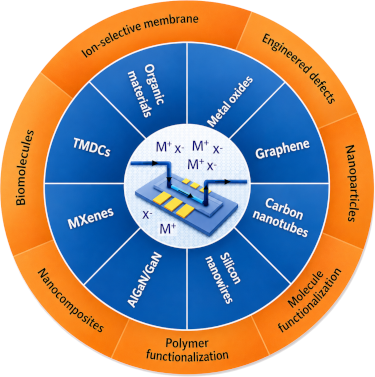
- such as nitrate or phosphate. While they offer fast response times and high sensitivity, electrode fouling and matrix interference can limit their durability in continuous operation. Anodic stripping voltammetry (ASV) sensors build upon this principle, employing thin-film working electrodes (e.g
- film composed of materials such as graphene, reduced graphene oxide, CNTs or conducting polymers (Figure 1j) [11][98][99][100][101][102]. Adsorption or complexation of ions alters the film’s resistance, producing a measurable signal. Selectivity arises from the chemical modification of the sensing
- atoms tend to rearrange, react, or adsorb species to reduce surface free energy, leading to non-ideal, defect-rich surfaces. These defects often cause the film to be n-type doped and form surface states inside the bandgap, affecting charge trapping, catalytic activity, and sensing behavior. Due to their



Enhanced erosion resistance and radiation stability of WC–WO3 nanocomposite films under 100 keV Kr+ ion irradiation
Beilstein J. Nanotechnol. 2026, 17, 922–934, doi:10.3762/bjnano.17.65
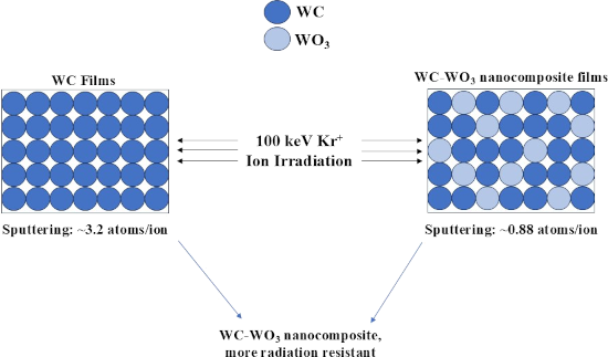
- causes degradation of the PFC material, and the sputtered atoms contaminate the plasma of tokamaks, which is undesirable. The erosion (sputtering) of films is known to be dependent on several factors such as ion energy [55], composition of material and its properties [56][57], film thickness [58], and
- that only the other half of the film is exposed to ion irradiation keeping the covered half pristine, as shown schematically in Figure 1, to determine the sputter yield using Rutherford backscattering spectrometry (RBS) measurements post-irradiation. S1 samples were also irradiated by scanning the
- , , with k being a constant (shape factor; k = 0.9), λ the wavelength of the X-rays, β the full width at half maximum (FWHM) of the peak (in radians), and θ the Bragg angle (in degrees). The calculations showed that the S1 film had a grain size of approximately 17.5 nm, while the S2 film had a grain size



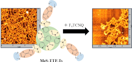
Supramolecular one-dimensional conducting nanofibers from a C3-symmetric tetrathiafulvalene derivative
Beilstein J. Nanotechnol. 2026, 17, 872–881, doi:10.3762/bjnano.17.63
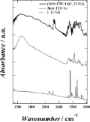
- F4TCNQ. Figure 5 shows the FTIR spectra of neutral F4TCNQ and the (MeS-TTF-Ts)(F4TCNQ)3 charge-transfer complex thin film deposited on a CaF2 substrate. The thin film was prepared by drop-casting a mixed solution of MeS-TTF-Ts in DMSO and F4TCNQ in acetonitrile onto a CaF2 substrate, followed by solvent
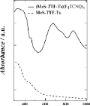
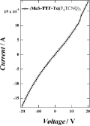
- μm. UV–vis spectra of nanofiber films on quartz substrates formed from MeS-TTF-Ts and the (MeS-TTF-Ts)(F4TCNQ)3 charge-transfer complex. FTIR spectra of neutral F4TCNQ and the (MeS-TTF-Ts)(F4TCNQ)3 charge-transfer complex thin film deposited on a CaF2 substrate. I–V curves of nanofibers composed of


Light-driven ammonia electrooxidation via carbon nitride–ruthenium molecular interfaces
Beilstein J. Nanotechnol. 2026, 17, 854–862, doi:10.3762/bjnano.17.61
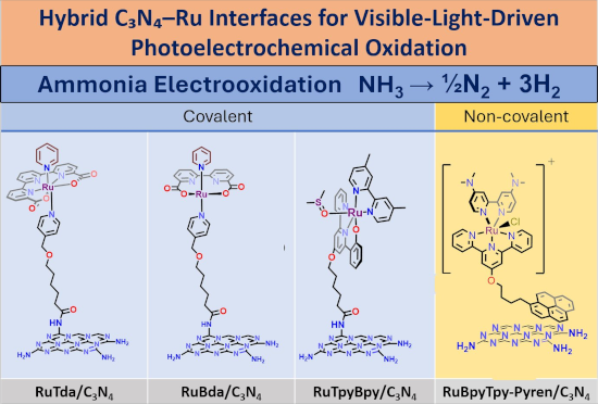
- Jan Holub Pablo Jimenez-Calvo Group of Coordination Chemistry, University of Chemistry and Technology, Prague (UCT, Prague); Department of Inorganic Chemistry, Technická 5, 166 28, Prague, Czech Republic Chemistry of Thin Film Materials, Materials Chemistry Section, Friedrich-Alexander-Universität
- . Heterogeneous catalysts solve the electrode contact problem but introduce their own: In a thick particle film, only the outermost surface layer is electrochemically accessible, while the underlying bulk is not [6][7]. For reactions that require both a light-absorbing semiconductor and a chemically active


Sustainable fabrication of 2D-based devices through reuse of substrates with microfabricated electrodes
Beilstein J. Nanotechnol. 2026, 17, 818–827, doi:10.3762/bjnano.17.58
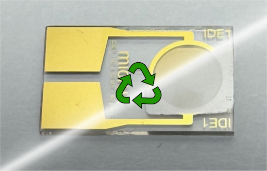
- substrate, making it a more challenging and representative benchmark for cleaning compared to conventional manual exfoliation, which typically results in sparsely distributed flakes that are easier to remove. The MoS2 film was patterned using a vinyl stencil mask, producing a well-defined ‘MoS2’ pattern on
- ) fabrication, initially covered with a large-scale MoS2 film produced by roll-to-roll mechanical exfoliation. Figure 2c,d displays a Ti/Au interdigitated electrode on glass with the 10 µm gap separation, widely used for electrochemistry and biosensing applications [34]. For both cases, the cleaning process
- in uniformly exfoliated large-area flakes adhered to the tape surface. Monolayer MoS2 flakes were obtained by mechanical exfoliation of bulk MoS2 crystals using Nitto SPV 224 tape and subsequently transferring the exfoliated flakes onto Gel-Film (WF 4× 6.0 mil). Candidate monolayer regions were first


Glycerol photoelectrochemical oxidation reaction at carbon nitrides/BiVO4 materials
Beilstein J. Nanotechnol. 2026, 17, 806–817, doi:10.3762/bjnano.17.57
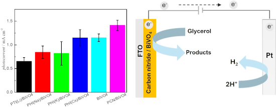
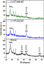
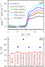
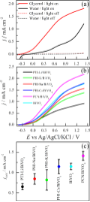
- [29], and bismuth-rich domain within the film [30]. Herein, in order to understand the effect of distinct types of CN materials on CN/BiVO4 heterojunctions, polymeric (PCN), poly(heptazine imide) (PHI) and poly(triazine imide) (PTI) carbon nitrides were synthesized and employed to fabricate CN/BiVO4
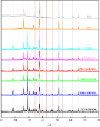
- peaks related to the FTO (since the incident beam interacts with all layers of the material). The main FTO contributions are highlighted by the gray dashed lines. The film containing only BiVO4 presents a diffraction pattern consistent with the monoclinic structure, according to ICDD file 00-044-0081
- characteristic diffraction peaks are observed, whereas for the PCN film on FTO only the characteristic FTO diffraction peaks are detected. FEG-SEM images (Figure 3) were performed on the surface (top view) of the BiVO4 and CN/BiVO4 films. Globular structures characteristic of bismuth vanadate can be recognized




Tuning the electronic properties of defect-rich MoS2
Beilstein J. Nanotechnol. 2026, 17, 796–805, doi:10.3762/bjnano.17.56
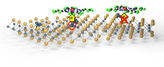
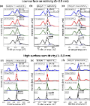
- lower binding energies between the free molecule, indicated by the thicker film (blue line), and the interface (red line) can be mostly attributed to commonly observed screening of the photohole at the interface [9][10][43]. For details on the fitting procedure underlying this conclusion, refer to
- occur at the interface. ARPES band structure of MoS2 before (a–c) and after sputtering (d–f) and the subsequent deposition of a monolayer film of CoPcF16 (g–i), and the integrated valence band structures (j–l) measured at an excitation energy of hυ = 75 eV. Co L2,3 XAS spectra of CoPcF16 coverages in


Substrate-dependent pore formation in molybdenum disulfide monolayers under ion irradiation
Beilstein J. Nanotechnol. 2026, 17, 769–780, doi:10.3762/bjnano.17.54
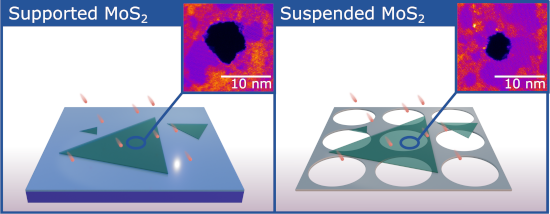
- irradiation of MoS2 on Au, a substrate suitable for mechanical exfoliation is first prepared. A 5 nm Ti adhesion layer is deposited onto SiO2, followed by the deposition of a 25 nm Au film. Immediately after deposition, MoS2 is mechanically exfoliated onto the freshly prepared Au surface. After irradiation on
- layer has dissolved, allowing the PS film with the attached monolayers to be retrieved and cleaned in ultrapure water. The film is then transferred onto a TEM grid and heated for 30 min at 80 °C, followed by 1 h at 130 °C. During this step, slow heating and cooling are essential to avoid damaging the
- TEM grid. Finally, the PS film is dissolved in toluene for 2 h, with the solvent renewed once during the process. After retrieval, the grid is immersed in analytical-grade isopropanol as a final cleaning step and then left to dry. Ion irradiation Irradiation with highly charged xenon ions was done at


Tailoring Ag–Pt nanoalloys through solid-state dewetting: structural and optical insights
Beilstein J. Nanotechnol. 2026, 17, 748–759, doi:10.3762/bjnano.17.52

- nanoscale thickness can be metastable or even intrinsically unstable. This instability leads to the gradual disintegration of the continuous film, and, consequently, the formation of isolated nanoscale islands [13][14][15][16]. This process occurs at temperatures lower than the melting point of the thin
- film. The disintegration mechanism is driven by atomic diffusion, and the tendency of the system is to reduce the surface energy through the formation of isolated islands [17][18][19][20]. This process is governed by the pursuit of balance between the energy needed to create a new surface (surface
- tension) and the energy gained by reducing the total contact area between the film and the substrate (interfacial tension). A comprehensive analysis of the transformation of a thin layer into isolated islands was provided in a series of publications by Thompson and collaborators [13][20][21][22]. They




Cellulose as a photocatalyst support material: extraction, structural features, and environmental applications
Beilstein J. Nanotechnol. 2026, 17, 635–652, doi:10.3762/bjnano.17.44
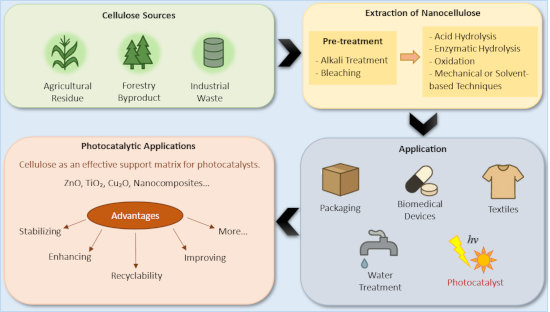
- biosensors using cellulose nanocrystals combined with magnetite to create (x-CNC)-Fe3O4 systems, which demonstrate excellent biocompatibility and are tailored for glucose detection. These biosensors are often fabricated as thin-film strips that can be applied directly onto the skin or tongue, where they
- inorganic phases such as TiO2 on its fibrous surface, allowing researchers to exploit its natural abundance and structural characteristics to develop sustainable photocatalytic composites [101]. Mohamad Azuwa Mohamed et al. prepared a regenerated cellulose (RC) thin film using recycled newspaper as the
- cellulose source, creating a sustainable and low-cost material designed for photocatalytic thin film applications. To evaluate its performance, they tested the photocatalytic activity of the RC/N-TiO2 composite by examining its ability to degrade methylene blue under both artificial UV and visible light


Two-step laser synthesis of Ag@TiO2 nanomaterials for the photocatalytic degradation of rhodamine B
Beilstein J. Nanotechnol. 2026, 17, 622–634, doi:10.3762/bjnano.17.43
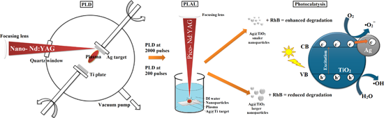
- were deposited onto titanium substrates (purity > 99.9%, ThermoScientific) using nanosecond pulsed laser deposition in a vacuum. A 1 mm thick Ag plate (purity > 99.99%, GoodFellow) served as the laser target, with both the Ti substrate and Ag target rotating to ensure uniform film formation. An Nd:YAG
- laser (1064 nm, 300 mJ, 5 Hz, 5 ns) was focused onto the Ag target with a fluence of 12 J·cm−2. Different silver film thicknesses were obtained by varying the number of laser pulses (200 and 2000). Subsequently, the Ag-coated Ti plates and a pure Ti substrate underwent picosecond pulsed laser ablation


Recent progress in enhancing built-in electric fields of perovskite solar cells via junction engineering
Beilstein J. Nanotechnol. 2026, 17, 602–621, doi:10.3762/bjnano.17.42
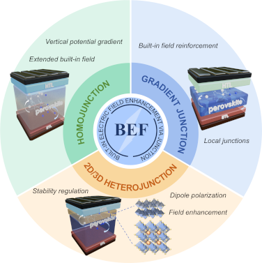
- controlled doping and orientation modulation, thereby suppressing nonradiative recombination and improving carrier extraction. Gradient junctions introduce continuous compositional or bandgap tilts across the film thickness, enabling depth-extended electric fields and improved spatial continuity of charge
- advantages include a continuous potential distribution, fewer additional interfaces, and good compatibility with existing fabrication processes. In contrast, gradient junctions employ gradual variations in composition, ion concentration, dimensionality, or bandgap along the film thickness to create a
- continuous barrier-reducing channel across the film [15], a strategy that emphasizes longitudinal potential continuity and a “capacitive accumulation” effect, which maintains an effective driving force over a larger thickness and is often accompanied by improved crystallinity and stress release




Probing tribological evolution in atomically thin MoS2 at different scales
Beilstein J. Nanotechnol. 2026, 17, 586–597, doi:10.3762/bjnano.17.40
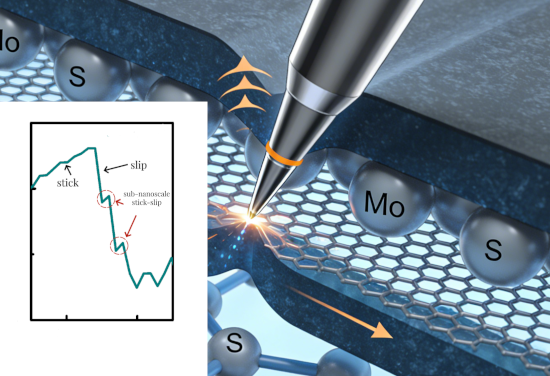
- film and reduces its out-of-plane deformability. Although more interlayer spacing regions exist in thicker films, the enhanced interlayer coupling restricts the independent deformation of each layer, leading to an overall reduction in the ability of the film to conform to the AFM tip and adjust to the
- strengthening effect discussed earlier. For the 4L MoS2 film, the bottom layer is strongly adsorbed on the SiO2/Si substrate via van der Waals interaction, while the upper three layers are less strongly bound to each other. During AFM sliding, the tip drags the top layer, and the weak interlayer van der Waals


Impacts of annealing on structural and photophysical properties of zinc phthalocyanine adsorbed on graphene
Beilstein J. Nanotechnol. 2026, 17, 576–585, doi:10.3762/bjnano.17.39
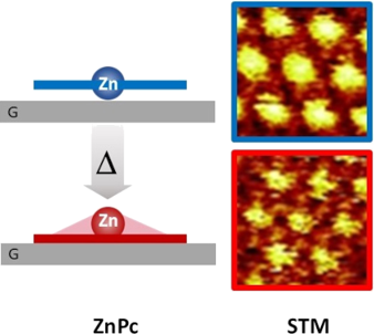
- a large background covering the 600–2500 cm−1 region (i.e., 660–750 nm in terms of emitted wavelength) with a quantum yield less than 10−6 as roughly estimated by comparison with the typical signal obtained from a reference standard composed of a rhodamine 6G doped PMMA thin film. This fluorescent


Probing internal continua and atomic ultrafast charge transfer within size-controlled nanoparticles by post-collision interaction in core-hole clock spectroscopy
Beilstein J. Nanotechnol. 2026, 17, 505–514, doi:10.3762/bjnano.17.33
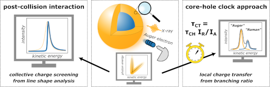
- % of the Auger signal originates solely from the shell, while, in the shell with eleven double layers, this value increases to over 60% [32]. Given that the QDs are covered with a surface layer of long-chain hydrocarbon ligands (hexadecylamine) and that such films can reach film thicknesses of 1–2 nm



Defects and defect-mediated engineering of two-dimensional materials: challenges and open questions
Beilstein J. Nanotechnol. 2026, 17, 454–488, doi:10.3762/bjnano.17.31
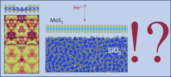
- difficult to obtain. Similarly, in thin film growth involving volatile components (e.g., chalcogens), the composition of the film is determined by the compound with the lowest formation enthalpy and not by the atom flux. For example, during molecular beam epitaxy (MBE) growth of chalcogenides, chalcogen
- atoms are generally supplied in excess, and the film will adopt the lowest-energy composition. In these cases, the stoichiometry of the film is not determined by the composition of the source materials but by the thermodynamic stability of the film. So again, in thin film growth, obtaining compositions





Nanocarrier-integrated multilayer films produced by 3D printing for improved skin adhesion and curcumin photostability
Beilstein J. Nanotechnol. 2026, 17, 440–453, doi:10.3762/bjnano.17.30
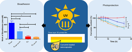
- content and the non-encapsulated curcumin content. Production of the printing Inks Three different polymeric hydrogels or hydrogel blends were produced, corresponding to the three distinct layers of the film. Table 1 presents the composition of the different hydrogels prepared and used as printing inks
- for the present study. Some hydrogels were prepared solely for comparative purposes and were used during the characterisation step. Chitosan was the polymer used to produce the hydrogel for the bottom layer of the film. This natural polymer was initially mixed with glycerine in a porcelain mortar, and
- nanocapsules (FC-NC) or curcumin solubilised in a hydroalcoholic solution (FC) were 3D-printed by semi-solid extrusion using a BioEdTech printer (São Paulo, Brazil) and three different hydrogels as printing inks. HG-Chi was used as the printing ink to produce the bottom layer of the film. Subsequently, two


Polycatecholamine nanocoatings on stainless steel: the effect on attachment of human fibroblasts and platelets
Beilstein J. Nanotechnol. 2026, 17, 365–380, doi:10.3762/bjnano.17.25
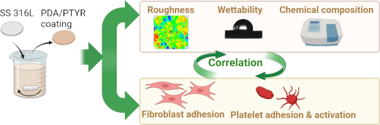
- longest time of coating. Images taken directly after coating (Figure 5a,b,e,f) show the initial coating morphology. The surface of SS-PDA 10 min could not be clearly distinguished with SEM; however, the surface of SS-PDA 4 h presented a full coverage with a polymer film. After 28 d of constant washing




Interconnection morphology effects on the radio frequency response of carbon nanotube sponges
Beilstein J. Nanotechnol. 2026, 17, 343–351, doi:10.3762/bjnano.17.23
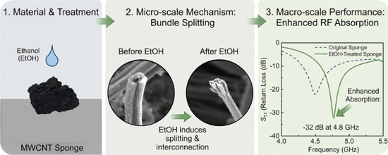
- , Italy 10.3762/bjnano.17.23 Abstract In this work, the high-frequency response of a multiwalled carbon nanotube (MWCNT) film grown on a silicon substrate is compared with that of MWCNT sponges (CNSs). Different from the CNT film, CNSs are a self-standing material that can operate in the absence of a
- , also an actual performance gain. The antenna built from CNSs shows an enhanced response gain compared with that of the MWCNT film, with both antennas having a maximum positioned around 4.8 GHz. After identifying the best CNT-based sample, the experiment focused on improving the CNS antenna’s response
- applied for these tests, and an increase in the response up to 45% was found for the two studied positions. Keywords: carbon nanotube film; carbon nanotube sponge; chemical vapour deposition; monopole RF antenna; Introduction Most radio frequency (RF) applications rely on the use of conductors with low




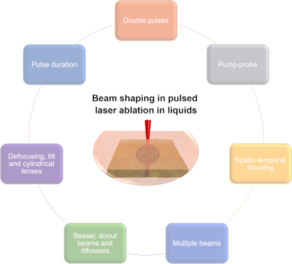
Beam shaping techniques for pulsed laser ablation in liquids: Unlocking tunable control of nanoparticle synthesis in liquids
Beilstein J. Nanotechnol. 2026, 17, 309–342, doi:10.3762/bjnano.17.22