


Search results
Search for "exciton" in Full Text gives 106 result(s) in Beilstein Journal of Nanotechnology.
Light–matter interactions in two-dimensional layered WSe2 for gauging evolution of phonon dynamics
Beilstein J. Nanotechnol. 2020, 11, 782–797, doi:10.3762/bjnano.11.63
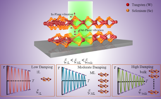
- 1.90× that of the out-of-plane vibrational mode over T = 79 K up to 523 K. To provide energy from external stimuli, as T and P were increased, peak broadening in the PL spectra of the A-exciton was observed. From this, a phonon concentration was tabulated using the Urbach formulism, which increased
- work reported τ over a range T = 4.4–300 K in naturally abundant and isotopically pure WSe2 grown by the chemical vapor deposition (CVD) method [29]. In one of our recent works, exciton dynamics and phonon lifetimes in CVD-grown and mechanically exfoliated 1L WSe2 nanosheets were analyzed and τ
- , obtained from temperature-dependent Raman measurements in the mode, was found to decrease at high temperature due to increased phonon-induced scattering events which eventually also reduces the exciton density in WSe2 [30]. In this present work, we studied the phonon lifetime, τ, and phonon concentration
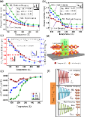
Soybean-derived blue photoluminescent carbon dots
Beilstein J. Nanotechnol. 2020, 11, 606–619, doi:10.3762/bjnano.11.48
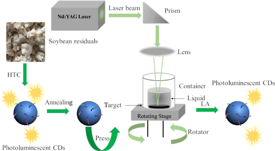
- irreversible change in the energy gap induced by the annealing. It is known that the temperature dependence of the energy gap for the fluoresence of CDs can be expressed as [42] where Eg(T) is the energy gap at temperature T, S is the Huang–Rhys factor representing the coupling strength between exciton and


Implementation of data-cube pump–probe KPFM on organic solar cells
Beilstein J. Nanotechnol. 2020, 11, 323–337, doi:10.3762/bjnano.11.24
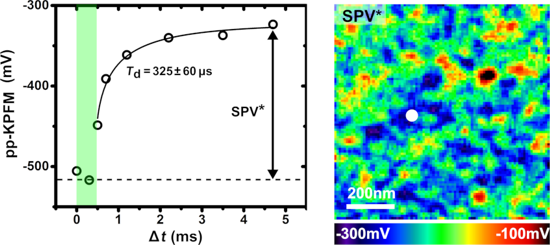
- global electrostatic landscape probed by KPFM in the dark state [20]. The photocharging dynamics can be understood as follows. After exciton splitting and dissociation of the charge transfer states at the D–A interfaces, the photogenerated carriers experience a drift-diffusion limited by the carrier
- the 10 nm scale, to maximize the donor–acceptor interfacial area where the excitons are dissociated and to overcome the short-exciton diffusion length. The vast majority of solution-processed D–A blends actually display more complex morphologies. For instance, they can feature a three-component
- electron–hole annihilation at the D–A interfaces. Here, we do not discuss the losses by exciton relaxation or by pairwise recombination of the CT state. The free carriers can also be trapped in tail states [25] before recombining with free unpaired counter charges. This slower recombination process is




Molecular architectonics of DNA for functional nanoarchitectures
Beilstein J. Nanotechnol. 2020, 11, 124–140, doi:10.3762/bjnano.11.11
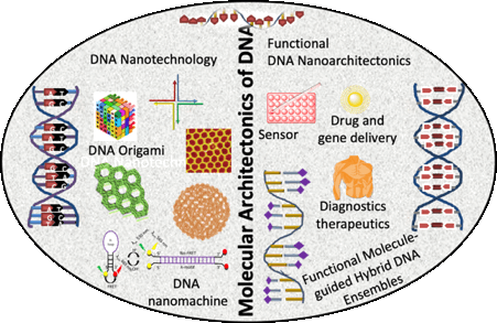
- double-helical DNA through ᴅ- and ʟ-threolinol linkers to analyze the molecular exciton theory of heterodimeric chromophores [95]. NMR studies revealed the antiparallel orientation of the two dyes across the duplex strand. Further studies indicated that the increment in dye number could dramatically


Recent progress in perovskite solar cells: the perovskite layer
Beilstein J. Nanotechnol. 2020, 11, 51–60, doi:10.3762/bjnano.11.5

- perovskites is lower than that of their 3D counterparts because of the lower carrier mobility, the wide optical bandgap, the low conductivity and the large exciton binding energy. Therefore, Priya et al. [8] created a methylammonium (MA)-based 2D perovskite film by using the vapor-fumigation technique. The
- resulting films benefit from a higher conductivity, better carrier transport properties and a smaller exciton binding energy compared to traditional 2DRP perovskites based on bulky BA. Ultrastable 2DRP PSCs with a certified PCE of 16.6% were obtained. Their initially determined properties were degraded by


Formation of metal/semiconductor Cu–Si composite nanostructures
Beilstein J. Nanotechnol. 2019, 10, 2497–2504, doi:10.3762/bjnano.10.240
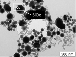
- [10], or can even consist of three layers [11][12]. These variations can be useful for practical applications, e.g., for enhancing the absorption capacity of particles or for plasmon–exciton interaction [13]. The presence of an inorganic shell on a metal particle often leads to a significant


Nontoxic pyrite iron sulfide nanocrystals as second electron acceptor in PTB7:PC71BM-based organic photovoltaic cells
Beilstein J. Nanotechnol. 2019, 10, 2238–2250, doi:10.3762/bjnano.10.216
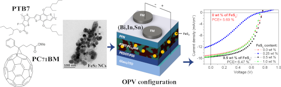
- characteristics could facilitate exciton dissociation, charge transport and collection processes, and thus increase the overall PCE value. Figure 5a shows the UV–vis absorption spectra of the OPV active layer at different concentrations of FeS2 as well as that of the pure FeS2 film. The spectrum of the PTB7
- correlation with the absorption of the PTB7:PC71BM blend. The EQE of devices with 0.5 wt % of FeS2 is higher than that of the reference OPV cells, which could be attributed to a better charge separation (exciton dissociation enhancement) as well as enhanced carrier transport and collection in the
- corresponding devices [21][28][43][50]. In other words, a reduction of the exciton recombination can take place while additional electron charge pathways are established in the active layer. Furthermore, a better charge balance (free holes/electrons) develops, and thus, the overall OPV performance is improved


First principles modeling of pure black phosphorus devices under pressure
Beilstein J. Nanotechnol. 2019, 10, 1943–1951, doi:10.3762/bjnano.10.190
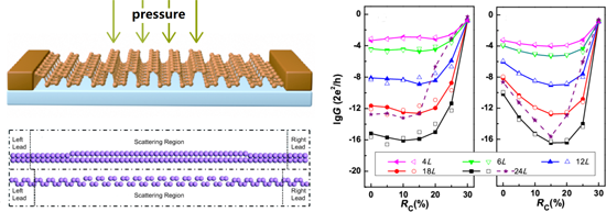
- funnel effect in monolayer BP [13], which describes the possibility of controlling exciton motion by means of inhomogeneous strains. They found that the funnel effect in BP is much stronger than that in MoS2, and more important, shows opposite behavior to that in MoS2. Excitons in BP are mainly




Photoactive nanoarchitectures based on clays incorporating TiO2 and ZnO nanoparticles
Beilstein J. Nanotechnol. 2019, 10, 1140–1156, doi:10.3762/bjnano.10.114
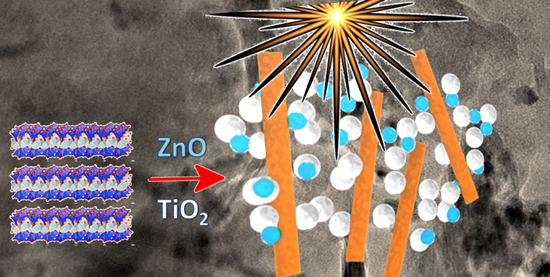
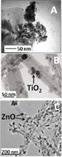
- metal oxides exhibit a large exciton binding energy, large piezoelectric constants and strong photoluminescence. This is of interest not only for applications as photocatalysts but also as sensors, solar cell devices, disinfectants, and cosmetics [137][138]. As discussed above, the dispersion of the



CuInSe2 quantum dots grown by molecular beam epitaxy on amorphous SiO2 surfaces
Beilstein J. Nanotechnol. 2019, 10, 1103–1111, doi:10.3762/bjnano.10.110
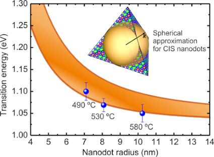
- this family of materials [5], new solar-cell architectures based on nanostructures have been proposed [6][7][8][9]. Examples of such architectures are intermediate-band solar cells [10], solar cells based on multi-exciton generation [11][12], quantum dot solar cells [13][14][15], and others [16], all
- radiative recombination of free excitons (FE) and of bound excitons (B), as well as the no-phonon line of the bound exciton (BNP) as confirmed from PL measurements performed under the same experimental conditions of a Si substrate. After the deposition of a CdS layer on top of the three as-grown nanodot
- in more detail, simple quantum confinement calculations were carried out considering a hard wall spherical QD of radius R and the wetting layer as a hard wall quantum well (QW) of thickness L. The calculations consider the free exciton emission for the QD and QW, respectively. The first transition


Correlation of surface-enhanced Raman scattering (SERS) with the surface density of gold nanoparticles: evaluation of the critical number of SERS tags for a detectable signal
Beilstein J. Nanotechnol. 2019, 10, 1016–1023, doi:10.3762/bjnano.10.102
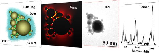
- plate placed at the bottom of a cell containing a 10−4 M NaCl solution in double distilled water [18][19][41]. Dye solutions of either hexacyanin 3 (HITC, perchlorate, Exciton), malachite green (MG, oxalate salt, Sigma-Aldrich) or malachite green isothiocyanate (MGITC, Invitrogen) were added to a 2 nM


Oriented zinc oxide nanorods: A novel saturable absorber for lasers in the near-infrared
Beilstein J. Nanotechnol. 2018, 9, 2730–2740, doi:10.3762/bjnano.9.255
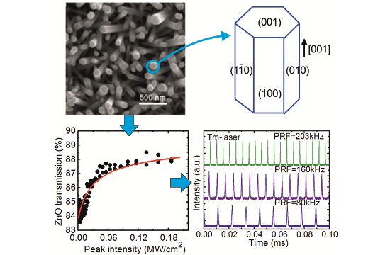
- exciton binding energy (60 meV) [3], allowing for efficient excitonic photoluminescence at room temperature, and due to their good mechanical and thermal stability. Arrays of ZnO NRs can be grown on various substrates (e.g., Si, Al2O3, glass) either by gas phase processes (e.g., by vapor–liquid–solid



Two-dimensional semiconductors pave the way towards dopant-based quantum computing
Beilstein J. Nanotechnol. 2018, 9, 2668–2673, doi:10.3762/bjnano.9.249
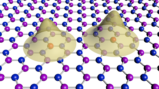
- the effect of a non-local dielectric function can be reproduced by a dielectric constant given by its average within the radius of the wave-function [36], dramatically simplifying the energy calculations. In [36], this simplification has been proven to be accurate for the calculation of the exciton


![[Graphic 7]](/bjnano/content/inline/2190-4286-9-249-i7.svg?max-width=637&scale=1.18182) and energy for one electron bound to a donor pair
and energy for one electron bound to a donor pair ![[Graphic 8]](/bjnano/content/inline/2190-4286-9-249-i8.svg?max-width=637&scale=1.18182) as a function of R. For R = 2a*, ...
as a function of R. For R = 2a*, ...

Polarization-dependent strong coupling between silver nanorods and photochromic molecules
Beilstein J. Nanotechnol. 2018, 9, 2657–2664, doi:10.3762/bjnano.9.247
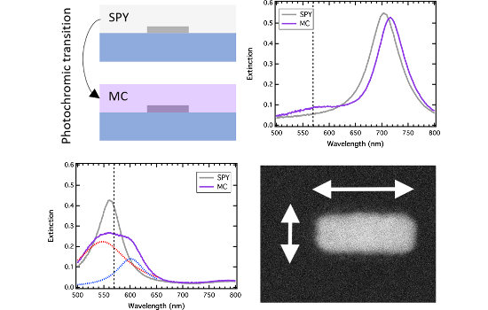
- macroscopic optical components, such as lenses [12] or sunglasses [13]. From the plasmonic perspective, the photochromic molecules can allow for the active control of the plasmonic resonance. The coupling between molecular exciton and plasmonic resonance can lead to weak [14] or strong coupling [15]. The
- latter is always observed when the plasmon or the molecular exciton presents a large oscillator strength and leads to the splitting of the main resonance. We previously demonstrated a reversible, strong coupling between silver cylindrical nanoparticles and photochromic molecules, both considered as
- resonators, they used lattice resonances and benefited from the sharp Fano-type resonance to observe the strong coupling anti-crossing behavior [22]. In our case, each resonator (the LSPR and the molecular exciton) presents a large full width at half maximum (FWHM). Indeed, the black curve of the Figure 2b



Lead-free hybrid perovskites for photovoltaics
Beilstein J. Nanotechnol. 2018, 9, 2209–2235, doi:10.3762/bjnano.9.207
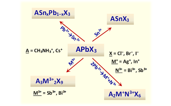
- luminescent Cs3Bi2X9 NCs [159]. A study of single-crystal and polycrystalline MABI showed that both materials have a long exciton lifetime and a high carrier mobility [161][163]. A transient absorption study of MABI crystals showed only a minor change of the exciton dynamics when the crystal size was reduced


Numerical analysis of single-point spectroscopy curves used in photo-carrier dynamics measurements by Kelvin probe force microscopy under frequency-modulated excitation
Beilstein J. Nanotechnol. 2018, 9, 1834–1843, doi:10.3762/bjnano.9.175
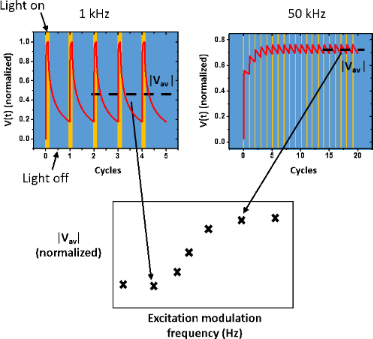
- account the built-up time of the SPV, which is the time needed for the surface photovoltage to appear in the first place. This time is associated with the exciton generation, charge dissociation and charge transport along the material so that a photo-generated surface potential can be detected using KPFM
- the effective time needed for exciton generation, dissociation and carrier separation. On the other hand, in the case of some organic photovoltaic (OPV) samples, the SPV built-up time can be attributed to the effective time needed to fill lower energy states (traps). In a more general way, it can be


Photoluminescence of CdSe/ZnS quantum dots in nematic liquid crystals in electric fields
Beilstein J. Nanotechnol. 2018, 9, 1544–1549, doi:10.3762/bjnano.9.145
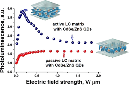
- dependence on two independent, but spectrally overlapping, processes. The first process involves the recombination of the so-called “internal” exciton with energy close to the width of the band gap and a decay time of about 20–30 ns, depending on the size of the quantum dots. The second process is associated
- with recombination of the so-called “charged” exciton, which appears in a charged nanoparticle for a period of time until one of the photoexcited electrons is trapped. The average decay time of a “charged” exciton is about 1–3 ns [24][25]. The increase in the relative decay time of the QDs luminescence


Absence of free carriers in silicon nanocrystals grown from phosphorus- and boron-doped silicon-rich oxide and oxynitride
Beilstein J. Nanotechnol. 2018, 9, 1501–1511, doi:10.3762/bjnano.9.141
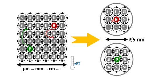
- Si, typical dopant ionization energies are in the range of ≈50 meV. If the size of the Si crystal approaches the exciton Bohr-radius, strong quantum confinement sets in and the valence- and conduction band ground state energies shift to lower and higher energies, respectively. As a consequence, the
- used, which correspond to the excitation regime with normal Auger recombination of excitons, excluding bimolecular recombination [46]. If an additional free carrier (electron from P-donor or hole from B-acceptor) would be present in a Si NC, the generated exciton(s) could efficiently and quickly


Computational exploration of two-dimensional silicon diarsenide and germanium arsenide for photovoltaic applications
Beilstein J. Nanotechnol. 2018, 9, 1247–1253, doi:10.3762/bjnano.9.116
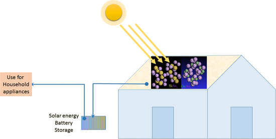
- suitable for photovoltaic applications, such as excellent visible light absorption, favorable exciton formation, and charge separation are equally essential for two-dimensional (2D) materials. Here, we systematically study 2D group IV–V compounds such as SiAs2 and GeAs2 with regard to their structural
- dynamic stability of the compounds, which is inferred by analyzing their vibrational normal mode. SiAs2 and GeAs2 monolayers possess a bandgap of 1.91 and 1.64 eV, respectively, which is excellent for sunlight harvesting, while the exciton binding energy is found to be 0.25 and 0.14 eV, respectively
- exciton binding energy was obtained [32]. Results and Discussion The crystal structures of SiAs2 and GeAs2 are orthorhombic with the space group Pbam (no. 55) having eight symmetry operators or atoms in the unit cell [4]. Figure 1 shows the side views of the bulk configurations of SiAs2 and GeAs2 with


Electro-optical interfacial effects on a graphene/π-conjugated organic semiconductor hybrid system
Beilstein J. Nanotechnol. 2018, 9, 963–974, doi:10.3762/bjnano.9.90
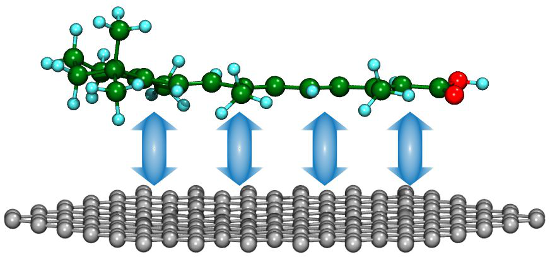
- multilayered RA sample portrays a substantial increase in PL intensity as the temperature decreases. These features are understood in light of previous studies, which demonstrated that the exciton mobility in organic semiconductor occurs via both dipole–dipole coupling (Förster transfer) and thermally assisted
- migration [28]. At low temperatures, the volume probed by an exciton is reduced, which reduces the interaction probability with nonradiative traps or defects, reflecting an increase in the emission efficiency of the organic compound [29]. Moreover, the increase in emission efficiency with decreasing
- interface-induced highly ordered SAM structure leads to a reduction in nonradiative quenching pathways, resulting in a temperature-independent high efficiency optical emission state. Even though the exciton thermal energy is smaller at low temperatures and nonradiative processes would be suppressed, the




Valley-selective directional emission from a transition-metal dichalcogenide monolayer mediated by a plasmonic nanoantenna
Beilstein J. Nanotechnol. 2018, 9, 780–788, doi:10.3762/bjnano.9.71
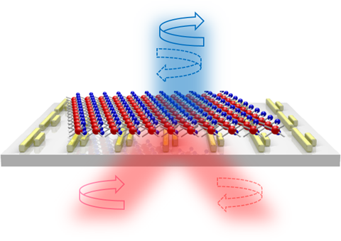
- be reversed if the emitter is placed on the opposite side of the antenna. As such, the currently proposed schemes can not be employed to control the emission of delocalized chiral emitters, such as emission from exciton from the two valleys of a 2D TMDC material. Here, we propose a plasmonic TMDC
- arrow) to the other (dashed arrow). Design and implementation Since the emission from the TMDC monolayer solely comes from the in-plane exciton or trion charge carriers [44], the TMDC emitters could be practically modeled as chiral point-dipole emitters placed in the vicinity of the photonic structure


Surface-plasmon-enhanced ultraviolet emission of Au-decorated ZnO structures for gas sensing and photocatalytic devices
Beilstein J. Nanotechnol. 2018, 9, 771–779, doi:10.3762/bjnano.9.70
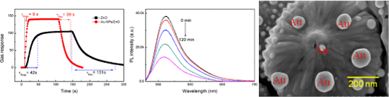
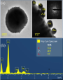
- revealed that ZnO sub-micrometer spheres were deposited on the glass substrates and Au-decorated ZnO nanostructures were confirmed. Using photoluminescence (PL) spectra and time-resolved photoluminescence (TRPL) measurements, we investigate the SPR characteristics and ZnO exciton peaks, which complement
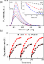
- , was equal to 150 ps and 995 ps for Au NP/ZnO samples, respectively. This is comparable to the values for ZnO found to be 197 ps and 1.05 ns, respectively. This may imply that the charge transfer occurring between the Au NPs and ZnO is responsible for the faster decay time components due to exciton




Temperature-tunable lasing from dye-doped chiral microdroplets encapsulated in a thin polymeric film
Beilstein J. Nanotechnol. 2018, 9, 379–383, doi:10.3762/bjnano.9.37
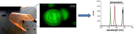
- Exciton. It is added to the chiral mixture with a concentration of 0.3 wt %. Figure 2 shows the fluorescence spectrum of the DCM dye. First, the dye-doped CLC mixture is used to prepare the emulsion. With respect to [17], the emulsion is prepared with the same procedure, but it contains only one type of


Dopant-stimulated growth of GaN nanotube-like nanostructures on Si(111) by molecular beam epitaxy
Beilstein J. Nanotechnol. 2018, 9, 146–154, doi:10.3762/bjnano.9.17
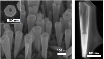
- as well as two PL lines corresponding to D0XA and D0XB excitons bound to neutral donors [36]. In our study we did not expect acceptor–bound excitons since the studied nanostructures were Si-doped. Figure 3 shows that four exciton lines of the PL spectra of our samples can be distinguished, namely: XA
- , XB, D0XA and D0XB. As one can see, in our spectra, phonon replicas of exciton transitions related to a longitudinal optical phonon with 93 meV energy [37] (XA – 1 LO, D0XA – 1 LO and D0XB – 1 LO) are observed. Features in the region of 3.43 eV indicate transitions related to structural defects [38
- much stronger in doped NWs from samples 3 and 4 (red and blue curves, correspondingly), however the free exciton PL band XA is also present. The difference in the ratios of D0XA to D0XB peak intensities for samples 3 and 4, which were synthesized under very similar growth conditions (difference in the


Optical contrast and refractive index of natural van der Waals heterostructure nanosheets of franckeite
Beilstein J. Nanotechnol. 2017, 8, 2357–2362, doi:10.3762/bjnano.8.235
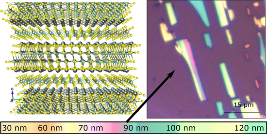
- generation of excitons [27]. In the case of franckeite we do not see any sharp resonance that could be attributed to exciton-generation processes within the explored range, as expected because the absorption band edge is far from the measurement window. Note that, to our knowledge, this information was not





