Search results
Search for "semiconductor" in Full Text gives 647 result(s) in Beilstein Journal of Nanotechnology. Showing first 200.
Ion-induced surface reactions and deposition from Pt(CO)2Cl2 and Pt(CO)2Br2
Beilstein J. Nanotechnol. 2024, 15, 1427–1439, doi:10.3762/bjnano.15.115

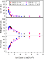
- , deposition strategies in various applications, such as circuit editing and lithographic mask repair in the semiconductor industry [7][8][9][10][11][12] as well as the growth of functional materials for magnetism [13][14][15][16], superconductivity [17], and sensing [18][19]. Compared to FEBID, FIBID operates



Lithium niobate on insulator: an emerging nanophotonic crystal for optimized light control
Beilstein J. Nanotechnol. 2024, 15, 1415–1426, doi:10.3762/bjnano.15.114
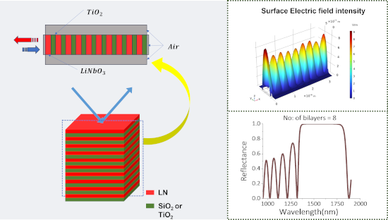
- challenging due to its ultrafast nature. In 2022, Quach et al. presented an innovative model of a quantum battery [37]. This device comprises a DBR structure-based microcavity that encloses an organic semiconductor molecular dye, named Lumogen-Forange (LFO). The DBRs comprised 10 bilayers of SiO2/Nb2O5 in the
- and driving coherent interactions with the organic semiconductor molecules. Secondly, enabling the measurement of the evolution of stored energy and the differential reflectivity induced by the pump pulse, which is essential for monitoring the charging dynamics at a femtosecond resolution. The


Various CVD-grown ZnO nanostructures for nanodevices and interdisciplinary applications
Beilstein J. Nanotechnol. 2024, 15, 1390–1399, doi:10.3762/bjnano.15.112
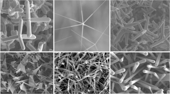
- electronic/optoelectronic devices, energy storage/generation systems, and renewable energy conversion devices with high performance and low-power consumption [1][2][3]. In comparison to semiconductors, ZnO has attracted much more attention. This is due to ZnO having outstanding semiconductor behaviours in
- microcavities [9]. Additionally, it is a transparent semiconductor with significant piezoelectricity [10]. These noble characteristics suggest ZnO to be a potential material in the fabrication of UV/blue/green LEDs, solid-state random lasers, UV-absorption devices, and nanogenerators [9][11][12][13]. Magnetic



Green synthesis of carbon dot structures from Rheum Ribes and Schottky diode fabrication
Beilstein J. Nanotechnol. 2024, 15, 1369–1375, doi:10.3762/bjnano.15.110
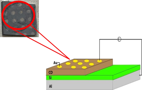
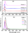
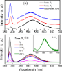
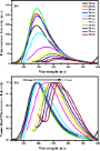
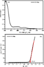
- were calculated as 566 nm and 5.25 eV, respectively. The ideality factor and the measured barrier height (Φb) of the CDs-based Schottky diode were calculated as 9.1 and 0.364 eV, respectively. The CDs were used as semiconductor material in a Schottky diode, and the diode exhibited rectification
- electrical current. There are many types of diodes, such as Zener diodes, crystal diodes, and Schottky diodes, and each type has different features and is used for different purposes. Schottky diodes contain a metal–semiconductor junction. This structure differs from other diodes because of its high
- of demonstrating the applicability of CDs in the field of electronics, apart from sensor studies, which are common application areas, and in terms of introducing new semiconductor materials to the field of electronics. Experimental Materials Rheum ribes was purchased from the market, washed, and




Out-of-plane polarization induces a picosecond photoresponse in rhombohedral stacked bilayer WSe2
Beilstein J. Nanotechnol. 2024, 15, 1362–1368, doi:10.3762/bjnano.15.109
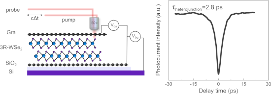
- (TMDs) through twist misalignment [18][19], which brings about fascinating physical phenomena [25][26][27][28][29]. Stacking semiconductor vdW materials with suitable bandgaps at specific angles not only breaks OOP symmetry, but also combines excellent semiconductor properties with spontaneous
- polarization, offering promising advances in optoelectronics [23][30]. One of the key optoelectronic phenomena in 2D semiconductor materials is the photocurrent response. The polarization, which results in spontaneous photocurrent under zero bias, gives rise to the bulk photovoltaic effect (BPVE), which can
- ) at room temperature. The electrical properties of the devices were characterized using an Agilent B1500 semiconductor analyzer in a Lake Shore vacuum chamber (10−4 Pa). SPCM and TRPC measurement The photocurrent maps were all obtained under zero bias using a custom-built scanning photocurrent


Mn-doped ZnO nanopowders prepared by sol–gel and microwave-assisted sol–gel methods and their photocatalytic properties
Beilstein J. Nanotechnol. 2024, 15, 1283–1296, doi:10.3762/bjnano.15.104
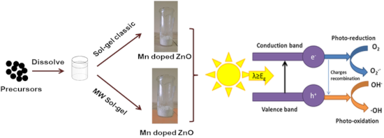
- generated CO2 were measured for both catalysts. These inexpensive semiconductor materials, which proved to be light-responsive, can be further used for developing water depollution technologies based on solar light energy. Keywords: microwave-assisted synthesis; oxalic acid mineralization; semiconductor
- semiconductor with many versatile and attractive applications in optical, optoelectronic, and photocatalytic fields [35][36][37]. The doping of ZnO with Mn can lead to the development of multifunctional nanostructures, such as room-temperature ferromagnetic materials with potential applications in spintronics
- catalyst is generally associated with low photocatalytic activity. Accordingly, various modifiers of semiconductor nanomaterials are used to enhance separation of the photogenerated charges, causing a corresponding decrease of PL emission. The correlation between photoluminescence and photocatalytic


Quantum-to-classical modeling of monolayer Ge2Se2 and its application in photovoltaic devices
Beilstein J. Nanotechnol. 2024, 15, 1153–1169, doi:10.3762/bjnano.15.94
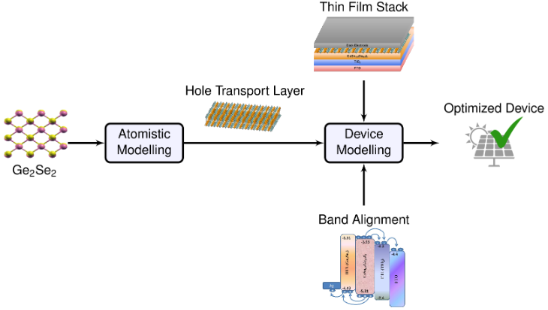
- . Figure 3 depicts that the monolayer Ge2Se2 is a direct-bandgap semiconductor with a bandgap of the order of 1.12 eV. Valence band maximum (VBM) and conduction band minimum (CBM) are located along the Γ-X path. The computed bandgap value and its dispersion nature are consistent with earlier reported works
- , ELUMO is the LUMO energy level. The ionization potential is calculated as IP = EVac − EHOMO, where IP, EVac, and EHOMO are ionization potential, vacuum energy level, and HOMO energy level, respectively. The electron affinity at a semiconductor surface is defined as the energy needed to carry an electron
- the proposed solar cell, we performed a numerical simulation using SCAPS-1D, which solves the fundamental semiconductor equations such as drift–diffusion, Poisson’s equation, and continuity equations as: and where and are the electron and hole current densities at the Fermi levels EFn and EFp





Photocatalytic methane oxidation over a TiO2/SiNWs p–n junction catalyst at room temperature
Beilstein J. Nanotechnol. 2024, 15, 1132–1141, doi:10.3762/bjnano.15.92
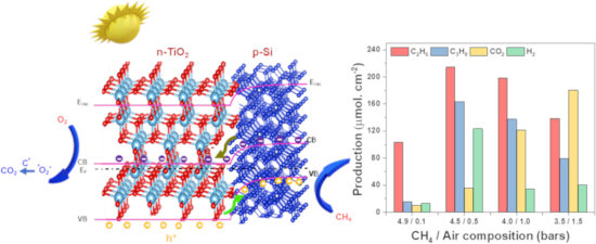
- deposition on catalyst surfaces [4][5][6][7]. Therefore, sustainable strategies for both green conversion and atmospheric removal of CH4 are urgently necessary [8][9][10][11]. Semiconductor-based photocatalysis has been attracting scientists’ attention because of its environmental friendliness and easy
- handling [12][13][14]. Photocatalytic metal oxide semiconductor materials have been utilized for converting solar energy into valuable chemical energy in the field of CH4 conversion [15][16][17]. Methane oxidation presents a particularly promising strategy. The primary objective is to convert methane into
- valuable products such as formaldehyde (HCHO), methanol (CH3OH), and other value-added oxygenates, which serve as essential precursors in various manufacturing and production processes [18][19]. The n-type semiconductor titanium dioxide (TiO2) has been discovered as a potential photocatalyst material


Unveiling the potential of alginate-based nanomaterials in sensing technology and smart delivery applications
Beilstein J. Nanotechnol. 2024, 15, 1077–1104, doi:10.3762/bjnano.15.88



Recent progress on field-effect transistor-based biosensors: device perspective
Beilstein J. Nanotechnol. 2024, 15, 977–994, doi:10.3762/bjnano.15.80
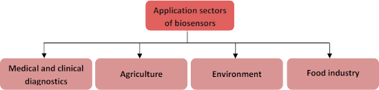
- increasing their use in daily life [38]. The first ion-sensitive field-effect transistor (IS FETs) biosensor combined the metal–oxide–semiconductor (MOS) structure with glass electrodes for measuring ion activities in electrochemical and biological environments [39]. Subsequently, hydrogen-sensitive MOSFET
- technology rapidly emerged [40][41]. However, all these FETs were highly bulky and required more space. Nakamoto et al. [42] later devised a biosensor with a novel fabrication method aligned well with the complementary metal–oxide–semiconductor (CMOS) fabrication process. Usually, biosensors convert
- biorecognition layer, a transducer, and an amplifier (Figure 2). It typically consists of a semiconductor channel and three terminal electrodes named drain, source, and gate [37][49]. The biorecognition layer selectively binds the target biomolecule (analyte), such as enzymes, antibodies, and proteins in a




Intermixing of MoS2 and WS2 photocatalysts toward methylene blue photodegradation
Beilstein J. Nanotechnol. 2024, 15, 817–829, doi:10.3762/bjnano.15.68
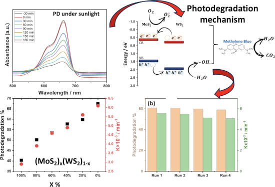
- ]. Typically, semiconductor-based photocatalysts, such as TiO2, ZnO2, and some other high-bandgap transition-metal dichalcogenides (TMD) have shown their ability to efficiently degrade the activated MB by irradiation [10][11]. Recently, TMD such as MoS2 and WS2, have displayed remarkable potential as
- cocatalysts. Their catalytic properties can be tailored based on their crystal structure, their surface area, and their morphology [12][13]. When TMD catalysts are intermixed, they form semiconductor–semiconductor junctions, enhancing their photocatalytic properties by promoting charge separation and electron


Effect of repeating hydrothermal growth processes and rapid thermal annealing on CuO thin film properties
Beilstein J. Nanotechnol. 2024, 15, 743–754, doi:10.3762/bjnano.15.62
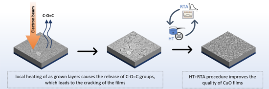
- devices. Keywords: CuO; hydrothermal method; rapid thermal annealing; thin films; Introduction Copper(II) oxide is a p-type semiconductor possessing a narrow bandgap, along with many beneficial electrical, optical, and magnetic properties. Particularly at the nanoscale, these properties set themselves
- × magnification. The spectral resolution was of the order of 0.5 cm−1. A 532 nm semiconductor laser was used to illuminate the samples. The measurements were performed without detection of polarization of the scattered light. A liquid nitrogen-cooled multichannel silicon CCD camera was used as a detector. Results




Level set simulation of focused ion beam sputtering of a multilayer substrate
Beilstein J. Nanotechnol. 2024, 15, 733–742, doi:10.3762/bjnano.15.61

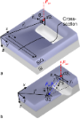
- possible to deterministically produce a nanoscale topography on the surface of almost any substrate [1]. FIB milling was originally established in semiconductor technology [2] and materials science applications [3]. Now it is increasingly used for fabrication of complex micro- and nanoscale structures and
- semiconductor heterostructures [13]. Metal and dielectric layers can be used as hard masks for achieving high resolution and throughput of the FIB nanofabrication process [14]. Modification of integrated circuits [15] is an industrially relevant application of multilayer structure processing. Effective

![[Graphic 55]](/bjnano/content/inline/2190-4286-15-61-i68.svg?max-width=637&scale=1.18182)


Elastic modulus of β-Ga2O3 nanowires measured by resonance and three-point bending techniques
Beilstein J. Nanotechnol. 2024, 15, 704–712, doi:10.3762/bjnano.15.58
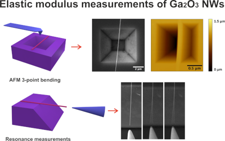
- geometry, utilising a 600 W Cu anode (Cu Kα radiation, λ = 1.5406 Å) X-ray tube. In four steps, (100)Si wafers (Semiconductor wafer, Inc.) with 50 nm thermal oxide, were processed to create the patterned silicon substrates with grooves and inverted pyramids. First, the patterns were created in a


Aero-ZnS prepared by physical vapor transport on three-dimensional networks of sacrificial ZnO microtetrapods
Beilstein J. Nanotechnol. 2024, 15, 490–499, doi:10.3762/bjnano.15.44
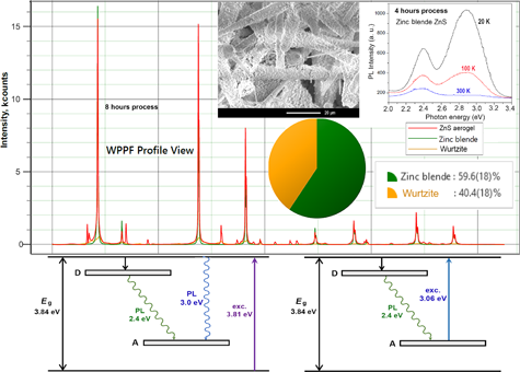
- metal oxides [1][9][10]. Metal oxides include TiO2, ZnO, Al2O3, WO3, Cu2O, CuO, SnO2, Fe2O3, Bi2O3, Ag3PO4, BiWO4, BiVO4, BiFeO3, and SeTiO3, while chalcogenides are represented by ZnS, ZnSe, CdS, PbS, CdSe, SnS2, and Bi2S3. Among porous semiconductor materials, recently developed super-lightweight ones
- for the preparation of the abovementioned semiconductor-based aeromaterials. Most of these aeromaterials have been produced by hydride vapor phase epitaxy (HVPE) [11][12][13][14][15][16][17][18]. Particularly, an aero-ZnS material exhibiting hydrophilic properties under tension and hydrophobic
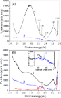
- recombination [35]. Therefore, the photoluminescence properties of the prepared aero-ZnS materials, including the near-bandgap emission, are similar to those inherent to semiconductor ZnS single crystals. The PL band around 2.4 eV is also excited by intraband-energy radiation with a wavelength of 405 nm (3.06



Heat-induced morphological changes in silver nanowires deposited on a patterned silicon substrate
Beilstein J. Nanotechnol. 2024, 15, 435–446, doi:10.3762/bjnano.15.39
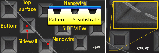
- silicon substrates with square holes were prepared from (100) silicon wafers (Semiconductor Wafer, Inc.) with 50 nm thermal oxide in four steps as follows: 1) conventional optical lithography process to produce the desired pattern in a photoresist on the wafer; 2) selective removal of SiO2 using buffered


Classification and application of metal-based nanoantioxidants in medicine and healthcare
Beilstein J. Nanotechnol. 2024, 15, 396–415, doi:10.3762/bjnano.15.36
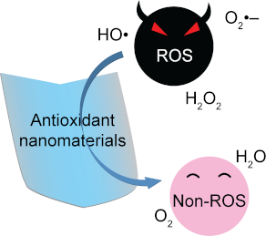
- ]. The heterostructures increase surface electron deficiency, redox couples, and oxygen vacancies through an intrinsic electric field and lattice mismatch at the metal–semiconductor interface. Thus, a high level of oxygen vacancies enhances the adsorption and activation of oxygen-containing ROS, that is



On the mechanism of piezoresistance in nanocrystalline graphite
Beilstein J. Nanotechnol. 2024, 15, 376–384, doi:10.3762/bjnano.15.34

- semiconducting grain boundaries can be considerably increased in the presence of strain. Hence, the asymmetric metallic grain boundaries undergo a metal–semiconductor transition in the presence of strain. This effect could open a way to utilize grain boundaries in graphene for fabricating highly sensitive


Investigating ripple pattern formation and damage profiles in Si and Ge induced by 100 keV Ar+ ion beam: a comparative study
Beilstein J. Nanotechnol. 2024, 15, 367–375, doi:10.3762/bjnano.15.33
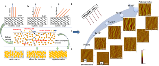
- performed on Si and Ge substrates. A correlation between ripple morphology and ion beam parameters was derived to understand the damage incurred by Ar+ ions inside both materials using RBS-c measurements. Experimental Details Commercially available Si and Ge wafers, procured from Semiconductor wafers Inc


Controllable physicochemical properties of WOx thin films grown under glancing angle
Beilstein J. Nanotechnol. 2024, 15, 350–359, doi:10.3762/bjnano.15.31
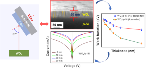
- fascinating optical and electrical properties [1]. WOx is a wide-bandgap oxide semiconductor with a large excitonic binding energy of 0.15 eV and a high optical absorption coefficient (≥104 cm−1 in the UV region) [2]. These, in conjunction with decent carrier mobility (12 cm2·V−1·s−1), make this material an
- -stoichiometric compositions and polymorphs, WOx usually behaves as an n-type semiconductor because an unintentional incorporation of a certain amount of reduced W cations is thermodynamically inevitable in these films [8]. It is, therefore, possible to tune the physicochemical properties, such as work function


Investigating structural and electronic properties of neutral zinc clusters: a G0W0 and G0W0Г0(1) benchmark
Beilstein J. Nanotechnol. 2024, 15, 310–316, doi:10.3762/bjnano.15.28
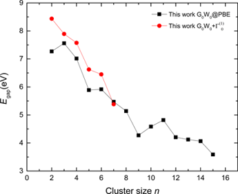
- functional theory (DFT) calculations at different levels of theory to study the transition states (vdW to semiconductor-like states) in Zn clusters. In addition, the approaches used to study the electronic properties, such as ionization potentials (IPs) of zinc, are based on the ∆-SCF methods; for some
- metal energy gap. Apart from this situation, for small-size clusters or nanoparticles, it is possible to observe quantum confinement effects resulting in an indeterminate bandgap, such as in the case of semiconductor clusters. As the size of the cluster decreases, the electronic energy levels become


![[Graphic 14]](/bjnano/content/inline/2190-4286-15-28-i15.svg?max-width=637&scale=1.18182)
Determining by Raman spectroscopy the average thickness and N-layer-specific surface coverages of MoS2 thin films with domains much smaller than the laser spot size
Beilstein J. Nanotechnol. 2024, 15, 279–296, doi:10.3762/bjnano.15.26
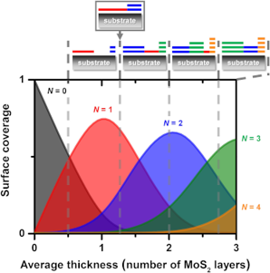
- transition to a direct bandgap semiconductor with very high photoluminescence quantum yield when thinned down to a monolayer [13][14][15][16][17]. Its unique electronic and optical properties could provide an edge in many future applications. The multilayers MoS2 structures are of the most common 2Hc type


Design, fabrication, and characterization of kinetic-inductive force sensors for scanning probe applications
Beilstein J. Nanotechnol. 2024, 15, 242–255, doi:10.3762/bjnano.15.23
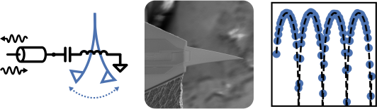
- etch rate of 10 μm/min. The isotropic etch results in an uneven clamping line, as shown in Figure 1g, leading to variations in the mechanical resonant frequency. Before the final etch and release step, we apply a Nitto Semiconductor Wafer Tape to the back side of the wafer, holding it together during



Ion beam processing of DNA origami nanostructures
Beilstein J. Nanotechnol. 2024, 15, 207–214, doi:10.3762/bjnano.15.20
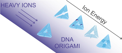
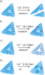
- regimes become the basis of commonly used material processing techniques such as high-energy ion implantation, widely applied in laser, detector, and semiconductor industries [30]. Finally, at low (keV) energies, the interaction of heavy ions is dominated by nuclear stopping, which is used in the most


CdSe/ZnS quantum dots as a booster in the active layer of distributed ternary organic photovoltaics
Beilstein J. Nanotechnol. 2024, 15, 144–156, doi:10.3762/bjnano.15.14
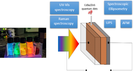
- –COOH groups, they can be easily labeled for chemical and biological applications. Low-molecular-weight organic molecules coat highly luminescent semiconductor nanocrystals. Materials and Methods Thin films, the intended active layers, were fabricated using the spin-coating method. The layers were a