Search results
Search for "atomic force microscopy" in Full Text gives 604 result(s) in Beilstein Journal of Nanotechnology. Showing first 200.
Hierarchically patterned polyurethane microgrooves featuring nanopillars or nanoholes for neurite elongation and alignment
Beilstein J. Nanotechnol. 2023, 14, 1157–1168, doi:10.3762/bjnano.14.96
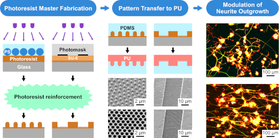
- uncrosslinked PDMS monomers (Supporting Information File 1, Figure S3C). Atomic force microscopy (AFM) scans of the samples (Figure 1F–H) show that the nanopillars and nanoholes have sub-micrometer feature sizes and a periodicity of around 1.2 µm. Due to AFM measurement artifacts, especially for lateral
- ) Cross-sectional profile of the flat (F), nanopillar (G), and nanohole (H) PU surface from atomic force microscopy scans, showing the dimensions of the nanostructures (G, H). (Dimensions in parentheses were obtained from SEM images in Supporting Information File 1, Figure S4.) (I) Water contact angles on
- microgroove (C), pillar–groove (D), and hole–groove (E) substrates, with corresponding high-magnification images (insets). (F–H) Cross-sectional profile of the microgroove (F), pillar–groove (G), and hole–groove (H) PU surface from atomic force microscopy scans, showing the dimensions of the structures. (I, J


Elasticity, an often-overseen parameter in the development of nanoscale drug delivery systems
Beilstein J. Nanotechnol. 2023, 14, 1149–1156, doi:10.3762/bjnano.14.95
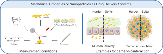
- article, we discuss examples highlighting the influence of elasticity in nanoscale biological interactions focusing on mucosal delivery and on tumor targeting. Besides this, we discuss the influence of different measurement settings using atomic force microscopy for the determination of mechanical
- properties of drug carriers. Keywords: atomic force microscopy; drug delivery; elasticity; mechanical properties; nanomedicine; nanoparticles; stiffness measurement; tissue/body distribution; Introduction Drug delivery systems are developed with the aim to transport a given drug to the site of action
- determine mechanical properties of nanoparticles (or their corresponding bulk materials) highlighting quartz crystal microbalance, rheology, and atomic force microscopy (AFM) are summarized by Li et al. [18]. Another often reported method is particle deformability, being extrusion a possibility for


A multi-resistance wide-range calibration sample for conductive probe atomic force microscopy measurements
Beilstein J. Nanotechnol. 2023, 14, 1141–1148, doi:10.3762/bjnano.14.94
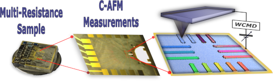
- work, we demonstrate the development of a multi-resistance reference sample for calibrating resistance measurements in conductive probe atomic force microscopy (C-AFM) covering the range from 100 Ω to 100 GΩ. We present a comprehensive protocol for in situ calibration of the whole measurement circuit
- : calibration; conductive probe atomic force microscopy; measurement protocol; nanoscale; resistance reference; Introduction Since its introduction thirty years ago by Murrell et al. [1], conductive probe atomic force microscopy (C-AFM) has evolved into a unique and powerful technique for measuring local


Spatial mapping of photovoltage and light-induced displacement of on-chip coupled piezo/photodiodes by Kelvin probe force microscopy under modulated illumination
Beilstein J. Nanotechnol. 2023, 14, 1059–1067, doi:10.3762/bjnano.14.87
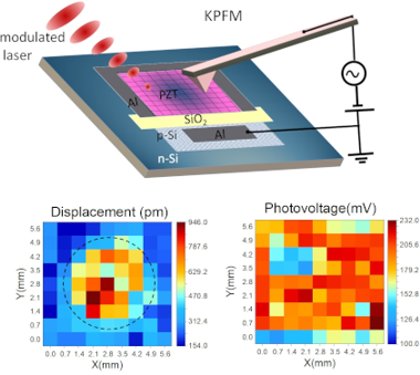
- mechanical oscillation of the piezoelectric membrane with vertical atomic resolution in real-time. This technique offers the opportunity to measure concurrently the optoelectronic and mechanical response of the device at the nanoscale. Furthermore, time-dependent atomic force microscopy (AFM) was employed to
- ]. However, the working principle of these techniques is based on optical interferometry mapping which can be challenging for light-sensitive devices. Furthermore, it can be advantageous to employ a method that also allows for mechanical contact and manipulation. Atomic force microscopy (AFM) [11][12][13][14
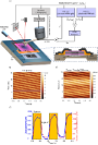


Exploring internal structures and properties of terpolymer fibers via real-space characterizations
Beilstein J. Nanotechnol. 2023, 14, 1004–1017, doi:10.3762/bjnano.14.83
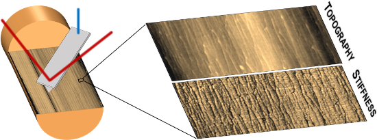
- Kevlar® K29 fibers, we find remarkable differences between the internal structures of the two fibers, and posit connections between our measurements and multifunctional performance studies from the literature. Keywords: atomic force microscopy; correlative characterization; high-performance fibers
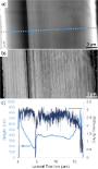
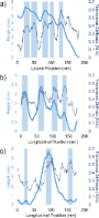
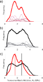
- , overcutting leads to transverse failures near the notches without producing an internal shear plane. Multifrequency atomic force microscopy scanning The exposed internal surfaces of FIB-notched fibers were scanned using a Cypher AFM with an ARC2 controller (Asylum Research). Olympus AC200TS cantilevers (k ≈ 9






Upscaling the urea method synthesis of CoAl layered double hydroxides
Beilstein J. Nanotechnol. 2023, 14, 927–938, doi:10.3762/bjnano.14.76
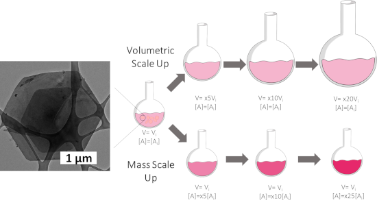
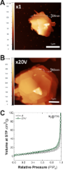
- CoAl-based LDH synthesis through an ARR method had been demonstrated, morphological aspects were addressed by means of scanning electron microscopy (SEM), transmission electron microscopy (TEM), and atomic force microscopy (AFM) (Figure 4 and Figure 5). For reference x1, well-defined hexagonal single
- microscope at an accelerating voltage of 20 kV. Atomic force microscopy (AFM) AFM was carried out with a Bruker Dimension Icon microscope in scan-assist-mode. A Bruker Scanasyst-Air silicon tip with a diameter of around 10 nm was used to obtain images with a resolution of 512 × 512 or 1024 × 1024 pixels. The


A graphene quantum dots–glassy carbon electrode-based electrochemical sensor for monitoring malathion
Beilstein J. Nanotechnol. 2023, 14, 701–710, doi:10.3762/bjnano.14.56
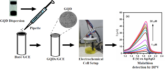
- hydrothermal process with glucose as a precursor undergoing carbonization. Different spectroscopic techniques were used to analyze the optical characteristics of GQDs, including UV–visible, photoluminescence, FTIR, and Raman spectroscopy. Atomic force microscopy, transmission electron microscopy, and X-ray


Humidity-dependent electrical performance of CuO nanowire networks studied by electrochemical impedance spectroscopy
Beilstein J. Nanotechnol. 2023, 14, 683–691, doi:10.3762/bjnano.14.54
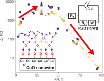
- electron microscopy (SEM, Hitachi S4800) and atomic force microscopy (AFM, Asylum Research MFP-3D). Electrochemical impedance measurements were performed under various atmospheric conditions in a custom-made system described elsewhere [28]. The main system parameters were RH from 4% to 97%, gas flow from
- . Atomic force microscopy: (g) a bundle of CuO nanowires between microelectrodes and (h) a height profile scan across the bundle. Impedance spectra measured for the system of CuO nanowire networks on microelectrodes at fixed T (30 °C) and various RH (5%, 20%, 50%, 73%, and 95%). Dotted lines connect


Suspension feeding in Copepoda (Crustacea) – a numerical model of setae acting in concert
Beilstein J. Nanotechnol. 2023, 14, 603–615, doi:10.3762/bjnano.14.50
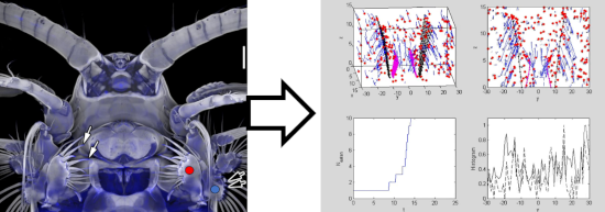
- -resolution CLSM imaging or atomic force microscopy. As it was visualized by CLSM [55][56][57], the basal parts of some short and long setae appear to be relatively soft and seem to contain resilin or other proteins. This should influence the mobility of the rotating setae. To account for this in the


SERS performance of GaN/Ag substrates fabricated by Ag coating of GaN platforms
Beilstein J. Nanotechnol. 2023, 14, 552–564, doi:10.3762/bjnano.14.46
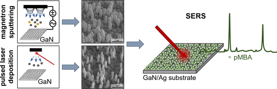
- substrates fabricated using both methods, we attempted to prepare substrates with a comparable amount of deposited Ag, which was examined and controlled using atomic force microscopy (AFM). For this purpose, additional Ag layers were deposited on flat Si substrates. Based on the measured thickness of the Ag


Carbon nanotube-cellulose ink for rapid solvent identification
Beilstein J. Nanotechnol. 2023, 14, 535–543, doi:10.3762/bjnano.14.44
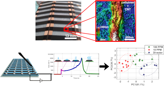
- length of 5 μm were produced at CTNano/UFMG [59][60][61]. Morphological analysis was carried out by scanning electron microscopy (SEM) in a Quanta 200 FEG, using secondary electrons between 2 and 10 kV. Atomic force microscopy (AFM) was carried out on a Bruker MultiMode8 SPM using the intermittent


On the use of Raman spectroscopy to characterize mass-produced graphene nanoplatelets
Beilstein J. Nanotechnol. 2023, 14, 509–521, doi:10.3762/bjnano.14.42
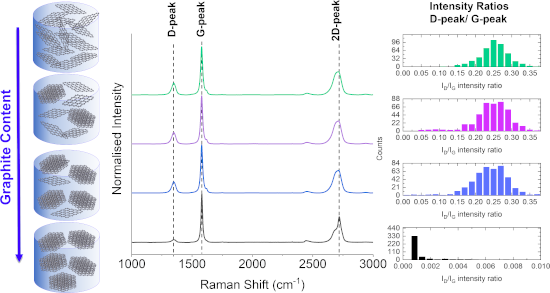
- widely used characterization tool for GR2Ms [8]. A search of Web of Science showed that of 97,532 articles published in the last five years with “Graphene” in the abstract, 9.3% also mentioned “Raman”. This is compared with atomic force microscopy (AFM) (2.4%), scanning electron microscopy (SEM) (11.4


High–low Kelvin probe force spectroscopy for measuring the interface state density
Beilstein J. Nanotechnol. 2023, 14, 175–189, doi:10.3762/bjnano.14.18
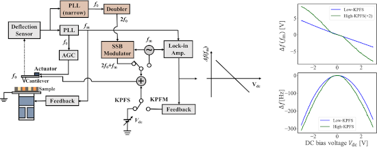
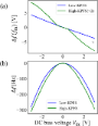
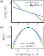
- known as a method that can measure the contact potential difference (CPD) between a tip and a sample with high spatial resolution [4][5]. KPFM is based on the detection of the electrostatic force between a tip and a sample using atomic force microscopy (AFM) [6][7][8]. CPD and topographic measurements



Structural, optical, and bioimaging characterization of carbon quantum dots solvothermally synthesized from o-phenylenediamine
Beilstein J. Nanotechnol. 2023, 14, 165–174, doi:10.3762/bjnano.14.17
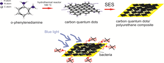
- 2.2 mg/mL. These specimens were designated as CQDs/PU. For bioimaging studies, toluene was evaporated, and a thin film of CQDs was redissolved in water and filtered. The prepared QCD samples were characterized by transmission electron microscopy (TEM), atomic force microscopy (AFM), Fourier


Intermodal coupling spectroscopy of mechanical modes in microcantilevers
Beilstein J. Nanotechnol. 2023, 14, 123–132, doi:10.3762/bjnano.14.13
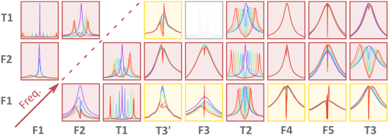
- Ioan Ignat Bernhard Schuster Jonas Hafner MinHee Kwon Daniel Platz Ulrich Schmid Institute of Sensor and Actuator Systems, TU Wien, Gußhaustraße 27–29, 1040 Vienna, Austria 10.3762/bjnano.14.13 Abstract Atomic force microscopy (AFM) is highly regarded as a lens peering into the next discoveries
- . Through such findings we aim to expand the field of multifrequency AFM with innumerable possibilities leading to improved signal-to-noise ratios, all accessible with no additional hardware. Keywords: atomic force microscopy; intermodal coupling; nonlinear mechanics; optomechanics; sideband cooling
- ; Introduction Atomic force microscopy has established itself as one of the most powerful tools in nanotechnology. With meticulous setups amassing techniques such as ultra high vacuum, cryogenic temperatures, and CO-terminated tips, it is able to create a wonderful vista of surfaces, not missing the atoms for


Liquid phase exfoliation of talc: effect of the medium on flake size and shape
Beilstein J. Nanotechnol. 2023, 14, 68–78, doi:10.3762/bjnano.14.8
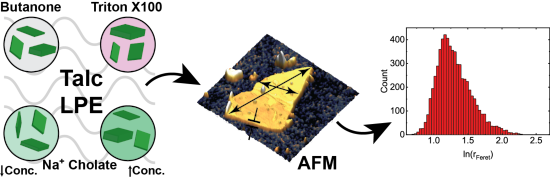
- based on atomic force microscopy images of thousands of flakes, the shape and size distribution of nanotalc obtained using the four different media are compared. This comparison highlights the strengths and weaknesses of the media tested and hopefully will facilitate the choice of the medium for
- applications that have specific requirements. Keywords: 2D materials; atomic force microscopy; liquid phase exfoliation; nanomaterials; talc; Introduction Two-dimensional (2D) materials have attracted a lot of interest due to their outstanding properties [1]. However, large-scale production is still a
- solution, and butanone. The mechanical energy necessary to delaminate the mineral was provided by an ultrasonic bath. We report a statistical analysis of the dimensions (measured by atomic force microscopy) of the nanoflakes obtained employing the four routes, evidencing that the exfoliation medium has an



Gap-directed chemical lift-off lithographic nanoarchitectonics for arbitrary sub-micrometer patterning
Beilstein J. Nanotechnol. 2023, 14, 34–44, doi:10.3762/bjnano.14.4
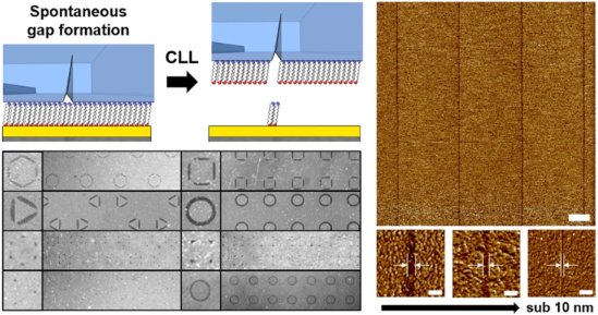
- force microscopy (Dimension Fastscan, Bruker Nano Surfaces, Hsinchu, Taiwan). Results and Discussion The results of selective SAM removal are visualized by backfilling biotinylated alkanethiol (BAT) molecules into the post lift-off regions followed by conjugating streptavidin and FITC-labeled anti
- to etch the exposed underlying Au film. After 30 min of etching, the substrate was rinsed with deionized water and blown dry with nitrogen gas. The transferred metal structures were then characterized by optical microscopy, scanning election microscopy (SEM, JEOL JSM-7600F, Tokyo, Japan) and atomic


From a free electron gas to confined states: A mixed island of PTCDA and copper phthalocyanine on Ag(111)
Beilstein J. Nanotechnol. 2022, 13, 1572–1577, doi:10.3762/bjnano.13.131
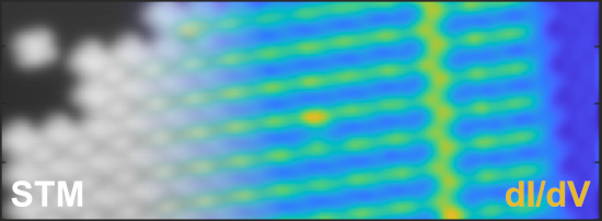
- -precision STM and atomic force microscopy (AFM) scanning. Third, CuPc and PTCDA are known to form commensurate phases on flat metal surfaces. In particular, they have been well studied at different stoichiometries on Ag(111) [16]. Henneke and co-workers showed that more than 0.15 ML of PTCDA in addition to


Induced electric conductivity in organic polymers
Beilstein J. Nanotechnol. 2022, 13, 1551–1557, doi:10.3762/bjnano.13.128
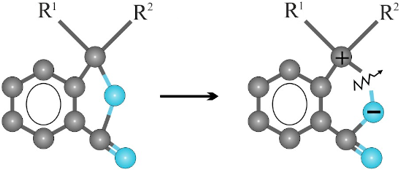
- atomic force microscopy. In some cases, it was possible to observe regions with surface macromolecular (quasicrystalline) ordering [7]. The remarkable property of PDP is that, depending on the length of certain atomic bonds, its molecule can exist in several spatial configurations. Under normal
- , associates of macromolecules are formed in the solution, and the influence of adhesion processes decreases, but the cohesive forces increase. In the entire thickness range from 3 nm to 1 µm, the films are solid, without significant defects and/or pin holes. The polymer films were studied by atomic force
- microscopy (AFM) using an earlier described methodology [5]. The study of the film morphology showed that they are homogeneous, and within the entire thickness range from 3 nm to 1 µm the films are solid, without significant defects and/or pin holes. The observation confirms the good film-forming properties



Frequency-dependent nanomechanical profiling for medical diagnosis
Beilstein J. Nanotechnol. 2022, 13, 1483–1489, doi:10.3762/bjnano.13.122
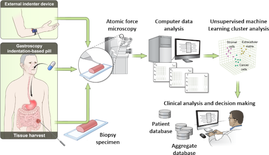
- Bioengineering, National Institutes of Health, Bethesda, Maryland, USA 10.3762/bjnano.13.122 Abstract Atomic force microscopy (AFM), developed in the early 1980s, has become a powerful characterization tool in micro- and nanoscale science. In the early 1990s, its relevance within biology and medicine research
- mechanical changes in the affected tissues. Keywords: atomic force microscopy; healthcare; mechanical properties; mechanobiology; medical diagnosis; Introduction Since its invention in the early 1980s, atomic force microscopy (AFM) has been extensively used for topographical, mechanical, electrical, and


Laser-processed antiadhesive bionic combs for handling nanofibers inspired by nanostructures on the legs of cribellate spiders
Beilstein J. Nanotechnol. 2022, 13, 1268–1283, doi:10.3762/bjnano.13.105
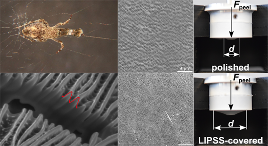
- Microsoft Excel. Details are presented in Table S2 in Supporting Information File 1. To investigate the effects of the surface texture on the measured peel-off force in more detail, the surfaces of the Al alloy and the Ti alloy samples were investigated by means of atomic force microscopy (AFM). The






Studies of probe tip materials by atomic force microscopy: a review
Beilstein J. Nanotechnol. 2022, 13, 1256–1267, doi:10.3762/bjnano.13.104
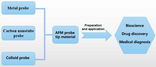
- a homemade cantilevered non-contact atomic force microscopy (NC-AFM) system. As the first step of tip sharpening, the focus is on the controlled extraction of individual clusters. The experimental results show that controlled extraction of individual clusters induces a change in tip sharpness, which
- future, such probes will enable previously unexplored conductivity measurements, such as measurements of semiconductor nanostructures or electrical conductivity on insulating substrates. Conductive atomic force microscopy (C-AFM) can be used to characterize the electrical properties of semi-conductive
Design of surface nanostructures for chirality sensing based on quartz crystal microbalance
Beilstein J. Nanotechnol. 2022, 13, 1201–1219, doi:10.3762/bjnano.13.100
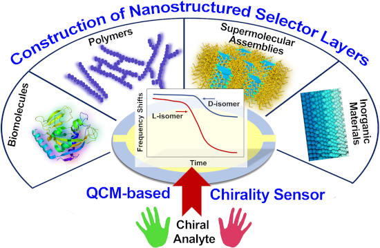
- , Xu et al. studied real-time chiral recognition of CD films to isomers in the gas phase [69]. Based on atomic force microscopy (AFM) observations, functional β-CDs with a short sulfide group were inclined to form monolayers. In contrast, those with long sulfide groups produced a quasi-two-layer


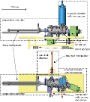
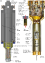
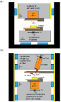
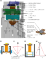
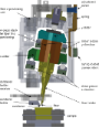
A cantilever-based, ultrahigh-vacuum, low-temperature scanning probe instrument for multidimensional scanning force microscopy
Beilstein J. Nanotechnol. 2022, 13, 1120–1140, doi:10.3762/bjnano.13.95
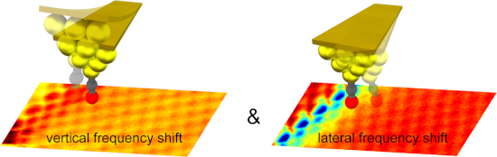
- Cantilever-based atomic force microscopy (AFM) performed under ambient conditions has become an important tool to characterize new material systems as well as devices. Current instruments permit robust scanning over large areas, atomic-scale lateral resolution, and the characterization of various sample
- , but also perform rapid overview scans with the tip kept at larger tip–sample distances for robust imaging. Keywords: atomic force microscopy; atomic resolution; instrumentation design; multimodal operation; ultrahigh vacuum; Introduction Atomic force microscopy (AFM) operated under vacuum or





Effects of focused electron beam irradiation parameters on direct nanostructure formation on Ag surfaces
Beilstein J. Nanotechnol. 2022, 13, 1004–1010, doi:10.3762/bjnano.13.87
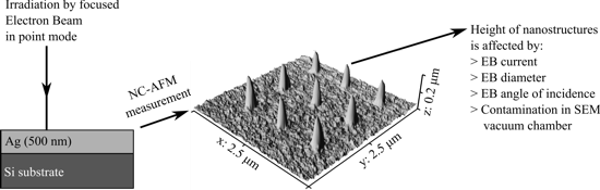
- surfaces undergoing irradiation by a focused electron beam. Keywords: atomic force microscopy; electron beam; lithography; nanostructure; silver; sputtering; surface; Introduction Metallic nanostructures have various uses, including in nano-electro-mechanical systems [1], plasmonic biosensors [2], and
- -contact atomic force microscopy (AFM) using the model Park NX10 AFM. The first experiment was conducted with beam current I as the variable parameter ranging from 7 to 500 pA. However, changing the value of I also changed the beam diameter d, which is a function of I and the working distance (WD). The
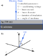
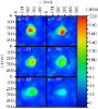
- kV, I = 42 pA, d = 14 nm, and t = 60 s. Atomic force microscopy images of the nanostructures on an Ag surface as a function of the angle of incidence of the electron beam. Constant EB parameters are: U = 30 kV, I = 42 pA, d = 14 nm, and t = 60 s. The volume and height of the nanostructures on an Ag