


Search results
Search for "nanopillar" in Full Text gives 23 result(s) in Beilstein Journal of Nanotechnology.
He+ FIBID-fabricated 3D AFM tip architectures: an exploratory study of hollow pillars, helices, and spirals
Beilstein J. Nanotechnol. 2026, 17, 863–871, doi:10.3762/bjnano.17.62
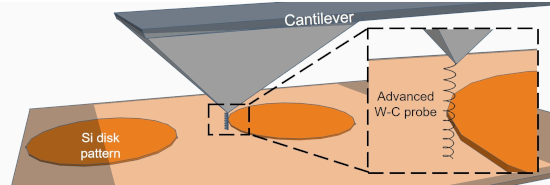
- required. Keywords: 3D-printed tips; AFM tips; beam induced nanomanufacturing; focused ion beam induced deposition (FIBID); helium ion microscope; nanohelix; nanopillar; nanospiral; scanning tip microscopy; surface topography; tungsten carbide; Introduction The atomic force microscope (AFM) is a
- the vacuum system. Such methods have enabled the direct fabrication of functional nanostructures on a range of substrates, including AFM cantilevers. FEBID and FIBID have already been used to fabricate AFM nanopillar-type tips, most commonly from carbon- [12], cobalt- [13], iron- [14], platinum- [15
- μm and an approximate tip radius of 23 nm. Nanopillar structures span a broader height range, from 0.22 to 3.19 μm, with a similar tip radius of about 23 nm. Nanospiral tips are shorter, with heights between 0.05 and 0.22 μm, and exhibit a smaller approximate tip radius of 15 nm. Because of the


Current status of using adsorbent nanomaterials for removing microplastics from water supply systems: a mini review
Beilstein J. Nanotechnol. 2025, 16, 1837–1850, doi:10.3762/bjnano.16.127
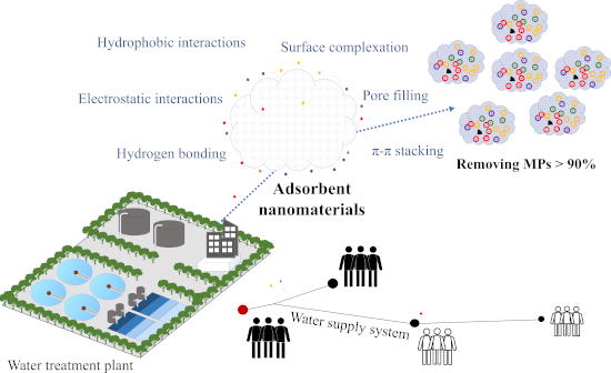
- (pore sizes of 0.3–3.4 nm) and adsorbed MPs through coordination and hydrophobic interactions [60]. Haris et al. introduced a magnetic C@FeO nanopillar adsorbent on a 2D-MOF, achieving approximately 100% removal of MPs (sizes <5 μm) after 1 h, significantly faster than conventional methods [61


Electron beam-based direct writing of nanostructures using a palladium β-ketoesterate complex
Beilstein J. Nanotechnol. 2025, 16, 530–539, doi:10.3762/bjnano.16.41
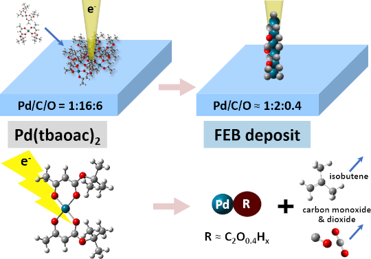
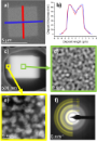
- high-aspect ratio nanopillars as reported for [Cu(tbaoac)2] [31]. Nanopillar with [Pd(tbaoac)2] A nanopillar was grown with [Pd(tbaoac)2] by FEBID and a beam current of 700 pA at 20 keV with a substrate temperature of 70 °C and a GIS temperature of 85 °C, as shown in Figure 5. We observed the formation
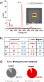
- from the primary electron beam [52]. The deposition rate is 0.23 nm·s−1. The volume growth rate for the nanopillar neglecting the granular deposit would be 0.019 µm3·min−1, while for the square deposit in Figure 2a it is 0.032 µm3·min−1. In general, we expect the volume growth rate to be identical
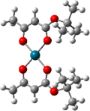
- of further studies of dissociation and desorption mechanisms involved in the removal of the carbon- and oxygen-rich ketoesterate ligands. The nanopillar formed from this precursor demonstrates its potential for 3D nanostructure fabrication using FEBID. The structure of bis(tert-butylacetoacetate


Hierarchically patterned polyurethane microgrooves featuring nanopillars or nanoholes for neurite elongation and alignment
Beilstein J. Nanotechnol. 2023, 14, 1157–1168, doi:10.3762/bjnano.14.96
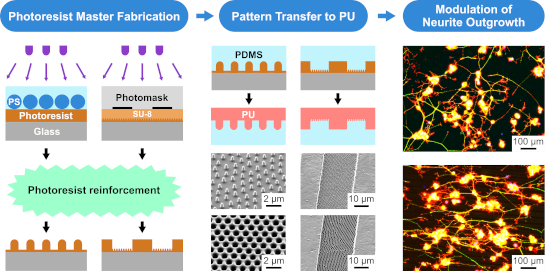
- demonstrates a promising method for the creation of hierarchical nano-/microstructures on various polymers for nerve implant applications. Results and Discussion Fabrication and characterization of PU nanopillar and nanohole substrates We first fabricated nanopillar and nanohole arrays on medical-grade
- nanopillar array on an SU-8 film (Figure 1A(i) and (ii)). SU-8 generates a strong acid in UV-exposed areas, which, in turn, undergo acid-initiated crosslinking during the post-exposure baking step [18]. However, we found that the subsequent formation of a polydimethylsiloxane (PDMS) inverse mold from the SU
- -8 nanopillar array fails due to the breakage of the brittle SU-8 nanopillars (Supporting Information File 1, Figure S1A,B), while further hard-baking to strengthen pillar adhesion causes SU-8 reflow, resulting in a dramatic decrease in the pillar aspect ratio (Supporting Information File 1, Figure


A super-oscillatory step-zoom metalens for visible light
Beilstein J. Nanotechnol. 2022, 13, 1220–1227, doi:10.3762/bjnano.13.101
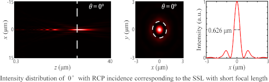
- potential applications in the field of super-resolution microscopic imaging and optical precision machining. The layout of the double-layer step-zoom metalens. Phase profiles of the front and rear metasurfaces for (a) short and (b) long focal lengths. (a) Schematic of a TiO2 rectangular nanopillar. (b


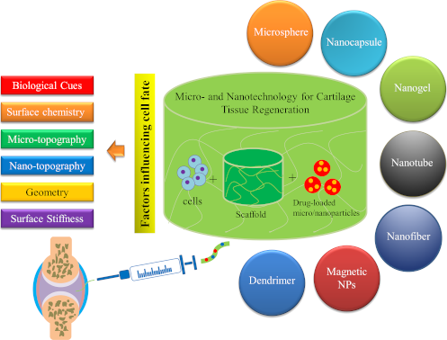
Micro- and nanotechnology in biomedical engineering for cartilage tissue regeneration in osteoarthritis
Beilstein J. Nanotechnol. 2022, 13, 363–389, doi:10.3762/bjnano.13.31


A review of defect engineering, ion implantation, and nanofabrication using the helium ion microscope
Beilstein J. Nanotechnol. 2021, 12, 633–664, doi:10.3762/bjnano.12.52
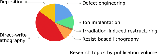
- focused helium ion beam of the HIM. Wang et al. used the HIM to conduct a systematic study of the effect of such a helium gas bubble superlattice on the mechanical properties of copper, which is representative of a range of fcc alloys that are known to exhibit radiation tolerance [78]. Copper nanopillar


Bio-imaging with the helium-ion microscope: A review
Beilstein J. Nanotechnol. 2021, 12, 1–23, doi:10.3762/bjnano.12.1
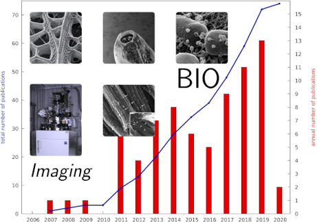
- nanopillar texture on the wing of a dragonfly Orthetrum villosovittatum was studied. In addition to imaging the wing alone, samples were prepared with E. coli bacteria on them, to study the bactericidal properties of the nanostructure. Along similar lines, the nanostructures on the wings of three different


Optically and electrically driven nanoantennas
Beilstein J. Nanotechnol. 2020, 11, 1542–1545, doi:10.3762/bjnano.11.136
- boosted by forming a hybrid antenna. In the case of [55] an AlGaAs nanopillar, which has an anapole mode resonant with the pump wavelength, is encompassed by a gold ring. The field enhancement by the plasmonic structure is shown to lead to almost two orders of magnitude improvement of the SHG and a
Hexagonal boron nitride: a review of the emerging material platform for single-photon sources and the spin–photon interface
Beilstein J. Nanotechnol. 2020, 11, 740–769, doi:10.3762/bjnano.11.61
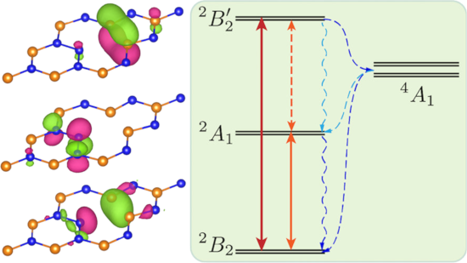
- the nanopillar substrate method, and SPEs have a similar PL distribution of the strain-induced emitters and brightness comparable to the brightest SPEs found in h-BN. Neutron irradiation [127] shows a homogenous distribution of emitters within the 2D h-BN multilayers and the density of induced color




Deterministic placement of ultra-bright near-infrared color centers in arrays of silicon carbide micropillars
Beilstein J. Nanotechnol. 2019, 10, 2383–2395, doi:10.3762/bjnano.10.229
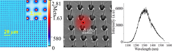
- nanopillar with optical pump saturation occurring at 3.5 mW has been shown previously [48]. This corresponds to a fluorescence enhancement (FE) by a factor of two to three compared to single emitters in non-fabricated samples. Thus, for sample 1 we estimate in the gap about ca. 41 emitters, assuming a count


Nitrogen-vacancy centers in diamond for nanoscale magnetic resonance imaging applications
Beilstein J. Nanotechnol. 2019, 10, 2128–2151, doi:10.3762/bjnano.10.207
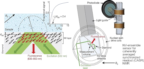
- attaching it to the tip of an atomic force microscope (AFM). This can also be achieved by mounting a high-purity diamond nanopillar on an AFM with an NV center placed 10 nm from its end, achieving a sensitivity of 56 nT·Hz−1/2, as reported in [37]. Nanodiamond scanning tips currently suffer from a
- statistical process to integrate the NV in the tips. This limits the applications due to excessive complex and non-scalable fabrication procedures, based on nanoscale manipulations [38]. A more promising approach [39] relies on generating an NV center less than 20 nm below the surface in a diamond nanopillar
- mounted on a thin platform, typically of less than 1 μm thickness. Coupled with the nanopillar, this diamond film makes a scanning probe when mounted to an AFM head. It is expected that this method can enhance the photoluminescence collected from the NV by a factor of 10. Finally, ND embedded in a living


Controlling surface morphology and sensitivity of granular and porous silver films for surface-enhanced Raman scattering, SERS
Beilstein J. Nanotechnol. 2018, 9, 2813–2831, doi:10.3762/bjnano.9.263
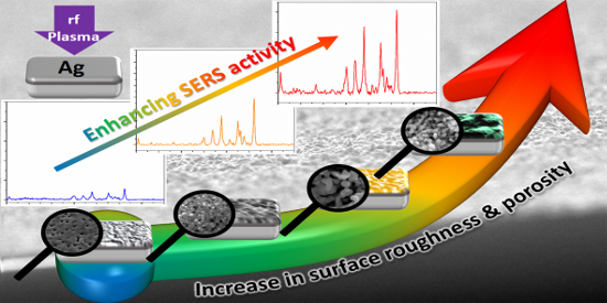
- ][27][28][29][30][31][32][33][34]. Additional methods appeared in which nanoparticles or metal films are deposited on structured substrates as carbon nanotubes [35][36][37][38][39], graphene foam [40], nanorod or nanopillar arrays [41][42], biological scaffolds [43][44], black silicon [45][46





Metal–dielectric hybrid nanoantennas for efficient frequency conversion at the anapole mode
Beilstein J. Nanotechnol. 2018, 9, 2306–2314, doi:10.3762/bjnano.9.215
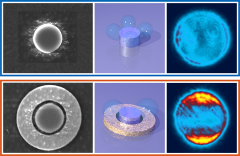
- antenna based on an AlGaAs nanopillar surrounded by a gold ring, which merges in a single platform the strong field confinement typically produced by plasmonic antennas with the high nonlinearity and low loss characteristics of dielectric nanoantennas. This platform allows enhancing the coupling of light
- to the nanopillar at coincidence with the anapole mode, hence boosting both second- and third-harmonic generation conversion efficiencies. More than one order of magnitude enhancement factors are measured for both processes with respect to the isolated structure. Conclusion: The present results
- nanopillar with nominal radius r1 = 410 nm, height h = 200 nm and gap size g1 ≈ 100 nm as shown in Figure 1c, while type 2 features a nanopillar radius r2 = 380 nm with the same height and a gap size g2 = 200 nm (not shown). The geometrical parameters of the Au ring in both cases are w = 410 nm and h = 80 nm




A novel copper precursor for electron beam induced deposition
Beilstein J. Nanotechnol. 2018, 9, 1220–1227, doi:10.3762/bjnano.9.113
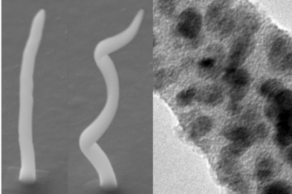
- pads together with the standard deviation. (c) Real and (d) imaginary part of the Maxwell–Garnett model. The model uses the dielectric function of copper from [24], and of carbon from [23]. The dotted lines are the measured values. (a + b) Scanning electron micrographs of a single nanopillar (a) and a


Magnetic characterization of cobalt nanowires and square nanorings fabricated by focused electron beam induced deposition
Beilstein J. Nanotechnol. 2018, 9, 1040–1049, doi:10.3762/bjnano.9.97
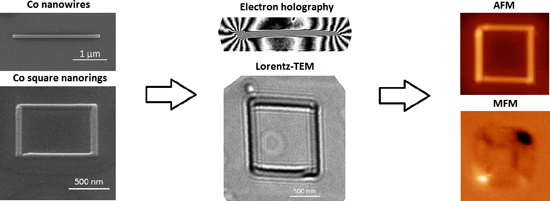
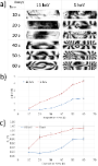
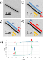
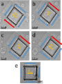
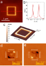
- imperfection caused by the limitations of our scanning setup. This flaw is similar to the one previously mentioned, and can be regarded as a small magnetic nanopillar causing a local magnetization rearrangement along the side [44]. This, however, does not seem to perturb the overall magnetic onion state, which
Mechanistic insights into plasmonic photocatalysts in utilizing visible light
Beilstein J. Nanotechnol. 2018, 9, 628–648, doi:10.3762/bjnano.9.59
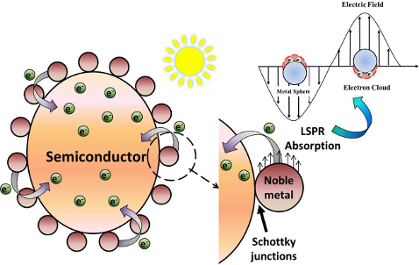
- effect) with Au or Ag, (considered to induce an enhanced plasmonic effect) in which the former acts as an electron sinker for more efficient electron–hole pair separation [6]. For instance, Shuang et al. studied one such combination where they decorated TiO2 nanopillar arrays with both Au and Pt NPs and





Direct writing of gold nanostructures with an electron beam: On the way to pure nanostructures by combining optimized deposition with oxygen-plasma treatment
Beilstein J. Nanotechnol. 2017, 8, 2530–2543, doi:10.3762/bjnano.8.253
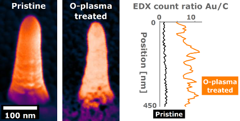
- of the topmost tip of the nanopillar is plagued by the small self-absorption of the carbon K-line in the tip region and the depth-dependence of the absorption in tapered tip geometries. We would like to point out that a thickness-dependent error for the given results still exists, so the measured
- axis (FSA) and slow scanning axis (SSA), can be adjusted relative to the gas flux vector (GFV). (b) SEM image (45° tilt) of a Au nanopillar (NP) fabricated by FEBID. (c) TEM image of a FEBID Au NP, with the corresponding electron diffraction pattern given in the inset, confirming the polycrystalline

A top-down approach for fabricating three-dimensional closed hollow nanostructures with permeable thin metal walls
Beilstein J. Nanotechnol. 2017, 8, 1231–1237, doi:10.3762/bjnano.8.124
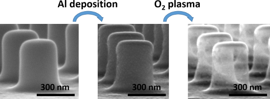
- and near-vertical or slightly positive leaning sidewalls. The latter is a consequence of proximity effects and the negative character of the resist. Then, a thin film of Al (thickness on the horizontal surface of 40 nm) is deposited by evaporation on the SU-8 nanopillar array (Figure 1b). The
- nanopillar slope favors metal deposition on the sidewalls, as evidenced by the granular appearance of these surfaces. Finally, an oxygen-plasma treatment is applied to the structure leading to the result shown in Figure 1c. The pillars look transparent to the electron beam, revealing the thinness of the Al
- previous work [11], the SU-8 nanopillar array reflectance exhibits two dips: at λ ≈ 640 nm, due to a metal-assisted, guided mode resonance (MaGMR), and at λ ≈ 840 nm, due to a surface plasmon polariton (SPP). Both of these dips are related to the Al layer (Si substrate coating) of thickness 100 nm on which


Localized surface plasmon resonances in nanostructures to enhance nonlinear vibrational spectroscopies: towards an astonishing molecular sensitivity
Beilstein J. Nanotechnol. 2014, 5, 2275–2292, doi:10.3762/bjnano.5.237
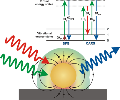
- distinct plasmon resonances, a transverse and a longitudinal mode, nano-antennas have been shown to allow large amplification of molecular signals. In 2000, Baldelli et al. demonstrated that strong enhancements of the SFG signal could be obtained through exciting the plasmon mode in a nanopillar array [76
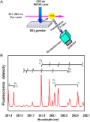
- (Figure 7b,c). In 2011, Lis et al. reported the enhancement of an alkanethiol SAM on randomly distributed gold nanopillars vertically-aligned on either a flat platinum or gold surface (Figure 8a) [77]. The authors achieved a selective excitation of the nanopillar LSPR modes by tuning the visible frequency




Cyclic photochemical re-growth of gold nanoparticles: Overcoming the mask-erosion limit during reactive ion etching on the nanoscale
Beilstein J. Nanotechnol. 2013, 4, 886–894, doi:10.3762/bjnano.4.100
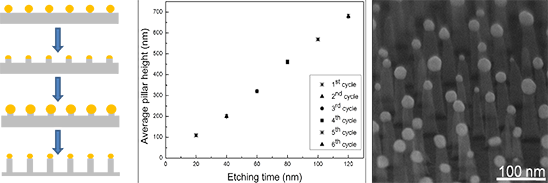
- compensating for the erosion due to the previous cycle. As a result of this mask repair method, arrays of silica nanopillar with heights up to 680 nm and aspect ratios of 10:1 are fabricated. Based on the given recipes, the approach can be applied to a variety of materials like silicon, silicon oxide, and
- was analyzed by a self-made contact angle measurement system with a droplet volume of typically 10 µL. Schematics of nanopillar fabrication by applying Au NP as masks after fine tuning their size by an UV-light activated photochemical process. To stabilize the NP positions during the growth process
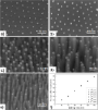
- nm). Panel (c) presents the size distributions of the seeding steps defined in panel (d), which includes the corresponding seeding times. Nanopillar arrays etched into silica applying Au NP of different diameters as masks: (a) NP diameter = 12 nm, pillar height = 50 nm (averages), (b) NP diameter


Controlled positioning of nanoparticles on a micrometer scale
Beilstein J. Nanotechnol. 2012, 3, 773–777, doi:10.3762/bjnano.3.86
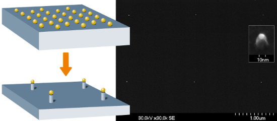
- nanopillar with residual Au mask as cap. SEM image of four squares of nanopillars as obtained after RIE with single Au NPs, arranged in a square, as etching masks (step 5 in Figure 2). Distance between pillars: 1.2 μm. Acknowledgement The continuous financial support by German Science Foundation (DFG


Focused electron beam induced deposition: A perspective
Beilstein J. Nanotechnol. 2012, 3, 597–619, doi:10.3762/bjnano.3.70
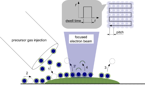
- . Che et al. reported on FEBID of FePt nanopillar structures by using Fe(CO)5 and Me3Pt(IV)CpMe as precursor gases in parallel [27]. The originally amorphous deposits were shown to crystallize into the L10 “face-centered tetragonal” structure of FePt after an in situ annealing step at 600 °C. The





