Search results
Search for "scanning electron microscopy" in Full Text gives 779 result(s) in Beilstein Journal of Nanotechnology. Showing first 200.
Nanoglasses: a trail towards uncharted regions of vitreous materials and their properties?
Beilstein J. Nanotechnol. 2026, 17, 1047–1062, doi:10.3762/bjnano.17.72
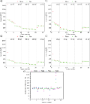
- a transmission electron microscope (TEM), so that projection artefacts that are inherent in the analysis of powder-compacted nanoglasses can be avoided. Figure 3a presents a scanning electron microscopy (SEM) overview of the columnar nanoglass thin films, highlighting their overall structural


Influence of an external electric field on the catalytic CO oxidation of nanoscaled CeO2 and its La3+ and Gd3+ congeners
Beilstein J. Nanotechnol. 2026, 17, 1028–1038, doi:10.3762/bjnano.17.70
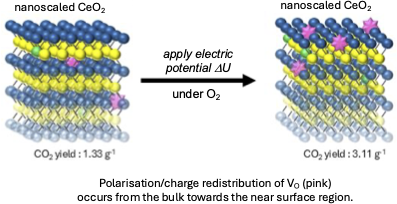
- Information File 1, Figures S20–S24). All cerium oxide nanoparticles are strongly aggregated and form dense strongly corrugated films with an agglomerated particle size of about 50 nm in scanning electron microscopy (SEM) (Supporting Information File 1, Figure S25). Transmission electron microscopy (TEM) and


Synthesis and characterization of RF-sputtered ZnTe/Cu2−xTe thin films for solar cell applications
Beilstein J. Nanotechnol. 2026, 17, 1016–1027, doi:10.3762/bjnano.17.69
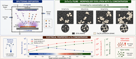
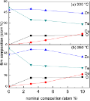
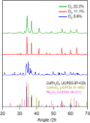
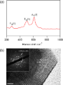
- produced only minor lattice modifications, while higher Cu and O contents promoted the formation of Cu2−xTe secondary phases, as confirmed by Raman spectroscopy, grazing-incidence X-ray diffraction and scanning electron microscopy. Optical measurements showed a significant reduction in infrared
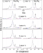
- . Vibrational and structural surface properties Figure 4 shows Raman spectra and a scanning electron microscopy (SEM) image of the CuZnTeO film grown at 300 °C with a nominal Cu and O concentration of 3 atom %. The SEM image reveals an irregular surface morphology characterized by agglomerate formation with non



Ultrasonic irradiation in the synthesis of nanohydroxyapatite: a chemically friendly technique for improving hemocompatibility and antibiofilm applications
Beilstein J. Nanotechnol. 2026, 17, 991–1015, doi:10.3762/bjnano.17.68
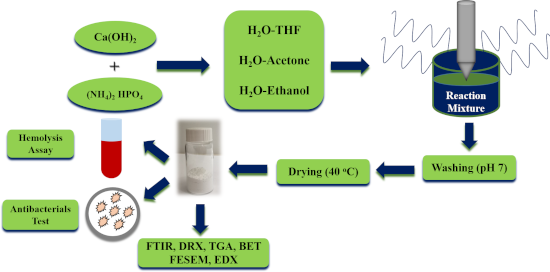
- quantitative analysis of particle size was conducted using field-emission scanning electron microscopy (FESEM) and BET surface area measurements. These findings, along with their corresponding statistical evaluations, are presented and extensively discussed in section “Field emission scanning electron
- only undergoes transformations leading to its decomposition at temperatures above 1000 to 1300 °C; this promotes the formation of other biocompatible phosphate species, such as tetracalcium phosphate and tricalcium phosphate [77]. Field-emission scanning electron microscopy and particle size
- microscopy and particle size determination via the BET method” (see below Table 6), confirming the nanometric control achieved through the sonochemical process [56][57]. Regarding the reactions in the W/ETOH mixture, rhombohedral calcite formation (space group R3c) was confirmed by a well-defined signal at




Materials challenges in solid-state sensors for continuous monitoring of ions in water
Beilstein J. Nanotechnol. 2026, 17, 935–973, doi:10.3762/bjnano.17.66


Enhanced erosion resistance and radiation stability of WC–WO3 nanocomposite films under 100 keV Kr+ ion irradiation
Beilstein J. Nanotechnol. 2026, 17, 922–934, doi:10.3762/bjnano.17.65
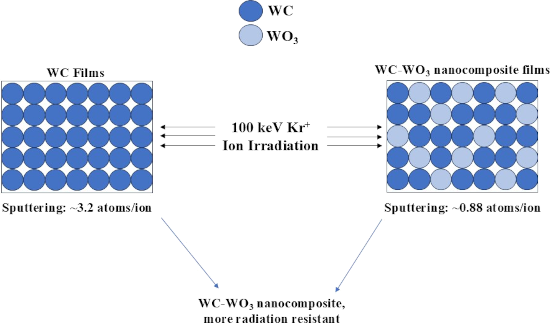
- experimental sputtering trends. Furthermore, preferential sputtering of lower-Z elements (C and O) was observed in both material systems. Glancing incidence X-ray diffraction analysis revealed post-irradiation grain growth in WC–WO3 films, while scanning electron microscopy results show morphological changes
- , Netherlands) in the 2θ range from 20° to 80°. Scanning electron microscopy measurements of pristine and irradiated S1 films were performed using a MIRA Tescan II SEM at a high voltage of 25 kV using detector working in secondary-emission mode. Results and Discussion Phase and compositional studies of the



Supramolecular one-dimensional conducting nanofibers from a C3-symmetric tetrathiafulvalene derivative
Beilstein J. Nanotechnol. 2026, 17, 872–881, doi:10.3762/bjnano.17.63
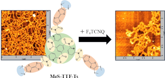
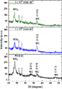
- marked differences in the observed morphologies. In addition to AFM observations, scanning electron microscopy (SEM) measurements were performed for representative samples deposited on HOPG substrates. Representative SEM images are provided in Supporting Information File 1 (Figures S2–S4). The


Glycerol photoelectrochemical oxidation reaction at carbon nitrides/BiVO4 materials
Beilstein J. Nanotechnol. 2026, 17, 806–817, doi:10.3762/bjnano.17.57
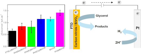
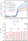
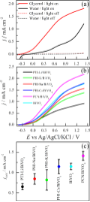
- acetylacetonate at 500 °C for 2 h. The CN/BiVO4 heterojunctions presented bandgap energy values, Eg, similar to pure BiVO4. X-ray diffraction analysis also revealed that the BiVO4 phase was not altered by the presence of the CN. However, scanning electron microscopy analysis coupled to energy-dispersive X-ray
- acquired from 10° to 80° at a rate of 2°·min−1 with a step size of 0.02°. Morphological features and elemental composition were determined by field-emission scanning electron microscopy (FEG-SEM; Zeiss Supra35) coupled with energy-dispersive X-ray spectroscopy (EDS), operating at 15 kV. Optical properties




Tailoring Ag–Pt nanoalloys through solid-state dewetting: structural and optical insights
Beilstein J. Nanotechnol. 2026, 17, 748–759, doi:10.3762/bjnano.17.52

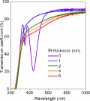
- under an argon atmosphere. The process induced the transformation of continuous bilayers into isolated nanoislands through solid-state dewetting. Scanning electron microscopy and transmission electron microscopy analyses revealed the formation of well-defined, nearly spherical nanoislands with a
- a region with a lower film thickness at grain boundaries, which is well visible on the linear AFM profile in Figure 1 [45][46][47]. Figure 2a presents an exemplary scanning electron microscopy (SEM) image of nanostructures formed as a result of annealing of a silver–platinum bilayer with a thickness




Oxidative atmosphere-driven formation of single-phase spinel CuRh2O4 nanofibers for alkaline water oxidation
Beilstein J. Nanotechnol. 2026, 17, 737–743, doi:10.3762/bjnano.17.50
- characterization Morphology and elemental composition of the synthesized nanomaterials were examined using field-emission scanning electron microscopy (FE-SEM; JEOL JSM-6700F) and high-resolution transmission electron microscopy (HRTEM; JEOL JEM-2100F). Surface chemical states and crystallographic structures were
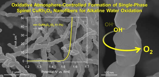
- electron microscopy (SEM) was employed to investigate the surface morphology and structural uniformity of the electrospun nanofibers after post-annealing. In the as-spun state prior to annealing, the fibers containing PVP exhibit smooth surfaces with an average diameter of approximately 300 nm (Supporting
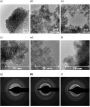
- interplanar spacing of 0.494 nm, corresponding to the (101) plane [19]. Selected area electron diffraction (SAED) patterns display ring-like diffraction features consistent with polycrystalline spinel CuRh2O4, further verifying the formation of the intended crystalline phase. As shown in Figure 5, scanning




Environmental applications of silver nanoparticles: state-of-the-art review and emerging trends
Beilstein J. Nanotechnol. 2026, 17, 697–736, doi:10.3762/bjnano.17.49
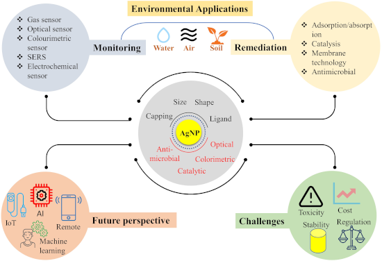
- X-ray analysis [49]. TEM analysis is performed on copper grids with varying mesh sizes and coatings, with carbon/formvar-coated copper grids commonly preferred. Scanning electron microscopy (SEM) provides information on the silver nanoparticles’ surface properties and the aggregation state of dried


Decontamination from water pollutants and pathogens by electrospun nanofibers doped with heavy-atom-free borafluorene-BODIPY photosensitizers
Beilstein J. Nanotechnol. 2026, 17, 668–682, doi:10.3762/bjnano.17.46
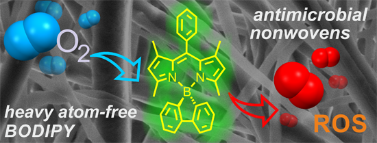
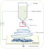
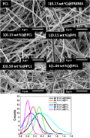
- 30 µm, Rotilabo®, Roth Selection, Germany), which was attached to the collector. After the electrospinning process, all mats were placed under a fume hood for 48 h to evaporate solvents in the fibers. Morphology analysis The morphological properties of samples were examined through scanning electron
- microscopy (SEM) using a JSM-6010PLUS/LV InTouchScope™ system from JEOL (Tokyo, Japan), operating at an accelerating voltage of 11 kV. Prior to imaging, each nonwoven sample underwent a double-coating process with a thin gold layer (2–3 nm). Microstructural analysis was subsequently performed utilizing



Two-step laser synthesis of Ag@TiO2 nanomaterials for the photocatalytic degradation of rhodamine B
Beilstein J. Nanotechnol. 2026, 17, 622–634, doi:10.3762/bjnano.17.43
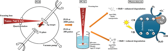
- characterization was performed using scanning electron microscopy (SEM) and transmission electron microscopy (TEM) with energy-dispersive spectroscopy (EDS), aiming to establish a clear correlation between synthesis parameters, nanostructure features, and photocatalytic activity. In our previous studies [6][7][21


Recent progress in enhancing built-in electric fields of perovskite solar cells via junction engineering
Beilstein J. Nanotechnol. 2026, 17, 602–621, doi:10.3762/bjnano.17.42



Eco-efficient materials for agricultural crops based on a mineral rich in MOR- and HEU-type zeolites
Beilstein J. Nanotechnol. 2026, 17, 381–395, doi:10.3762/bjnano.17.26
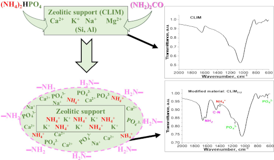
- urea arranged on the surface so that it covers the material and interacts with the zeolitic frameworks, was evidenced by Fourier-transform IR spectroscopy, adsorption measurements, scanning electron microscopy, scanning transmission electron microscopy, and other methods, as well as through culture
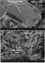
- consequence of the ion exchange processes (Equation 1) occurring during treatment of CLIM with DAP solution, which is in agreement with the data reported in [16][21][42]. Scanning electron microscopy and scanning transmission electron microscopy Microphotography (Figure 5) of natural zeolite (CLIM) revealed
- , the samples were examined by Fourier-transform infrared spectroscopy (FTIR), X-ray diffraction (XRD), scanning electron microscopy (SEM), scanning transmission electron microscopy (STEM), and adsorption measurements based on N2 adsorption isotherms. FTIR spectra were recorded on a Bruker Tensor 27 IR




Interconnection morphology effects on the radio frequency response of carbon nanotube sponges
Beilstein J. Nanotechnol. 2026, 17, 343–351, doi:10.3762/bjnano.17.23
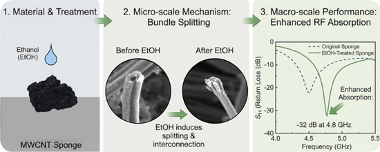
- . In particular, we observed that the response of S11 = −22.6 dB around 4.8 GHz from the CNS antenna improved after a mild treatment with ethanol, reaching S11 = −32.6 dB measured after 10 min of waiting. This observed effect is studied in detail with scanning electron microscopy and Raman spectroscopy
- findings point to a different interpretation related to the morphological effect of ethanol on the CNT mesh [27][29]. A scanning electron microscopy (SEM) study provided insights into the microstructure of the CNT film (Supporting Information File 1, Figure S1) and the sponges (Figure 3). The study



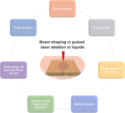
Beam shaping techniques for pulsed laser ablation in liquids: Unlocking tunable control of nanoparticle synthesis in liquids
Beilstein J. Nanotechnol. 2026, 17, 309–342, doi:10.3762/bjnano.17.22







Durable antimicrobial activity of fabrics functionalized with zeolite ion-exchanged nanomaterials against Staphylococcus aureus and Escherichia coli
Beilstein J. Nanotechnol. 2026, 17, 262–274, doi:10.3762/bjnano.17.18
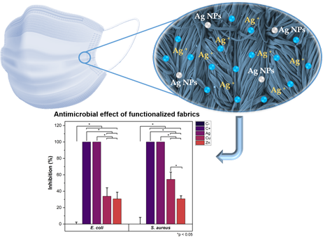
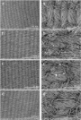
- atom % are evaluated regarding their antimicrobial activity against Staphylococcus aureus (Gram-positive) and Escherichia coli (Gram-negative), as well as regarding their physicochemical and mechanical properties. Scanning electron microscopy confirms the uniform distribution and successful
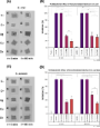
- ). Scanning electron microscopy confirmed the effective incorporation and uniform distribution of the nanomaterials on the fabric surface, facilitated by a 10% w/w acrylic resin binder. Among the tested materials, silver-based fabrics displayed the highest antibacterial efficacy, followed by copper and zinc




Multilayered hyperbolic Au/TiO2 nanostructures for enhancing the nonlinear response around the epsilon-near-zero point
Beilstein J. Nanotechnol. 2026, 17, 251–261, doi:10.3762/bjnano.17.17
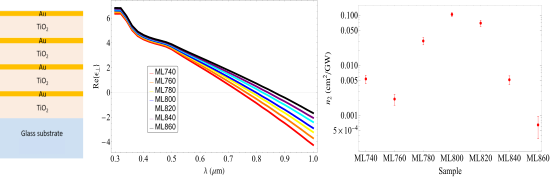
- oscillator as a starting material for Au, and with TiO2 with Cody–Lorentz oscillators as starting material for TiO2. Scanning electron microscopy (Hitachi SU8030) was used to obtain the cross-sectional image (below in Figure 4a), with the sample oriented to expose the ENZ material edge to the electron beam
- the deposited layers. In Table 1, we can see that we have widths for every stack that are different from the ones proposed for the simulated ENZ points. This change in thickness was also seen in scanning electron microscopy (SEM). In Figure 4a we present a SEM image of the ML800 structure; we see that
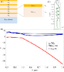
- dm = 10 nm gold layer measured using spectral ellipsometry compared to the one reported in literature. We observe that the resulting permittivity is almost similar to the one used for the simulations. (a) Scanning electron microscopy image of the ML800 structure. We see that the deposited layers have


Comparative study on 3D morphologies of delignified, single tracheids and fibers of five wood species
Beilstein J. Nanotechnol. 2026, 17, 239–250, doi:10.3762/bjnano.17.16
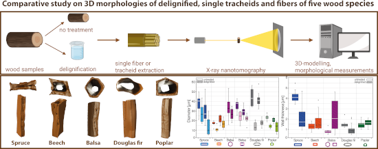
- . Scanning electron microscopy was used to compare the morphology between untreated and delignified fibers and tracheids. X-ray tomography enabled us to reconstruct high-resolution 3D models of delignified single tracheids or fibers, providing information on the pit arrangements. Moreover, delignification
- species in this study by observation of the structural differences after delignification. Using X-ray tomography, we were able to build 3D models of single fibers and tracheids. Additionally, we imaged untreated and delignified samples using scanning electron microscopy for measuring fiber and tracheid
- nitrogen and subsequent lyophilization overnight (−45 °C, 0.080 mbar, Christ Alpha 2–4 LDplus, Christ, Osterode, Germany). Scanning electron microscopy Air-dried wood samples of each of the five species (untreated and delignified) were glued onto metal (SEM) stubs and sputter-coated with a 10 nm layer of


Gold nanoparticle-decorated reduced graphene oxide as a highly effective catalyst for the selective α,β-dehydrogenation of N-alkyl-4-piperidones
Beilstein J. Nanotechnol. 2026, 17, 218–238, doi:10.3762/bjnano.17.15
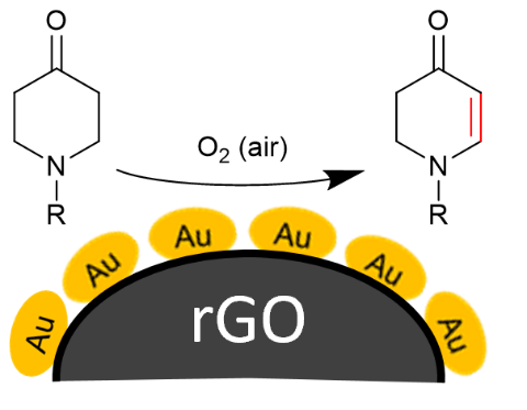
- , scanning electron microscopy (SEM) and nitrogen gas sorption surface area analysis using the Brunauer–Emmett–Teller (BET) theory were employed to evaluate the surface structure, porosity, and overall texture of the materials. The SEM image in Figure 2a reveals the typical structure of AC, characterized by


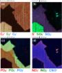
Time of flight secondary ion mass spectrometry imaging of contaminant species in chemical vapour deposited graphene on copper
Beilstein J. Nanotechnol. 2026, 17, 200–213, doi:10.3762/bjnano.17.13
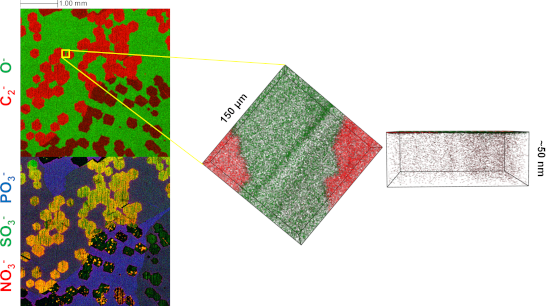
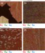
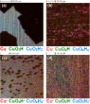
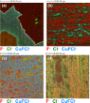
- a Wyko NT1100 White Light Optical Profiling System using a 20× magnification in vertical scanning interferometry (VSI) mode. Scanning electron microscopy (SEM) was carried out with a Carl Zeiss SIGMA VP at an acceleration voltage of 2 kV to ensure sample consistency. Four separate Cu foil samples





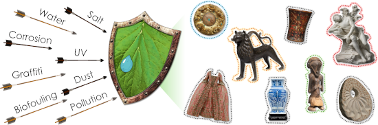
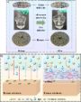
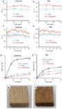
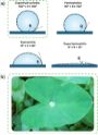
Functional surface engineering for cultural heritage protection: the role of superhydrophobic and superoleophobic coatings – a comprehensive review
Beilstein J. Nanotechnol. 2026, 17, 63–96, doi:10.3762/bjnano.17.6




Subdigital integumentary microstructure in Cyrtodactylus (Squamata: Gekkota): do those lineages with incipiently expressed toepads exclusively exhibit adhesive setae?
Beilstein J. Nanotechnol. 2026, 17, 38–56, doi:10.3762/bjnano.17.4
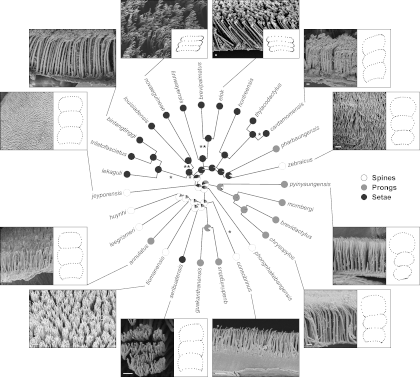
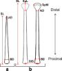
- variation of digital form within this genus, from species with ancestrally small, round subdigital scales to macroscopically defined incipient toepads (broadened lamella-like subdigital scales). We employed scanning electron microscopy (SEM) and phylogenetic comparative methods to (a) explore the


Reduced graphene oxide paper electrode for lithium-ion cells – towards optimized thermal reduction
Beilstein J. Nanotechnol. 2026, 17, 24–37, doi:10.3762/bjnano.17.3
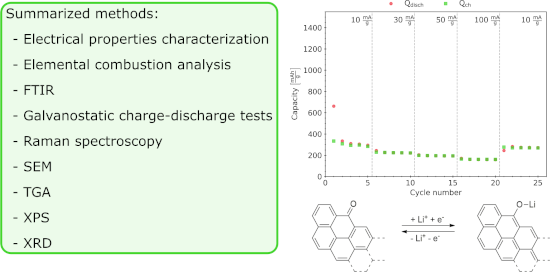
- and thickness were determined with scanning electron microscopy imaging. This paper also reveals electrical and electrochemical properties of the material. The conductivity of the material obtained at 800 °C reached ≈70 S/cm, and the discharge capacity reached ≈160 mAh/g at 100 mA/g current density