Search results
Search for "substrate" in Full Text gives 1262 result(s) in Beilstein Journal of Nanotechnology. Showing first 200.
Carbon nanotube-cellulose ink for rapid solvent identification
Beilstein J. Nanotechnol. 2023, 14, 535–543, doi:10.3762/bjnano.14.44

- [39][40]. Besides, graphene films deposited on cellulose paper and a graphene/cellulose composite were also reported as a solvent sensor material [30][33]. However, most of these works rely on cellulose as a paper substrate or as a thick composite film that cannot be readily employed for large-scale
- more information). Also, to compare our results with a simple conductive response to the pure liquids, we performed control experiments on a substrate without applying the ink. Our sensor film proved to be two orders of magnitude more sensitive than the bare substrates with only electrical contacts


Nanoarchitectonics to entrap living cells in silica-based systems: encapsulations with yolk–shell and sepiolite nanomaterials
Beilstein J. Nanotechnol. 2023, 14, 522–534, doi:10.3762/bjnano.14.43

- conditions had been determined, the preparation of the G57-4 silica gel substrate was used to produce diverse biohybrid systems incorporating living cyanobacterial or yeast cells, as well as pre-synthesised yolk–shell bionanobybrids. In all cases, the microstructural features of the resulting biohybrid
- morphology. This image focusses on a “hollow region” of yeast cells encapsulated into the silica gel substrate. In Figure 2B, pseudohyphal growth is clearly observed, yielding long filaments of associated cells that expand as a three-dimensional network within the matrix. In this hollow region within the
- improved transport of nutrients and metabolites across the material. The FE-SEM images in Figure 2C and Figure 2D show the same microorganism cells but previously encapsulated in yolk–shell microstructures. They are arranged differently from those immobilized freely in the silica gel substrate. In the


Microneedle patches – the future of drug delivery and vaccination?
Beilstein J. Nanotechnol. 2023, 14, 494–495, doi:10.3762/bjnano.14.40

- diagnostics. Microneedles provide shallow transdermal access to the ISF and are an excellent match to these and other developments when integrated into arrays on a substrate to form a patch. The possibility of inexpensive mass-manufactured MN patches for drug delivery, vaccination, and diagnostic testing is a
A mid-infrared focusing grating coupler with a single circular arc element based on germanium on silicon
Beilstein J. Nanotechnol. 2023, 14, 478–484, doi:10.3762/bjnano.14.38

- cover the wavelength of 6–15 μm. Hence, it is a suitable material for biosensors applications in the MIR band [6]. In recent years, researchers have verified the feasibility of Ge MIR waveguides on various substrate materials, such as germanium on silicon (Ge-on-Si), germanium on silicon-on-insulator
- (GOSI) [7], germanium on insulating substrate (GOI) [8][9], and germanium on silicon nitride substrate (GOSN) [10]. Among them, Ge-on-Si platforms have been widely applied in on-chip sensors, nonlinear optics, free space communication, and thermal imaging [1][6] because portable, cost-effective, and
- waveguide with a focusing subwavelength grating MIR grating coupler, the difficulty of preparation has been considerably reduced. Principle and Design Figure 1a shows the tilted view of the proposed MIR FGC. The Ge waveguide layer is built onto the Si substrate forming the Ge-on-Si structure. The proposed


Conjugated photothermal materials and structure design for solar steam generation
Beilstein J. Nanotechnol. 2023, 14, 454–466, doi:10.3762/bjnano.14.36

- formed by sequential polymerization on paper substrates, to enhance their light capturing capability (Figure 6a) [32]. Transmission and diffuse reflectance measurements of the PPy nanosheets confirmed that the multilayer PPy nanosheets on the paper substrate exhibited a distinct broadband absorption in
- process of multilayer PPy nanosheets. (b)Transmittance and (c) diffuse reflectance spectra of the air-laid paper substrate coated with different layer numbers of PPy nanosheets. The inset figure in (b) is the enlarged view of the 500–1500 nm wavelength range. The solar spectral irradiance (AM1.5G) is


Molecular nanoarchitectonics: unification of nanotechnology and molecular/materials science
Beilstein J. Nanotechnol. 2023, 14, 434–453, doi:10.3762/bjnano.14.35

- solid substrate could be a key technology for building nanoscale electronic circuits. Nakayama and co-workers have succeeded in controlling the self-assembly and intermolecular chemical reactions of functional molecular components predeposited on a solid surface [112]. Specifically, they fabricated
- molecule–polymer nanoconjugates consisting of C60 molecules and polydiacetylene nanowires at designated locations on a solid surface (Figure 2). First, diacetylene monomers were self-assembled on the solid substrate. Then, polydiacetylene nanowires were formed by chain polymerization between the monomer
- multistep electrochemical epitaxial polymerization technique [113]. This technique consists of combining two electrochemical polymerization processes using different monomer solutions. First, a voltage pulse was applied to an iodine-covered Au(111) substrate in an electrolyte solution containing the first


Evaluation of electrosynthesized reduced graphene oxide–Ni/Fe/Co-based (oxy)hydroxide catalysts towards the oxygen evolution reaction
Beilstein J. Nanotechnol. 2023, 14, 420–433, doi:10.3762/bjnano.14.34
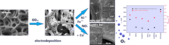
- CoNiFe-GO were fabricated without any additives directly on the nickel foam substrate. A significant improvement of the OER activity was observed after combining NiFe with GO (OER overpotential η(10 mA·cm−2): 210 mV) compared to NiFe (η: 235 mV) and GO (η: 320 mV) alone. A different OER activity was
- electrode can also be improved by choosing a conductive and/or high surface area substrate, such as porous nickel foam [22][23]. In the literature, some research has been performed to evaluate the OER electrocatalytic performance of hybrid materials of Ni-, Fe- and/or Co-based oxides/(oxy)hydroxides and Gr
- the surface of nickel foam. The chronoamperometric graph recorded during the deposition is presented in Figure 1a. Each synthesis (except that of GO) began with a fast increase of the cathodic current, which is associated with the formation of the new catalyst phase on the surface of the substrate [25


Plasmonic nanotechnology for photothermal applications – an evaluation
Beilstein J. Nanotechnol. 2023, 14, 380–419, doi:10.3762/bjnano.14.33

- nanoparticles induces dipoles in the substrate atoms in proximity of this polarization field, which in turn affects the nanoparticle resonance. This has been observed to induce higher-order resonances when the mismatch between the permittivity of the substrate and the surrounding of the nanoparticle increases
- , as well as to (depending on the orientation of the applied field with respect to the induced fields in the nanoparticle and the substrate) increase or decrease in the absorption intensity [49][50][51]. It follows from the discussion that considerable effects to the plasmon resonance are affected by


The steep road to nonviral nanomedicines: Frequent challenges and culprits in designing nanoparticles for gene therapy
Beilstein J. Nanotechnol. 2023, 14, 351–361, doi:10.3762/bjnano.14.30

- approach is that accounting for substrate contributions or proving the full availability of the NAT can be difficult and laborious. Alternatively, chromatographic and size-exclusion techniques, elemental analysis, or polymerase chain reaction (PCR) [60] mass spectrometry [61] can be effective if the
- E2859-11 for AFM analysis, and ISO 21363:2020 for substrate-supported TEM analysis. When at all possible, obtaining the distribution of sizes from these methods with extension to obtain geometric properties (aspect ratio, minimum diameter, circularity, roundness, or sphericity) will allow for the
- destruction of valuable media to fundamental changes to the payload. While several multimethod approaches may be capable of providing the ratio between mass of payload and mass of substrate, the mass of payload per unit volume, and the number of payload molecules per particle, there is no single commercial


Quasi-guided modes resulting from the band folding effect in a photonic crystal slab for enhanced interactions of matters with free-space radiations
Beilstein J. Nanotechnol. 2023, 14, 322–328, doi:10.3762/bjnano.14.27

- index 1.45) substrate as an example to demonstrate that these modes can be switched to QGMs with ultrahigh Q-factors over a large operating bandwidth, as shown in Figure 1. When all air holes have the same radius, the whole structure represents a two-dimensional PCS structure with a square primitive


Bismuth-based nanostructured photocatalysts for the remediation of antibiotics and organic dyes
Beilstein J. Nanotechnol. 2023, 14, 291–321, doi:10.3762/bjnano.14.26

- semiconductor as well as the redox levels of the substrate [11][21]. One of the main barriers preventing photocatalysis from being used in practical applications is the lack of suitable semiconductor photocatalysts. The commonly used nanometre-sized photocatalysts are metal oxides or sulfides (binary compounds


Biocatalytic synthesis and ordered self-assembly of silica nanoparticles via a silica-binding peptide
Beilstein J. Nanotechnol. 2023, 14, 280–290, doi:10.3762/bjnano.14.25

- combination with NH3. The reaction kinetics were monitored via measuring the optical density (OD) with UV–vis spectroscopy and the conversion of substrate via gas chromatography coupled with mass spectroscopy (GC–MS). Size and net surface charge distribution of the particles were determined with dynamic light


Recent progress in cancer cell membrane-based nanoparticles for biomedical applications
Beilstein J. Nanotechnol. 2023, 14, 262–279, doi:10.3762/bjnano.14.24

- incorporated surface-modified PD-L1 inhibitory peptide and MMP2 substrate peptide [54]. Manganese oxide (MnO2)-based NPs function as MRI imaging agents and can also utilize Fenton-like reactions to deplete GSH and generate •OH to mediate tumor cell death [123]. In the work of Fu et al., a hollow MnO2 NP-based


A novel approach to pulsed laser deposition of platinum catalyst on carbon particles for use in polymer electrolyte membrane fuel cells
Beilstein J. Nanotechnol. 2023, 14, 190–204, doi:10.3762/bjnano.14.19

- carbon substrate and the chemical synthesis of PtNPs during catalyst fabrication. Platinum was deposited on carbon particles at room temperature using a pulsed laser deposition (PLD) system equipped with an ArF excimer laser (λ = 193 nm). The uniform deposition of PtNPs on carbon supports was achieved
- from the platinum target to eliminate the chemical functionalization of the carbon substrate and the chemical synthesis of PtNPs. The Pt catalyst was deposited on synthesized highly graphitized carbon particles and XC-72R commercial carbon support using PLD with a specially designed electromechanical


High–low Kelvin probe force spectroscopy for measuring the interface state density
Beilstein J. Nanotechnol. 2023, 14, 175–189, doi:10.3762/bjnano.14.18

- interface state density in the semiconductor bandgap. We also demonstrate using a pn-patterned silicon substrate that the interface state density can be measured. Theory To understand the principle of the high–low KPFS proposed in this study, we discuss the electrostatic forces acting between the tip and
- (Figure 1a). No oxide film on the semiconductor surface is assumed, and to simplify the discussion, the CPD between the tip and the semiconductor substrate is assumed to be zero. To investigate the electrostatic force acting between the tip and the semiconductor surface, we use the theoretical model
- potential), the lifetime has been reported to be less than 5 × 10⁻⁶ s. These results indicate that the cutoff frequency fc of carrier transport between the interface and bulk states for a Si substrate with a low carrier density is approximately 200 kHz. Therefore, when an AC bias voltage with a frequency


Formation of nanoflowers: Au and Ni silicide cores surrounded by SiOx branches
Beilstein J. Nanotechnol. 2023, 14, 133–140, doi:10.3762/bjnano.14.14

- substrate at higher temperatures in oxygen-deficient environment [3][4]. Another cost-effective nanofabrication method, thin film dewetting, driven by the reduction of the surface energy and the interface energy has also been profusely studied because it provides a straightforward and fast way to produce
- forming gas (mixture of Ar and H2), scattered spots (Supporting Information File 1, Figure S1) can be found on the surface. The enlarged insets present the circular feature of those spots and their height distributions indicate that circular areas are below the substrate surface. Hence, they will be
- (Supporting Information File 1, Figure S2). A similar concentration of O and Si corresponding to the substrate agrees well with Figure 1e. However, a much higher O concentration than that of Si corresponding to the branch part proves the possibility of SiOx branches again. Also, both Au and Ni show negligible


Characterisation of a micrometer-scale active plasmonic element by means of complementary computational and experimental methods
Beilstein J. Nanotechnol. 2023, 14, 110–122, doi:10.3762/bjnano.14.12

- on a sapphire substrate via physical vapour deposition (PVD). After this, two separate AFMs are used to machine channels in the silver film to create the desired constriction, which in this case measures 10 μm. The tip of the AFM is held at a set loading force in contact with the thin metal film and
- deposition substrate for a thin silver film of 48 nm. The incident angles were referenced to the air–prism interface. The sinusoidal current was generated using a function generator with a current buffer to ensure impedance matching to the system under investigation. A transimpedance-amplified photodiode
- the scan. The substrate used to generate the SPR response is sapphire with a refractive index of n = 1.7717 at λ = 561 nm. SJEM experiment To further characterise the active plasmonic element, in complement with the SPR curve measurements above, the thermal distribution due to Joule heating of the


Antimicrobial and mechanical properties of functionalized textile by nanoarchitectured photoinduced Ag@polymer coating
Beilstein J. Nanotechnol. 2023, 14, 95–109, doi:10.3762/bjnano.14.11

- ] synthesized AgNPs on cotton fabrics using laser ablation, while Ahmad et al. [31] deposited AgNPs by the dip and dry method based on surface reduction reactions. However, the difference in expansion coefficients of the given metal layer and substrate can lead to surface defects under strain (cracks, loss of
- [41]. The polymer coating adapts to various textile shapes, improves the adhesion between the MNPs and the substrate by compensating internal stresses and maintains the antimicrobial properties of the NPs. As the nanoparticles are embedded inside the polymer matrix, they are protected from external
- been carried out on the coating of unaltered textile substrates with hybrid MNP-polymer films for antimicrobial applications. In a previous work [47][48], we presented an innovative one-pot, one-step photoinduced synthesis to generate silver and gold-polymer nanofilms on a glass substrate. The kinetic


Combining physical vapor deposition structuration with dealloying for the creation of a highly efficient SERS platform
Beilstein J. Nanotechnol. 2023, 14, 83–94, doi:10.3762/bjnano.14.10

- resulting signal intensity tends to strongly vary due to surface contamination [30]. In this paper, a simple synthesis method to design bimodal porous silver substrate for SERS is reported. Magnetron co-sputtering of a silver and aluminum target was used for the deposition of the precursor alloy thin film
- growth of Ag–Al crystallites in a truncated octahedron shape at low temperatures (below 170 °C) [32][33]. Due to the rather short distance between the substrate and the target (i.e., 10 cm), particles have greater mobility, resulting in the growth of crystalline structures [34]. This induces the faceting
- of the crystallite and promotes growth in a hexagonal shape. The dispersed column structure can be the consequence of the hexagonal growth and substrate rotation during deposition. Due to the specific geometry of our setup (i.e., the angle between the normal of the substrate and the targets is 30


Liquid phase exfoliation of talc: effect of the medium on flake size and shape
Beilstein J. Nanotechnol. 2023, 14, 68–78, doi:10.3762/bjnano.14.8

- substrate appears in black to dark blue. Following previous works, we consider flakes with ten or less layers as “few-layer” [25]. Since talc has a layer thickness of approximately 1 nm [12], we did not convert the height to the number of layers as it is a direct conversion. Few-layer flakes appear in light
- et al. [24] and Santos and co-workers [25]. In short, a solution (1:40) of APTES in DI water was prepared. Si/SiOx substrates were immersed in the solution for 15 min. Subsequently, each substrate was rinsed with DI water and blown dry with pure N2 five times to ensure the removal of any residual
- APTES molecules. This step is crucial to ensure that talc flakes of all sizes adhere to the substrate and do not stack. Talc deposition is achieved employing spread coating of the solution onto the functionalized substrate. A drop that covers all the substrate is deposited on the surface and allowed to


Gap-directed chemical lift-off lithographic nanoarchitectonics for arbitrary sub-micrometer patterning
Beilstein J. Nanotechnol. 2023, 14, 34–44, doi:10.3762/bjnano.14.4

- modulating stamp properties for micrometer-scale features [27]. utilizing different assembled and backfilled species [28][29]. and further substrate processing, e.g., pattern transfer to the underlying material layer [30][31][32][33][34][35][36]. In practice, CLL allows simple and facile fabrication of
- stamp and the substrate, and are viewed as nuisances that hinder technique resolution and reproducibility [37][38][39][40][41][42]. Careful treatments on stamp feature design and aspect ratio tuning are therefore necessary to achieve desirable patterning results. Although this problematic issue may
- cause lithographic limitation, the structural gaps generated at the stamp–substrate interface during the contacting stage can provide another opportunity to create minute geometries. For example, nanochannels with height on the order of 10 nm and millimeters in length can be created when a nanowire is


The influence of structure and local structural defects on the magnetic properties of cobalt nanofilms
Beilstein J. Nanotechnol. 2023, 14, 23–33, doi:10.3762/bjnano.14.3

- that are influenced and corrected in the manufacturing process). The previously conducted studies considered the influence of sample parameters (e.g., temperature of the substrate on which the magnetron sputtering of nanofilms takes place, the intensity and deposition direction) on the final properties
- additional processing means, such as mechanical alignment and intensive substrate cooling. The stage of experimental studies of the sample structure is necessary to identify the real structure of the nanocomposite and to compare the data with previously obtained simulation results. This current work is aimed
- horizontal layers, is shown in Figure 2. The legend to the figure provides information about the temperature of the substrate on which nanofilms were deposited in the numerical experiments. Niobium is known as one of the most actively used superconductors [46][47] with a superconducting transition


Electrical and optical enhancement of ITO/Mo bilayer thin films via laser annealing
Beilstein J. Nanotechnol. 2022, 13, 1589–1595, doi:10.3762/bjnano.13.133

- adherence to the substrate, very high thermal stability (up to 600 °C), and high electrical conductivity [14]. Over the last decades, the development of solar cells has grown dramatically. The cells have become larger, thinner, and lighter. This increases the electrical resistivity, which is undesirable
- by many factors, such as the type of substrate [15], the deposition technique [16][17][18], the deposition conditions [19][20][21][22], and the annealing treatment [23]. Among these factors, heat treatment is a significant factor in rearranging the nanostructure, removing defects, and improving the


Observation of collective excitation of surface plasmon resonances in large Josephson junction arrays
Beilstein J. Nanotechnol. 2022, 13, 1578–1588, doi:10.3762/bjnano.13.132

- formation of standing waves at the electrode/substrate interface. We observe that resonant steps in the current–voltage characteristics appear above some threshold number of junctions, Nth ≈ 100, and then progressively enhance in amplitude with further increment of the number of junctions in the resistive
- profound step structure in the current–voltage (I–V) characteristics. The resonances are caused by the formation of surface plasmon-type standing waves at the electrode–substrate interface [34]. Thus, the electrodes themselves act as a common external resonator, facilitating the effective indirect coupling
- interconnecting Nb electrodes, acting as a travelling wave antenna for surface plasmons at the electrode–substrate interface [9][34]. The linear array contains also two extra Nb lines (without JJs) on each side of the array forming a slot waveguide, which may act as an additional external resonator. However


Utilizing the surface potential of a solid electrolyte region as the potential reference in Kelvin probe force microscopy
Beilstein J. Nanotechnol. 2022, 13, 1558–1563, doi:10.3762/bjnano.13.129

- electrode placed on a solid electrolyte (Li-ion conductor) substrate. The surface-potential distribution in the region across the solid electrolyte was measured with a DC voltage applied between the Au electrodes. During the KPFM measurements, the potential of each Au electrodes relative to the Li electrode
- electrochemical cell, where two Au electrodes and one metallic Li reference electrode were placed on the solid electrolyte substrate. The changes in the surface potential of the Au electrodes, measured relative to the surface potential of the solid electrolyte region, agreed well with the changes in the Au
- electrolyte sample was a Li-ion conducting glass ceramic purchased from OHARA Inc. (LICGCTM AG-01) [20]. The size and thickness of the substrate were 25.4 mm × 25.4 mm and 150 μm, respectively. The main crystalline phase was Li1+x+yAlx(Ti,Ge)2−xSiyP3−yO12 [20]. The substrate was cut into pieces of


