Abstract
Thinning out MoS2 crystals to atomically thin layers results in the transition from an indirect to a direct bandgap material. This makes single layer MoS2 an exciting new material for electronic devices. In MoS2 devices it has been observed that the choice of materials, in particular for contact and gate, is crucial for their performance. This makes it very important to study the interaction between ultrathin MoS2 layers and materials employed in electronic devices in order to optimize their performance. In this work we used NC-AFM in combination with quantitative KPFM to study the influence of the substrate material and the processing on single layer MoS2 during device fabrication. We find a strong influence of contaminations caused by the processing on the surface potential of MoS2. It is shown that the charge transfer from the substrate is able to change the work function of MoS2 by about 40 meV. Our findings suggest two things. First, the necessity to properly clean devices after processing as contaminations have a great impact on the surface potential. Second, that by choosing appropriate materials the work function can be modified to reduce contact resistance.
Introduction
Due to their unique properties which can differ a lot compared to bulk materials, two-dimensional materials are being targeted in a variety of research areas like surface physics, electrical engineering, chemistry and biomedical applications [1-4]. The 2D-material getting the most attention besides graphene are single layers of molybdenum disulfide (SLM) which consist of a plane of molybdenum atoms that are sandwiched between sulfur atoms. The main reason for this is the transition from an indirect (bulk MoS2) to a direct (single layer MoS2) band gap semi-conductor [5]. Single layer MoS2 has a strong photoluminescence signal [5-9] and other interesting properties like a mechanical stiffness of 180 ± 60 N·m−1, which is comparable to steel [10,11], charge carrier mobilities that are comparable to Si [12,13], and it is possible to grow these ultrathin layers using CVD [14-16]. The main advantage SLM has to offer compared to the model 2D-material graphene is its direct band gap. It allows the facile integration of SLM in electronic devices, which has been demonstrated for highly flexible transistors, optoelectronic devices, small-signal amplifiers, MoS2 integrated circuits and chemical vapor sensors [12,17-21]. It has been reported that the performance of these devices can greatly vary due to the choice of the material of the contacts, the cleanliness of the SLM surface and a top gated structure with a high κ dielectric [22-27]. By choosing appropriate materials in 2D-devices the work function can be tuned to, e.g., lower the contact resistance and improve their performance. First experiments adressing this issue for MoS2 by using Kelvin probe force microscopy (KPFM) have already been reported [28,29]. However, these measurements were not done on SLM but bilayer MoS2 (BLM) and higher layer numbers and the measurements were performed under ambient conditions using amplitude modulated KPFM, both having a great impact on the results. In this work we study the work function of SLM on a standard SiO2/Si substrate using non-contact atomic force microscopy (NC-AFM) and Kelvin probe force microscopy in situ. In our measurements we use a gold contact patterned on SLM in order to calibrate the work function of our AFM tip which allows us to determine quantitative work function values for SLM, BLM and few layer MoS2 (FLM). Additionaly, we use reactive ion etching to pattern holes into the SiO2 substrate. By comparing the work function of SLM on etched and pristine SiO2 substrates, we show that a significant change in the work function can be achieved by substrate effects.
Experimental
For our studies we exfoliated MoS2 (HQgraphene, Netherlands) on a patterned Si sample that has been covered by 90 nm SiO2 layer (graphene supermarket, Calverton, NY, USA). The SiO2 was patterned by using an inductive coupled plasma reactive ion etching (ICP-RIE) with Cl2/N2 chemistry. The etching mask used was a standard photoresist patterned by optical lithography. The etching was performed at 35 °C using 300 W of ICP and 150 W table power. The chamber pressure was adjusted to 8·10−3 mbar during this procedure. Reactive ion etching was employed to locally alter the surface roughness and introduce defects in the SiO2 substrate [30,31]. The resulting structures on the SiO2 surface consist of etched holes with a depth of about 40 nm measured using AFM. Immediately after etching, the MoS2 was exfoliated by mechanical cleavage [32]. Single layer MoS2 flakes were located by using their optical contrast and verified using Raman spectroscopy [33,34]. For Raman point measurements and mappings, a Renishaw InVia Raman spectrometer (λ = 532 nm, P < 0.4 mW, spectral resolution ≈ 1 cm−1) has been employed. Because SLM is highly flexibel, it is not covering the etched hole. Instead the SLM touches the etched SiO2 surface at the bottom and follows the morphology like a membrane (Figure 1). While this leaves the SLM heavily strained on the edge of the hole, it allows to experimentally compare the effect of two differently treated subtrates (SiO2 and RIE SiO2) on the same MoS2 flake. After identification of SLM areas, a Ti/Au (5 nm/15 nm) contact was patterned on the MoS2 flake by photolithography. We used the Photoresist ARP-5350 (Allresist GmbH, Strausberg, Germany) with the developer AR 300-35 (Allresist GmbH, Strausberg, Germany). Acetone was used for the lift-off and finally the samples were boiled in isopropyl alcohole. The contact served two purposes. On the one hand, the sample was electrically connected to ground potential, on the other hand, the gold surface was used for calibrating the work function of the AFM tip during KPFM measurements.
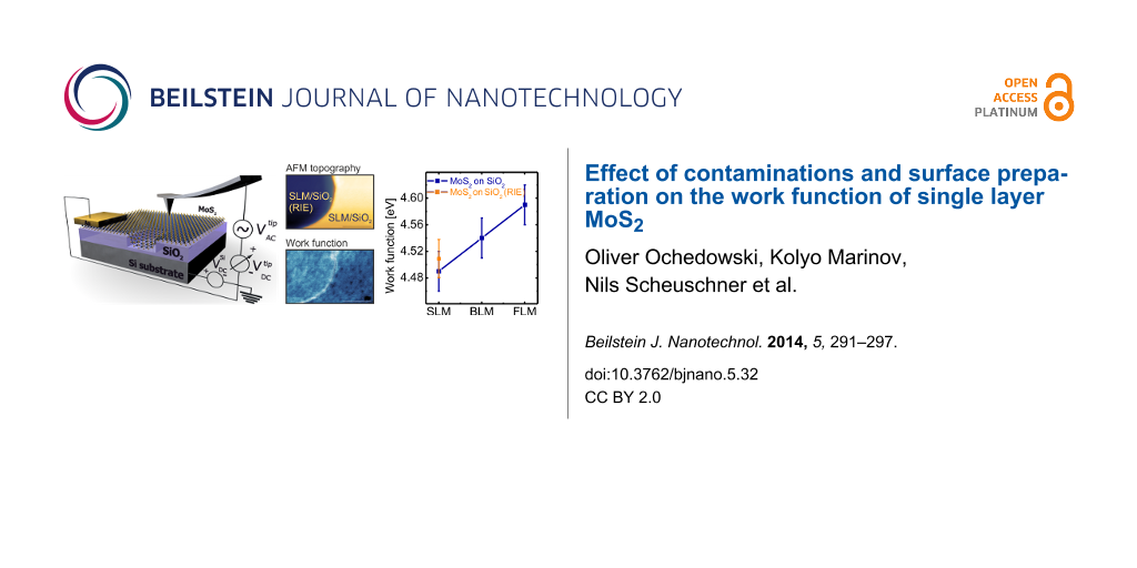
![[2190-4286-5-32-1]](/bjnano/content/figures/2190-4286-5-32-1.png?scale=2.0&max-width=1024&background=FFFFFF)
Figure 1: Schematic representation of the KPFM setup and the MoS2 sample with the RIE SiO2.
Figure 1: Schematic representation of the KPFM setup and the MoS2 sample with the RIE SiO2.
The contacted SLM sample is introduced into an ultra high vacuum system with a base pressure of about 2·10−10 mbar. Non-contact AFM measurements were performed using a RHK UHV 7500 system with the PLL Pro 2 controller. Simultaneously to NC-AFM, frequency-modulated KPFM measurements were conducted to probe the local contact potential difference (CPD) between the tip and the surface [35-41]. As force sensors, highly conductive Si cantilevers with a typical resonance frequency of f = 300 kHz (Vistaprobe T300) were utilized. During KPFM measurements an AC voltage is applied to the tip (UAC = 1 V and fAC = 1 kHz) and the built in lock-in amplifier of the PLL Pro 2 is used to apply a DC voltage which minimizes the resulting electrostatic forces between tip and sample surface. This DC voltage corresponds to the local CPD.
Results and Discussion
Raman spectroscopy characterization
In Figure 2 we present an optical image of a sample prepared by the procedure described above together with additional Raman spectroscopy data. The SLM flake can be identified in the optical image in Figure 2a by its contrast, which is a transparent green tone. While the majority of the SLM flake is located on pristine SiO2, a small part of the SLM flake is at the bottom of a hole which was patterned by RIE. To unambiguously identify SLM we used Raman spectroscopy and compared the results to data obtained by literature [34]. In Figure 2b the Raman spectra of SLM on SiO2 and on SiO2 (RIE) as well as FLM on SiO2 is shown. The two prominent peaks, the E2g and A1g peak, correspond to the opposite vibration of the two S atoms with respect to the Mo atom and the out-of-plane vibration of only S atoms in opposite directions, respectively [42,43]. For SLM on SiO2 the Raman shifts obtained for the E2g, ν = 386.1 cm−1, and A1g, ν = 403.0 cm−1, are consistent with values reported by other groups. For higher layer numbers the E2g has been reported to shift to lower wave numbers while the A1g shifts to larger wave numbers which is again in good agreement with our data. However, the SLM on RIE SiO2 shows a different behaviour compared to SLM on pristine SiO2. The E2g is slightly downshifted to ν = 385.2 cm−1 and the A1g shows a minor shift to ν = 403.4 cm−1. Shifts of the E2g and A1g modes of SLM can have multiple reasons. Uniaxial tensial strain has been observed to cause a splitting in the E2g mode and a shift to lower wave numbers for the resulting E− and E+ modes by 4.5 and 1 cm−1/% [44,45]. While the A1g mode shows no distinct sensitivity to uniaxial strain, a charge carrier dependency has been observed [46]. Electron doping of 1.8·1013 cm−2 leads to a linewidth broadening of 6 cm−1 and the phonon frequency decreases by 4 cm−1. As our data shows a shift in both Raman active modes we suggest that the RIE SiO2 surface causes a slight strain and maybe local doping by charge transfer in the MoS2 flake. The Raman mapping shown in Figure 2c corresponds to the evaluation of point spectra performed in the green box marked in Figure 2a. Plotted is the difference of the E2g an A1g mode positions. While the difference between SLM and FLM on SiO2 is significant with Δ = 8.2 cm−1, the difference between SLM on SiO2 and on RIE SiO2 is relatively small with Δ = 1.3 cm−1. As can be seen in the Raman mapping, the difference in the SLM induced by the substrate is constant over the whole flake and not just present in single point meaurements.
![[2190-4286-5-32-2]](/bjnano/content/figures/2190-4286-5-32-2.png?scale=2.0&max-width=1024&background=FFFFFF)
Figure 2: (a) Optical microscope image of an exfoliated MoS2 flake on a prepatterned (RIE) SiO2 substrate. A gold contact was attached to the MoS2 in order to ground the flake for KPFM measurements. (b) Raman spectroscopy spectra of SL and FL MoS2 on SiO2 and SL MoS2 on RIE SiO2. For higher layer numbers the E2g is shifted to lower wave number while the A1g mode is shifted to higher wave numbers. (c) Raman mapping data of the area marked in (a) with the blue box. The difference between A1g and E2g mode is plotted revealing a shift of the Raman modes for SLM on the RIE SiO2 substrate.
Figure 2: (a) Optical microscope image of an exfoliated MoS2 flake on a prepatterned (RIE) SiO2 substrate. A ...
In-situ KPFM on single layers of MoS2
For the NC-AFM and KPFM measurements the sample was introduced to the UHV system. Before the data collection the sample was heated in situ to 200 °C for 30 min to remove any adsorbates from ambience. In Figure 3a and Figure 3c the NC-AFM topography and the corresponding surface potential map are shown, respectively. On the right side the Ti/Au contact can be seen which is about 20 nm high and shows a distinct contrast in the surface potential in comparison to the MoS2 layers. In Figure 3d a surface potential histogram of SLM, FLM and the gold surface of the Ti/Au contact is given. We find a surface potential of 4.27 V for SLM, 4.37 V for FLM and 4.89 V for gold. The surface potential itself is always a relative value based on the local CPD between the AFM tip and the sample surface. To obtain quantitative work function values, we calibrated the tip on the gold surface by using the known work function of gold ΦAu = 5.10 eV [47,48]. With the relation Φ = 5.10eV − e·(CPDAu − CPDnMoS2) the work function of SLM ΦSLM = 4.49 ± 0.03 eV and FLM ΦFLM = 4.59 ± 0.03 eV can be assigned. The given errorbar consists of the experimental error of our system. Not included in this error is band bending, which occurs when doing KPFM measurements on a semi-conductor surface and a false estimation of the work function of the patterned gold contact. Besides graphite [49], gold is a common material to calibrate the work function of the AFM tip [48], but while the work function ΦAu = 5.10 eV is often used, other work function values in the range from 4.74 eV to 5.54 eV have been reported as well [50,51]. Surface roughness, homogeneity and humidity can have an effect on the measured work function of metal surfaces as Guo et al. recently demonstrated [52]. The presented data is measured in situ after annealing and we are therefore confident that humidity can be neglected. We want to point out that an error in the work function calibration does not affect the work function values of SLM, BLM and FLM with respect to each other. While the surface potential on the Au contact in Figure 3 appears uniform, strong local variations can be observed on the MoS2 flake. We attribute these features, marked in Figure 3a with green circles, to contaminations due to the patterning process. The height of these contaminations varies between 1 nm and 20 nm. These contaminations have a noticeable effect on the work function of SLM, as ΦSLM can be lowered by up to 0.15 eV. As the work function of these contaminations is clearly different than that of the Au contact, the contaminations are most likely resist residues which have not been completely removed. Such contaminations may act as scattering centers or charge puddles which are likely to be detrimental to the performance of SLM devices [53]. For graphene and MoS2 it has been shown, that adsorbates due to ambient exposure can have a strong impact on the work function of these materials, like inducing an additional charge transfer or even redox reactions with water [29,54].
![[2190-4286-5-32-3]](/bjnano/content/figures/2190-4286-5-32-3.png?scale=2.0&max-width=1024&background=FFFFFF)
Figure 3: (a) NC-AFM image of MoS2 flake on SiO2 with a gold contact (height = 20 nm). Topography shows areas with contaminations due to processing. (b) Corresponding surface potential image to (a). The surface potential of MoS2 is increasing with increasing layer thickness, contaminations can be clearly distinguished in the surface potential image. (c) Surface potential histogram of the box marked in (b).
Figure 3: (a) NC-AFM image of MoS2 flake on SiO2 with a gold contact (height = 20 nm). Topography shows areas...
In situ screening length of MoS2
In the next step, we determine the work function of BLM and the screening length of MoS2. For this the SLM/BLM/FLM section of Figure 3 has been measured again in more detail and the work function is analyzed by line profiles. Shown in Figure 4a–c are the NC-AFM topography, work function map and the corresponding line profiles, respectively. The measured height for BLM is 0.92 ± 0.10 nm, which is slightly higher than the interlayer spacing of a bulk MoS2 crystal [55]. For FLM we get two different heights, one is 2.96 nm (≈5 layers) and 7.89 nm (≈12–13 layers). In the work function map in Figure 4b, three contrasts can be observed – SLM, BLM and FLM. As the work function for FLM 2.96 nm and the other FLM with 7.89 nm is not changing, we conclude from our data that the screening length of MoS2 is at least 2.96 nm, which is in good agreement with previous findings for annealed MoS2 [29]. Li et al. compared the screening length of pristine MoS2 flakes on SiO2 with annealed MoS2 flakes and found a decrease from approximately 5 nm down to 2.5 nm for annealed MoS2. Our measurements here yield a screening length between 1.6 and 2.96 nm, which is much lower than the value for pristine MoS2. We therefore conclude that the investigated MoS2 is not affected by ambient adsorbates. In Figure 4c we used the line profile to quantify the work function of SLM and BLM. The work function of SLM is determined to be the same as using the histogram analysis in Figure 3 with ΦSLM = 4.49 ± 0.03 eV. The work function of BLM is increased with respect to SLM by about 0.05 eV to ΦBLM = 4.54 ± 0.03 eV. Again, contaminations on BLM appear to decrease the work function as can be seen in Figure 4b.
![[2190-4286-5-32-4]](/bjnano/content/figures/2190-4286-5-32-4.png?scale=2.0&max-width=1024&background=FFFFFF)
Figure 4: (a) NC-AFM zoom-in of an area consisting of 1L, 2L and FL MoS2. (b) Corresponding KPFM image, calibration of the tip on the gold contact allows assignment of work functions to surface potential values. Plotted is the work function. (c) Line profiles of the work function corresponding to the lines marked in (b).
Figure 4: (a) NC-AFM zoom-in of an area consisting of 1L, 2L and FL MoS2. (b) Corresponding KPFM image, calib...
Substrate effects on the work function of single layer MoS2
To study the effect of the substrate on the work function of SLM, we compare the work function of SLM on SiO2 with SLM in the RIE SiO2 holes in Figure 5. The work function map in Figure 5b shows an increased work function over the etched hole of about ΔΦ = 0.04 eV. This shift is caused by the charge transfer from the etched substrate which leads to an effective doping that has been proven to have a large impact on the optical properties of SLM [56]. The etched SiO2 substrate has an effect on the surface potential distribution as well. By comparing histogram data of SLM on SiO2 and RIE SiO2 (see inset in Figure 5c) we find a decreased surface potential fluctuation by 0.02 eV for SLM on the etched SiO2. The potential fluctuation is related to charge impurities which are detrimental for the performance of 2D-devices and KPFM is an efficient way to probe it [57]. Further, a lower potential fluctuation indicates a higher charge homogeneity. Charge inhomogeneity has been shown to play a crucial role in the oxidative reactivity of graphene [58]. At the edge of the etched hole, where SLM is heavily bent, a strong increase in the work function by another ΔΦ = 0.05 eV compared to SLM on the RIE SiO2 substrate caused by stress can be observed. It has been shown by Castellanos-Gomez et al. that heavy strain in SLM has a large impact on the band gap of SLM [59]. However, KPFM only measures the contact potential difference (from which we derive the work function). For insulating materials there is no straightforward relation between the contact potential difference and the band-gap. Therefore, our results are not directly comparable. The plot in Figure 5c sums up our findings with respect to the work function of MoS2. The work function of FLM in ambient has been determined previously by amplitude modulated KPFM. The reported values of Φ = 5.25 eV [28] are significantly higher than the values found here. This difference is clearly due to the contaminations which are absent in our measurements. Our data should instead be compared to the values determined by other means like ultraviolet photoelectron spectrosocopy [60-63]. The excellent agreement again underlines the importance of UHV measurements if intrinsic properties are to be probed.
![[2190-4286-5-32-5]](/bjnano/content/figures/2190-4286-5-32-5.png?scale=2.0&max-width=1024&background=FFFFFF)
Figure 5: (a) NC-AFM topography of SLM on SiO2 and holes etched in SiO2 using RIE. (b) Work function map corresponding to the topography shown in (a). The work function of SLM on etched SiO2 is increased compared to pristine SiO2. (c) Layer dependent work function of MoS2. The inset shows the work function histogram evaluation of the areas marked in (b). The FWHM of SLM on RIE SiO2 is decreased by 0.02 eV.
Figure 5: (a) NC-AFM topography of SLM on SiO2 and holes etched in SiO2 using RIE. (b) Work function map corr...
Conclusion
In conclusion we have performed the first in situ Kelvin probe force microscopy measurements on single layers of MoS2 on a SiO2 substrate. We find work functions of ΦSLM = 4.49 eV, ΦBLM = 4.54 eV and ΦFLM = 4.59 eV for SLM, BLM and FLM respectively. We observe a screening length between 1.6 and 3.5 nm which indicates a clean MoS2 flake. We have further investigated the effect of the substrate on the work function of MoS2 by partly etching the SiO2 substrate. Raman spectroscopy measurements suggests substrate effects like strain which increase the work function of SLM of ΔΦ = 0.04 eV on etched SiO2. The next step is to investigate completely free standing MoS2 flakes without a substrate in order to probe the intrinsic charge homogeneity and work function of SLM.
References
-
Geim, A. K. Science 2009, 324, 1530–1534. doi:10.1126/science.1158877
Return to citation in text: [1] -
Novoselov, K. S.; Fal’ko, V. I.; Colombo, L.; Gellert, P. R.; Schwab, M. G.; Kim, K. Nature 2012, 490, 192. doi:10.1038/nature11458
Return to citation in text: [1] -
Xu, M.; Liang, T.; Shi, M.; Chen, H. Chem. Rev. 2013, 113, 3766. doi:10.1021/cr300263a
Return to citation in text: [1] -
Shen, H.; Zhang, L.; Liu, M.; Zhang, Z. Theranostics 2012, 2, 283. doi:10.7150/thno.3642
Return to citation in text: [1] -
Mak, K. F.; Lee, C.; Hone, J.; Shan, J.; Heinz, T. F. Phys. Rev. Lett. 2010, 105, 136805. doi:10.1103/PhysRevLett.105.136805
Return to citation in text: [1] [2] -
Scheuschner, N.; Ochedowski, O.; Schleberger, M.; Maultzsch, J. Phys. Status Solidi B 2012, 1249, 2644. doi:10.1002/pssb.201200389
Return to citation in text: [1] -
Plechinger, G.; Schrettenbrunner, F.-X.; Eroms, J.; Weiss, D.; Schüller, C.; Korn, T. Phys. Status Solidi RRL 2012, 6, 126. doi:10.1002/pssr.201105589
Return to citation in text: [1] -
Tonndorf, P.; Schmidt, R.; Böttger, P.; Zhang, X.; Börner, J.; Liebig, A.; Albrecht, M.; Kloc, C.; Gordan, O.; Zahn, D. R. T.; Michaelis de Vasconcellos, S.; Bratschlitsch, R. Opt. Express 2013, 21, 4908. doi:10.1364/OE.21.004908
Return to citation in text: [1] -
Cappelluti, E.; Roldan, R.; Silva-Guillén, J. A.; Ordejón, P.; Guinea, F. Phys. Rev. B 2013, 88, 075409. doi:10.1103/PhysRevB.88.075409
Return to citation in text: [1] -
Castellanos-Gomez, A.; Poot, M.; Steele, G. A.; van der Zant, H. S. J.; Agrait, N.; Rubio-Bollinger, G. Adv. Mater. 2012, 24, 772. doi:10.1002/adma.201103965
Return to citation in text: [1] -
Bertolazzi, S.; Brivio, J.; Kis, A. ACS Nano 2011, 5, 9703. doi:10.1021/nn203879f
Return to citation in text: [1] -
Radisavljevic, B.; Radenovic, A.; Brivio, J.; Giacometti, V.; Kis, A. Nat. Nanotechnol. 2011, 6, 147. doi:10.1038/nnano.2010.279
Return to citation in text: [1] [2] -
Lembke, D.; Kis, A. ACS Nano 2012, 6, 10070. doi:10.1021/nn303772b
Return to citation in text: [1] -
Yu, Y.; Li, C.; Liu, Y.; Su, L.; Zhang, Y.; Cao, L. Sci. Rep. 2013, 3, No. 1866. doi:10.1038/srep01866
Return to citation in text: [1] -
Zhan, Y.; Liu, Z.; Najmaei, S.; Ajayan, P. M.; Lou, J. Small 2012, 8, 966. doi:10.1002/smll.201102654
Return to citation in text: [1] -
van der Zande, A. M.; Huang, P. Y.; Chenet, D. A.; Berkelbach, T. C.; You, Y.; Lee, G.-H.; Heinz, T. F.; Reichman, D. R.; Muller, D. A.; Hone, J. C. Nat. Mater. 2013, 12, 554. doi:10.1038/nmat3633
Return to citation in text: [1] -
Wang, H.; Yu, L.; Lee, Y.-H.; Shi, Y.; Hsu, A.; Chin, M. L.; Li, L.-J.; Dubey, J.; Kong, M.; Palacios, T. Nano Lett. 2012, 12, 4674. doi:10.1021/nl302015v
Return to citation in text: [1] -
Buscema, M.; Barkelid, M.; Zwiller, V.; van der Zant, H. S. J.; Steele, G. A.; Castellanos-Gomez, A. Nano Lett. 2013, 13, 358. doi:10.1021/nl303321g
Return to citation in text: [1] -
Pu, J.; Yomogida, Y.; Liu, K.-K.; Li, L.-J.; Iwasa, Y.; Takenobu, T. ACS Nano 2012, 12, 4013. doi:10.1021/nl301335q
Return to citation in text: [1] -
Radisavljevic, B.; Whitwick, M. B.; Kis, A. Appl. Phys. Lett. 2012, 101, 043103. doi:10.1063/1.4738986
Return to citation in text: [1] -
Perkins, F. K.; Friedman, A. L.; Cobas, E.; Campbell, P. M.; Jernigan, G. G.; Jonker, B. T. Nano Lett. 2013, 13, 668. doi:10.1021/nl3043079
Return to citation in text: [1] -
Late, F. J.; Liu, B.; Ramakrishna Matte, H. S. S.; David, V. P.; Rao, C. N. R. ACS Nano 2012, 6, 5635. doi:10.1021/nn301572c
Return to citation in text: [1] -
Das, S.; Chen, H.-Y.; Penumatcha, A. V.; Appenzeller, J. Nano Lett. 2013, 13, 100. doi:10.1021/nl303583v
Return to citation in text: [1] -
Li, S.-L.; Wakabayashi, K.; Xu, Y.; Nakaharai, S.; Komatsu, K.; Li, W.-W.; Lin, A.; Aparecido-Ferreira, Y.-L.; Tsukagoshi, K. Nano Lett. 2013, 13, 3546. doi:10.1021/nl4010783
Return to citation in text: [1] -
Fontana, M.; Deppe, T.; Boyd, A. K.; Rinzan, M.; Liu, A. Y.; Paranjape, M.; Barbara, P. Sci. Rep. 2013, 3, No. 1634. doi:10.1038/srep01634
Return to citation in text: [1] -
Chen, W.; Santos, E. J. G.; Zhu, W.; Kaxiras, E.; Zhang, Z. Nano Lett. 2013, 13, 509. doi:10.1021/nl303909f
Return to citation in text: [1] -
Bao, W.; Cai, X.; Kim, D.; Sridhara, K.; Fuhrer, M. S. Appl. Phys. Lett. 2013, 102, 042104. doi:10.1063/1.4789365
Return to citation in text: [1] -
Hao, G.; Huang, Z.; Liu, Y.; Qi, X.; Ren, L.; Peng, X.; Yang, L.; Wei, X.; Zhong, J. AIP Adv. 2013, 3, 042125. doi:10.1063/1.4802921
Return to citation in text: [1] [2] -
Li, Y.; Xu, C.-Y.; Zhen, L. Appl. Phys. Lett. 2013, 102, 143110. doi:10.1063/1.4801844
Return to citation in text: [1] [2] [3] -
Rad, M. A.; Ibrahim, K.; Mohamed, K. Superlattices Microstruct. 2012, 51, 597. doi:10.1016/j.spmi.2012.03.002
Return to citation in text: [1] -
Gatzert, C.; Blakers, A. W.; Deenapanray, N. K.; Macdonald, D.; Auret, F. D. J. Vac. Sci. Technol., A 2006, 24, 1857. doi:10.1116/1.2333571
Return to citation in text: [1] -
Novoselov, K. S.; Jiang, G.; Schedin, F.; Booth, T. J.; Khotkevich, V. V.; Morozov, S. V.; Geim, A. K. Proc. Natl. Acad. Sci. U. S. A. 2005, 102, 10451. doi:10.1073/pnas.0502848102
Return to citation in text: [1] -
Castellanos-Gomez, A.; Agraït, N.; Rubio-Bollinger, G. Appl. Phys. Lett. 2010, 96, 213116. doi:10.1063/1.3442495
Return to citation in text: [1] -
Lee, C.; Yan, H.; Brus, L. E.; Heinz, T. F.; Hone, J.; Ryu, S. ACS Nano 2010, 4, 2695. doi:10.1021/nn1003937
Return to citation in text: [1] [2] -
Nonnenmacher, M.; O’Boyle, M. P.; Wickramasinghe, H. K. Appl. Phys. Lett. 1991, 58, 2921. doi:10.1063/1.105227
Return to citation in text: [1] -
Kitamura, S.; Iwatsuki, M. Appl. Phys. Lett. 1998, 72, 3154. doi:10.1063/1.121577
Return to citation in text: [1] -
Glatzel, T.; Sadewasser, S.; Lux-Steiner, M. Ch. Appl. Surf. Sci. 2003, 210, 84. doi:10.1016/S0169-4332(02)01484-8
Return to citation in text: [1] -
Sadewasser, S.; Glatzel, T.; Shikler, R.; Rosenwaks, Y.; Lux-Steiner, M. Ch. Appl. Surf. Sci. 2003, 210, 32. doi:10.1016/S0169-4332(02)01475-7
Return to citation in text: [1] -
Rosenwaks, Y.; Shikler, R.; Glatzel, T.; Sadewasser, S. Phys. Rev. B 2004, 70, 085320. doi:10.1103/PhysRevB.70.085320
Return to citation in text: [1] -
Zerweck, U.; Loppacher, C.; Otto, T.; Grafström, S.; Eng, L. M. Phys. Rev. B 2005, 71, 125424. doi:10.1103/PhysRevB.71.125424
Return to citation in text: [1] -
Elias, G.; Glatzel, T.; Meyer, E.; Schwarzman, A.; Boag, A.; Rosenwaks, Y. Beilstein J. Nanotechnol. 2011, 2, 252. doi:10.3762/bjnano.2.29
Return to citation in text: [1] -
Bertrand, P. A. Phys. Rev. B 1991, 44, 5745. doi:10.1103/PhysRevB.44.5745
Return to citation in text: [1] -
Li, H.; Zhang, Q.; Yap, C. C. R.; Tay, B. K.; Edwin, T. H. T.; Olivier, A.; Baillargeat, D. Adv. Funct. Mater. 2012, 22, 1385. doi:10.1002/adfm.201102111
Return to citation in text: [1] -
Conley, H. J.; Wang, B.; Ziegler, J. I.; Haglund, R. F., Jr..; Pantelides, S. T.; Pantelides, T.; Bolotin, K. I. Nano Lett. 2013, 13, 3626. doi:10.1021/nl4014748
Return to citation in text: [1] -
Zhu, C. R.; Wang, G.; Lui, B. L.; Marie, X.; Quiao, X. F.; Zhang, X.; Wu, X. X.; Fan, H.; Tan, P. H.; Amand, T.; Urbaszek, B. Phys. Rev. B 2013, 88, 121301(R). doi:10.1103/PhysRevB.88.121301
Return to citation in text: [1] -
Chakraborty, B.; Bera, A.; Muthu, D. V. S.; Bhowmick, S.; Waghmare, U. V.; Sood, A. K. Phys. Rev. B 2012, 85, 161403(R). doi:10.1103/PhysRevB.85.161403
Return to citation in text: [1] -
Michaelson, H. B. J. Appl. Phys. 1977, 48, 4729. doi:10.1063/1.323539
Return to citation in text: [1] -
Orf, N. D.; Baikie, I. D.; Shapira, O.; Fink, Y. Appl. Phys. Lett. 2009, 94, 113504. doi:10.1063/1.3089677
Return to citation in text: [1] [2] -
Ochedowski, O.; Kleine Bussmann, B.; Ban d’Etat, B.; Lebius, H.; Schleberger, M. Appl. Phys. Lett. 2013, 102, 153103. doi:10.1063/1.4801973
Return to citation in text: [1] -
Giovannetti, G.; Khmyakov, P. A.; Brocks, G.; Karpan, V. M.; van den Brink, J.; Kelly, P. J. Phys. Rev. Lett. 2008, 101, 026803. doi:10.1103/PhysRevLett.101.026803
Return to citation in text: [1] -
Domanski, A. L.; Sengupta, E.; Bley, K.; Untch, M. B.; Weber, S. A. L.; Landfester, K.; Weiss, C. K.; Butt, H.-J.; Berger, R. Langmuir 2012, 28, 13892. doi:10.1021/la302451h
Return to citation in text: [1] -
Guo, L. Q.; Zhao, X. M.; Bai, Y.; Qiao, L. J. Appl. Surf. Sci. 2012, 258, 9087. doi:10.1016/j.apsusc.2012.06.003
Return to citation in text: [1] -
Chen, J.-H.; Jang, C.; Adam, S.; Fuhrer, M. S.; Williams, E. D.; Ishigami, M. Nat. Phys. 2008, 4, 377. doi:10.1038/nphys935
Return to citation in text: [1] -
Ryu, S.; Liu, L.; Berciaud, S.; Yu, Y.-J.; Liu, H.; Kim, P.; Flynn, G. W.; Brus, L. E. Nano Lett. 2010, 10, 4944. doi:10.1021/nl1029607
Return to citation in text: [1] -
Molina-Sánchez, A.; Wirtz, L. Phys. Rev. B 2011, 84, 155413. doi:10.1103/PhysRevB.84.155413
Return to citation in text: [1] -
Scheuschner, N.; Ochedowski, O.; Kaulitz, A.-M.; Gillen, R.; Schleberger, M.; Maultzsch, J. arXiv.org 2013, No. arXiv:1311.5824.
[cond-mat.mtrl-sci].
Return to citation in text: [1] -
Burson, K. M.; Cullen, W. G.; Adam, S.; Dean, C. R.; Watanabe, K.; Taniguchi, T.; Kim, P.; Fuhrer, M. S. Nano Lett. 2013, 13, 3576. doi:10.1021/nl4012529
Return to citation in text: [1] -
Yamamato, M.; Einstein, T. L.; Fuhrer, M. S.; Cullen, W. G. ACS Nano 2012, 6, 8335. doi:10.1021/nn303082a
Return to citation in text: [1] -
Castellanos-Gomez, A.; Roldán, R.; Cappelluti, E.; Buscema, M.; Guinea, F.; van der Zant, H. S. J.; Steele, G. A. Nano Lett. 2013, 13, 5361. doi:10.1021/nl402875m
Return to citation in text: [1] -
McGovern, I. T.; Williams, R. H. Surf. Sci. 1974, 46, 427. doi:10.1016/0039-6028(74)90318-5
Return to citation in text: [1] -
McMenamin, J. C.; Spicer, W. E. Phys. Rev. B 1977, 16, 5474. doi:10.1103/PhysRevB.16.5474
Return to citation in text: [1] -
Kamaratos, M.; Papageorgopoulos, C. A. Surf. Sci. 1986, 178, 865. doi:10.1016/0039-6028(86)90362-6
Return to citation in text: [1] -
Yun, J.-M.; Noh, Y.-J.; Yeo, J.-S.; Go, Y.-J.; Na, S.-I.; Jeong, H.-G.; Kim, J.; Lee, S.; Kim, S.-S.; Koo, H.-Y.; Kim, T.-W.; Kim, D.-Y. J. Mater. Chem. C 2013, 1, 3777. doi:10.1039/c3tc30504j
Return to citation in text: [1]
| 57. | Burson, K. M.; Cullen, W. G.; Adam, S.; Dean, C. R.; Watanabe, K.; Taniguchi, T.; Kim, P.; Fuhrer, M. S. Nano Lett. 2013, 13, 3576. doi:10.1021/nl4012529 |
| 58. | Yamamato, M.; Einstein, T. L.; Fuhrer, M. S.; Cullen, W. G. ACS Nano 2012, 6, 8335. doi:10.1021/nn303082a |
| 59. | Castellanos-Gomez, A.; Roldán, R.; Cappelluti, E.; Buscema, M.; Guinea, F.; van der Zant, H. S. J.; Steele, G. A. Nano Lett. 2013, 13, 5361. doi:10.1021/nl402875m |
| 1. | Geim, A. K. Science 2009, 324, 1530–1534. doi:10.1126/science.1158877 |
| 2. | Novoselov, K. S.; Fal’ko, V. I.; Colombo, L.; Gellert, P. R.; Schwab, M. G.; Kim, K. Nature 2012, 490, 192. doi:10.1038/nature11458 |
| 3. | Xu, M.; Liang, T.; Shi, M.; Chen, H. Chem. Rev. 2013, 113, 3766. doi:10.1021/cr300263a |
| 4. | Shen, H.; Zhang, L.; Liu, M.; Zhang, Z. Theranostics 2012, 2, 283. doi:10.7150/thno.3642 |
| 12. | Radisavljevic, B.; Radenovic, A.; Brivio, J.; Giacometti, V.; Kis, A. Nat. Nanotechnol. 2011, 6, 147. doi:10.1038/nnano.2010.279 |
| 13. | Lembke, D.; Kis, A. ACS Nano 2012, 6, 10070. doi:10.1021/nn303772b |
| 42. | Bertrand, P. A. Phys. Rev. B 1991, 44, 5745. doi:10.1103/PhysRevB.44.5745 |
| 43. | Li, H.; Zhang, Q.; Yap, C. C. R.; Tay, B. K.; Edwin, T. H. T.; Olivier, A.; Baillargeat, D. Adv. Funct. Mater. 2012, 22, 1385. doi:10.1002/adfm.201102111 |
| 10. | Castellanos-Gomez, A.; Poot, M.; Steele, G. A.; van der Zant, H. S. J.; Agrait, N.; Rubio-Bollinger, G. Adv. Mater. 2012, 24, 772. doi:10.1002/adma.201103965 |
| 11. | Bertolazzi, S.; Brivio, J.; Kis, A. ACS Nano 2011, 5, 9703. doi:10.1021/nn203879f |
| 44. | Conley, H. J.; Wang, B.; Ziegler, J. I.; Haglund, R. F., Jr..; Pantelides, S. T.; Pantelides, T.; Bolotin, K. I. Nano Lett. 2013, 13, 3626. doi:10.1021/nl4014748 |
| 45. | Zhu, C. R.; Wang, G.; Lui, B. L.; Marie, X.; Quiao, X. F.; Zhang, X.; Wu, X. X.; Fan, H.; Tan, P. H.; Amand, T.; Urbaszek, B. Phys. Rev. B 2013, 88, 121301(R). doi:10.1103/PhysRevB.88.121301 |
| 5. | Mak, K. F.; Lee, C.; Hone, J.; Shan, J.; Heinz, T. F. Phys. Rev. Lett. 2010, 105, 136805. doi:10.1103/PhysRevLett.105.136805 |
| 6. | Scheuschner, N.; Ochedowski, O.; Schleberger, M.; Maultzsch, J. Phys. Status Solidi B 2012, 1249, 2644. doi:10.1002/pssb.201200389 |
| 7. | Plechinger, G.; Schrettenbrunner, F.-X.; Eroms, J.; Weiss, D.; Schüller, C.; Korn, T. Phys. Status Solidi RRL 2012, 6, 126. doi:10.1002/pssr.201105589 |
| 8. | Tonndorf, P.; Schmidt, R.; Böttger, P.; Zhang, X.; Börner, J.; Liebig, A.; Albrecht, M.; Kloc, C.; Gordan, O.; Zahn, D. R. T.; Michaelis de Vasconcellos, S.; Bratschlitsch, R. Opt. Express 2013, 21, 4908. doi:10.1364/OE.21.004908 |
| 9. | Cappelluti, E.; Roldan, R.; Silva-Guillén, J. A.; Ordejón, P.; Guinea, F. Phys. Rev. B 2013, 88, 075409. doi:10.1103/PhysRevB.88.075409 |
| 35. | Nonnenmacher, M.; O’Boyle, M. P.; Wickramasinghe, H. K. Appl. Phys. Lett. 1991, 58, 2921. doi:10.1063/1.105227 |
| 36. | Kitamura, S.; Iwatsuki, M. Appl. Phys. Lett. 1998, 72, 3154. doi:10.1063/1.121577 |
| 37. | Glatzel, T.; Sadewasser, S.; Lux-Steiner, M. Ch. Appl. Surf. Sci. 2003, 210, 84. doi:10.1016/S0169-4332(02)01484-8 |
| 38. | Sadewasser, S.; Glatzel, T.; Shikler, R.; Rosenwaks, Y.; Lux-Steiner, M. Ch. Appl. Surf. Sci. 2003, 210, 32. doi:10.1016/S0169-4332(02)01475-7 |
| 39. | Rosenwaks, Y.; Shikler, R.; Glatzel, T.; Sadewasser, S. Phys. Rev. B 2004, 70, 085320. doi:10.1103/PhysRevB.70.085320 |
| 40. | Zerweck, U.; Loppacher, C.; Otto, T.; Grafström, S.; Eng, L. M. Phys. Rev. B 2005, 71, 125424. doi:10.1103/PhysRevB.71.125424 |
| 41. | Elias, G.; Glatzel, T.; Meyer, E.; Schwarzman, A.; Boag, A.; Rosenwaks, Y. Beilstein J. Nanotechnol. 2011, 2, 252. doi:10.3762/bjnano.2.29 |
| 5. | Mak, K. F.; Lee, C.; Hone, J.; Shan, J.; Heinz, T. F. Phys. Rev. Lett. 2010, 105, 136805. doi:10.1103/PhysRevLett.105.136805 |
| 34. | Lee, C.; Yan, H.; Brus, L. E.; Heinz, T. F.; Hone, J.; Ryu, S. ACS Nano 2010, 4, 2695. doi:10.1021/nn1003937 |
| 28. | Hao, G.; Huang, Z.; Liu, Y.; Qi, X.; Ren, L.; Peng, X.; Yang, L.; Wei, X.; Zhong, J. AIP Adv. 2013, 3, 042125. doi:10.1063/1.4802921 |
| 29. | Li, Y.; Xu, C.-Y.; Zhen, L. Appl. Phys. Lett. 2013, 102, 143110. doi:10.1063/1.4801844 |
| 32. | Novoselov, K. S.; Jiang, G.; Schedin, F.; Booth, T. J.; Khotkevich, V. V.; Morozov, S. V.; Geim, A. K. Proc. Natl. Acad. Sci. U. S. A. 2005, 102, 10451. doi:10.1073/pnas.0502848102 |
| 22. | Late, F. J.; Liu, B.; Ramakrishna Matte, H. S. S.; David, V. P.; Rao, C. N. R. ACS Nano 2012, 6, 5635. doi:10.1021/nn301572c |
| 23. | Das, S.; Chen, H.-Y.; Penumatcha, A. V.; Appenzeller, J. Nano Lett. 2013, 13, 100. doi:10.1021/nl303583v |
| 24. | Li, S.-L.; Wakabayashi, K.; Xu, Y.; Nakaharai, S.; Komatsu, K.; Li, W.-W.; Lin, A.; Aparecido-Ferreira, Y.-L.; Tsukagoshi, K. Nano Lett. 2013, 13, 3546. doi:10.1021/nl4010783 |
| 25. | Fontana, M.; Deppe, T.; Boyd, A. K.; Rinzan, M.; Liu, A. Y.; Paranjape, M.; Barbara, P. Sci. Rep. 2013, 3, No. 1634. doi:10.1038/srep01634 |
| 26. | Chen, W.; Santos, E. J. G.; Zhu, W.; Kaxiras, E.; Zhang, Z. Nano Lett. 2013, 13, 509. doi:10.1021/nl303909f |
| 27. | Bao, W.; Cai, X.; Kim, D.; Sridhara, K.; Fuhrer, M. S. Appl. Phys. Lett. 2013, 102, 042104. doi:10.1063/1.4789365 |
| 33. | Castellanos-Gomez, A.; Agraït, N.; Rubio-Bollinger, G. Appl. Phys. Lett. 2010, 96, 213116. doi:10.1063/1.3442495 |
| 34. | Lee, C.; Yan, H.; Brus, L. E.; Heinz, T. F.; Hone, J.; Ryu, S. ACS Nano 2010, 4, 2695. doi:10.1021/nn1003937 |
| 12. | Radisavljevic, B.; Radenovic, A.; Brivio, J.; Giacometti, V.; Kis, A. Nat. Nanotechnol. 2011, 6, 147. doi:10.1038/nnano.2010.279 |
| 17. | Wang, H.; Yu, L.; Lee, Y.-H.; Shi, Y.; Hsu, A.; Chin, M. L.; Li, L.-J.; Dubey, J.; Kong, M.; Palacios, T. Nano Lett. 2012, 12, 4674. doi:10.1021/nl302015v |
| 18. | Buscema, M.; Barkelid, M.; Zwiller, V.; van der Zant, H. S. J.; Steele, G. A.; Castellanos-Gomez, A. Nano Lett. 2013, 13, 358. doi:10.1021/nl303321g |
| 19. | Pu, J.; Yomogida, Y.; Liu, K.-K.; Li, L.-J.; Iwasa, Y.; Takenobu, T. ACS Nano 2012, 12, 4013. doi:10.1021/nl301335q |
| 20. | Radisavljevic, B.; Whitwick, M. B.; Kis, A. Appl. Phys. Lett. 2012, 101, 043103. doi:10.1063/1.4738986 |
| 21. | Perkins, F. K.; Friedman, A. L.; Cobas, E.; Campbell, P. M.; Jernigan, G. G.; Jonker, B. T. Nano Lett. 2013, 13, 668. doi:10.1021/nl3043079 |
| 28. | Hao, G.; Huang, Z.; Liu, Y.; Qi, X.; Ren, L.; Peng, X.; Yang, L.; Wei, X.; Zhong, J. AIP Adv. 2013, 3, 042125. doi:10.1063/1.4802921 |
| 14. | Yu, Y.; Li, C.; Liu, Y.; Su, L.; Zhang, Y.; Cao, L. Sci. Rep. 2013, 3, No. 1866. doi:10.1038/srep01866 |
| 15. | Zhan, Y.; Liu, Z.; Najmaei, S.; Ajayan, P. M.; Lou, J. Small 2012, 8, 966. doi:10.1002/smll.201102654 |
| 16. | van der Zande, A. M.; Huang, P. Y.; Chenet, D. A.; Berkelbach, T. C.; You, Y.; Lee, G.-H.; Heinz, T. F.; Reichman, D. R.; Muller, D. A.; Hone, J. C. Nat. Mater. 2013, 12, 554. doi:10.1038/nmat3633 |
| 30. | Rad, M. A.; Ibrahim, K.; Mohamed, K. Superlattices Microstruct. 2012, 51, 597. doi:10.1016/j.spmi.2012.03.002 |
| 31. | Gatzert, C.; Blakers, A. W.; Deenapanray, N. K.; Macdonald, D.; Auret, F. D. J. Vac. Sci. Technol., A 2006, 24, 1857. doi:10.1116/1.2333571 |
| 60. | McGovern, I. T.; Williams, R. H. Surf. Sci. 1974, 46, 427. doi:10.1016/0039-6028(74)90318-5 |
| 61. | McMenamin, J. C.; Spicer, W. E. Phys. Rev. B 1977, 16, 5474. doi:10.1103/PhysRevB.16.5474 |
| 62. | Kamaratos, M.; Papageorgopoulos, C. A. Surf. Sci. 1986, 178, 865. doi:10.1016/0039-6028(86)90362-6 |
| 63. | Yun, J.-M.; Noh, Y.-J.; Yeo, J.-S.; Go, Y.-J.; Na, S.-I.; Jeong, H.-G.; Kim, J.; Lee, S.; Kim, S.-S.; Koo, H.-Y.; Kim, T.-W.; Kim, D.-Y. J. Mater. Chem. C 2013, 1, 3777. doi:10.1039/c3tc30504j |
| 49. | Ochedowski, O.; Kleine Bussmann, B.; Ban d’Etat, B.; Lebius, H.; Schleberger, M. Appl. Phys. Lett. 2013, 102, 153103. doi:10.1063/1.4801973 |
| 46. | Chakraborty, B.; Bera, A.; Muthu, D. V. S.; Bhowmick, S.; Waghmare, U. V.; Sood, A. K. Phys. Rev. B 2012, 85, 161403(R). doi:10.1103/PhysRevB.85.161403 |
| 47. | Michaelson, H. B. J. Appl. Phys. 1977, 48, 4729. doi:10.1063/1.323539 |
| 48. | Orf, N. D.; Baikie, I. D.; Shapira, O.; Fink, Y. Appl. Phys. Lett. 2009, 94, 113504. doi:10.1063/1.3089677 |
| 29. | Li, Y.; Xu, C.-Y.; Zhen, L. Appl. Phys. Lett. 2013, 102, 143110. doi:10.1063/1.4801844 |
| 56. |
Scheuschner, N.; Ochedowski, O.; Kaulitz, A.-M.; Gillen, R.; Schleberger, M.; Maultzsch, J. arXiv.org 2013, No. arXiv:1311.5824.
[cond-mat.mtrl-sci]. |
| 29. | Li, Y.; Xu, C.-Y.; Zhen, L. Appl. Phys. Lett. 2013, 102, 143110. doi:10.1063/1.4801844 |
| 54. | Ryu, S.; Liu, L.; Berciaud, S.; Yu, Y.-J.; Liu, H.; Kim, P.; Flynn, G. W.; Brus, L. E. Nano Lett. 2010, 10, 4944. doi:10.1021/nl1029607 |
| 55. | Molina-Sánchez, A.; Wirtz, L. Phys. Rev. B 2011, 84, 155413. doi:10.1103/PhysRevB.84.155413 |
| 52. | Guo, L. Q.; Zhao, X. M.; Bai, Y.; Qiao, L. J. Appl. Surf. Sci. 2012, 258, 9087. doi:10.1016/j.apsusc.2012.06.003 |
| 53. | Chen, J.-H.; Jang, C.; Adam, S.; Fuhrer, M. S.; Williams, E. D.; Ishigami, M. Nat. Phys. 2008, 4, 377. doi:10.1038/nphys935 |
| 48. | Orf, N. D.; Baikie, I. D.; Shapira, O.; Fink, Y. Appl. Phys. Lett. 2009, 94, 113504. doi:10.1063/1.3089677 |
| 50. | Giovannetti, G.; Khmyakov, P. A.; Brocks, G.; Karpan, V. M.; van den Brink, J.; Kelly, P. J. Phys. Rev. Lett. 2008, 101, 026803. doi:10.1103/PhysRevLett.101.026803 |
| 51. | Domanski, A. L.; Sengupta, E.; Bley, K.; Untch, M. B.; Weber, S. A. L.; Landfester, K.; Weiss, C. K.; Butt, H.-J.; Berger, R. Langmuir 2012, 28, 13892. doi:10.1021/la302451h |
© 2014 Ochedowski et al; licensee Beilstein-Institut.
This is an Open Access article under the terms of the Creative Commons Attribution License (http://creativecommons.org/licenses/by/2.0), which permits unrestricted use, distribution, and reproduction in any medium, provided the original work is properly cited.
The license is subject to the Beilstein Journal of Nanotechnology terms and conditions: (http://www.beilstein-journals.org/bjnano)