Toward the use of CVD-grown MoS2 nanosheets as field-emission source
1,2,
1,
3,
3,
4,
2,
5,
2 and
1
Geetanjali Deokar
Department of Mechanical and Materials Engineering, Masdar Institute of Science and Technology, A part of Khalifa University of Science and Technology, 54224, Abu Dhabi, United Arab Emirates
Research Group on Carbon Nanostructures (CARBONNAGe), University of Namur, 61 Rue de Bruxelles, 5000 Namur, Belgium
Department of Mechanical and Materials Engineering, Masdar Institute of Science and Technology, A part of Khalifa University of Science and Technology, 54224, Abu Dhabi, United Arab Emirates
Department of Advanced Electron Microscopy, Imaging and Spectroscopy, International Iberian Nanotechnology Laboratory (INL), Avenida Mestre Jose Veiga, Braga 4715-330, Portugal
Department of Advanced Electron Microscopy, Imaging and Spectroscopy, International Iberian Nanotechnology Laboratory (INL), Avenida Mestre Jose Veiga, Braga 4715-330, Portugal
Engineering Research Center for Nanophotonics & Advanced Instrument, Ministry of Education, School of Physics and Materials Science, East China Normal University, 3663 North Zhongshan Road, Shanghai 200062, China
Department of Mechanical and Materials Engineering, Masdar Institute of Science and Technology, A part of Khalifa University of Science and Technology, 54224, Abu Dhabi, United Arab Emirates
1Department of Mechanical and Materials Engineering, Masdar Institute of Science and Technology, A part of Khalifa University of Science and Technology, 54224, Abu Dhabi, United Arab Emirates
2Research Group on Carbon Nanostructures (CARBONNAGe), University of Namur, 61 Rue de Bruxelles, 5000 Namur, Belgium
3Department of Advanced Electron Microscopy, Imaging and Spectroscopy, International Iberian Nanotechnology Laboratory (INL), Avenida Mestre Jose Veiga, Braga 4715-330, Portugal
4Engineering Research Center for Nanophotonics & Advanced Instrument, Ministry of Education, School of Physics and Materials Science, East China Normal University, 3663 North Zhongshan Road, Shanghai 200062, China
5Chimie des Interactions Plasma-Surface (ChIPS), CIRMAP, Research Institute for Materials Science and Engineering, University of Mons, Mons, Belgium
Corresponding author email
Associate Editor: N. Motta Beilstein J. Nanotechnol.2018,9, 1686–1694.https://doi.org/10.3762/bjnano.9.160 Received 17 Nov 2017,
Accepted 11 May 2018,
Published 07 Jun 2018
Densely populated edge-terminated vertically aligned two-dimensional MoS2 nanosheets (NSs) with thicknesses ranging from 5 to 20 nm were directly synthesized on Mo films deposited on SiO2 by sulfurization. The quality of the obtained NSs was analyzed by scanning electron and transmission electron microscopy, and Raman and X-ray photoelectron spectroscopy. The as-grown NSs were then successfully transferred to the substrates using a wet chemical etching method. The transferred NSs sample showed excellent field-emission properties. A low turn-on field of 3.1 V/μm at a current density of 10 µA/cm2 was measured. The low turn-on field is attributed to the morphology of the NSs exhibiting vertically aligned sheets of MoS2 with sharp and exposed edges. Our findings show that the fabricated MoS2 NSs could have a great potential as robust high-performance electron-emitter material for various applications such as microelectronics and nanoelectronics, flat-panel displays and electron-microscopy emitter tips.
There is a great interest in the development of one- and two-dimensional (1D and 2D) materials for field-emission (FE) based cathodes using various nanostructured materials [1] for applications in displays, X-ray sources and cold-cathode electron sources [2]. 1D and 2D materials such as carbon nanotubes [3], ZnO nanorods [1], LaB6 nanowires [2], SnS2 nanosheets (NSs) [4], vertically aligned graphene [5], WS2 nanotubes [6], MoSe2 nanosheets [7], and MoS2 NSs [8-10] are potential field-emitter candidates. The FE properties depend on the microstructure of the materials, such as morphology, orientation, size and internal or intrinsic features [1]. Among the different morphologies of 1D and 2D materials, vertically aligned nanostructures are considered as good candidates for field emission. Due to their exposed sharp edges, un-stacked morphology and high aspect ratio they are less affected by Joule heating [11]. In the past few years, FE measurements on different MoS2 morphologies, such as horizontally arranged (with a few protruding portions) MoS2[12], sparsely distributed vertically aligned MoS2 NSs [9], MoS2 nanoflowers [13] and MoS2 nano-heteroarchitectures [14] have been reported. The semiconducting MoS2 NSs with exposed edges could significantly enhance the FE properties [9]. It is well known that the electrical and optical properties of MoS2 are influenced by their size, shape [15,16] and the number of layers [16]. Various methods have been used to synthesize vertically aligned MoS2 NSs: liquid-phase exfoliation [17], hydrothermal synthesis [8] or chemical vapor deposition (CVD) [15,17,18]. CVD is regarded as the most promising method to synthesize high-quality MoS2 with good control over size, shape and morphology [17,19]. So far, relatively few FE measurements on vertically aligned MoS2 NSs [9] and nanoflowers [13] have been reported. Significant challenges still remain in the development of MoS2 nanostructures for large-scale FE devices using a simple, efficient and low-cost production technology with high quality and large quantities. An ideal FE material would have a low work function, aligned arrays of sharp tips, large aspect ratio, high stability and moderate current density, as well as the capability to be placed easily on a conductive substrate [1]. Herein, we report on the FE properties of densely packed and uniformly distributed vertically aligned 2D MoS2 NSs, well adhered to the substrate. These NSs were synthesized by double sulfurization of sputter-deposited Mo films on Si (300 nm SiO2/Si) substrates. The FE properties assessment is carried out on the NSs transferred onto a conducting fluorine-tin-oxide (FTO) substrate.
Experimental
Sample preparation
The NSs were grown on SiO2/Si substrates via double sulfurization of a sputter-deposited 50 nm Mo film using an ambient-pressure CVD technique. Flushing of the quartz tube using Ar gas stream, followed by continuous Ar flow for 1 h was performed. This reduces the oxygen content in the reactor prior to the sulfurization process. The growth conditions were taken and improved from our previously reported MoS2 NS synthesis method [18]. In a typical sulfurization process, 220 g sulfur powder was placed at the 40 °C temperature zone and the 850 °C temperature zone (total 440 g) along with the Mo film sample placed at the 850 °C temperature zone in the downstream of the Ar flow in the quartz tube reactor. In the first sulfurization step of 30 min the S powder was placed at the 800 °C zone. The optimized second sulfurization step was performed by inserting the quartz tube in the hot zone of the furnace, such that the S powder placed at 40 °C reaches the 400 °C temperature zone. The sample remained at 850 °C as the quartz reactor was moved over a few centimeters.
Wet chemical transfer
A polymer-assisted wet-chemical method was employed to transfer the MoS2 layer on conducting substrates [20]. A layer of poly(methyl methacrylate) (PMMA), 200 nm thick, was coated onto the surface of the MoS2/SiO2/Si sample surface (PMMA/MoS2/SiO2/Si), then floated on buffered oxide etchant. After leaving it overnight, the silica layer was removed, freeing the PMMA/MoS2 film from the growth substrate (SiO2/Si). The sample was subsequently transferred to deionized water to rinse the chemical etchants. Then, the desired substrate (here, FTO) was used to lift the PMMA/MoS2 out of the water. The sample was then dried overnight to let the water trapped underneath the MoS2 NSs to be removed naturally. Next, the sample was baked at 110 °C for 10 min to improve the uniformity and the adhesion to the substrate. Finally, the PMMA was dissolved in acetone.
Physical characterization methods
The morphology of sulfurized Mo films on SiO2/Si substrates was characterized using field-emission scanning electron microscopy (FE-SEM) combined with a Helios FEITM NanoLab 650 focused ion beam (FIB) system. Transmission electron microscopy (TEM) lamella were prepared using the standard FIB lift-out technique described in an earlier report [21]. To have a plane view of the deposited material, the sample was locally capped using FIB-assisted Pt deposition and the cut block was lifted out using an OmniprobeTM. The block was tilted at 90° relative to its original position and mounted onto a TEM grid. The TEM investigations were performed using an image-corrected Titan G2 FEITM system. For selected samples, cross-section TEM analyses were carried out using an aberration-corrected FEITM Titan ChemiSTEM system (equipped with a Cs probe corrector, a high-angle annular dark-field imaging (HAADF) detector and a four quadrant Super X energy-dispersive spectroscopy (EDS) detector) operating at 200 kV for imaging and elemental characterization. Roughness and topography of the as-grown MoS2 NSs (before transfer) were examined by atomic force microscope (AFM). The AFM scans were recorded in resonant mode (AppNanoTM made cantilever with tip radius below 10 nm) with a resonant frequency of 312 kHz. To confirm the layer number of the NSs, micro-Raman spectroscopy was performed using a 473 nm laser at room temperature. X-ray photoelectron spectroscopy (XPS) measurements were performed using a Thermo Fisher Scientific K-alpha spectrometer with a 250 μm diameter X-ray spot. The FE properties of the MoS2 NSs film transferred on the conductive FTO glass substrate (Figure 5) were measured using a custom-built conventional diode-type structure over a 1 cm2 area in a chamber under high vacuum (4.0 × 10⁻⁶ mbar). The thin film of MoS2 NSs deposited on the FTO glass substrate served as electron-emission cathode and another piece of conductive FTO glass was used as anode. The distance between the cathode and anode was fixed at 220 µm by using thin glass spacers. The FE current (I) versus the applied voltage (V) was measured using an electrometer (Tianjin Dongwen, China) and a high-voltage direct current power supply. The FE current stability was investigated using a computer-controlled data acquisition system with a certain sampling interval.
Results and Discussion
MoS2 NSs morphology and composition
The continuous and dense distribution of vertically aligned MoS2 NSs on SiO2/Si substrates with a thickness of 5–20 nm can be observed from the representative FE-SEM image shown in Figure 1. An optimized double sulfurization step gives a homogeneous distribution of MoS2 NSs over the entire sample surface without forming any aggregated crystals. Therefore, unlike in the previous case [20], the growth of micrometer-size crystals (of Mo or MoO3) on the sample surface was not observed. The AFM measurements confirm (Figure S1, Supporting Information File 1) a dense growth of MoS2 NSs. The observed root mean square roughness was 8 nm (measured over an area of 2.5 × 2.5 µm2). The 3D image (Figure 1d) confirms a tip-like morphology of the MoS2 NSs, which is believed to possess an important role in the measured FE current (discussed later). It can also be noted that the growth of MoS2 NSs reported here is of better quality in terms of homogeneous distribution and vertical alignment compared to the previously reported MoS2 nanostructures (on which FE studies were performed), which were sparsely and randomly distributed [9]. The NSs reported by Kashid et al. have few protruding MoS2 NSs and mostly planar surfaces [12].
Figure 1:
(a–c) Typical field-emission SEM images with different magnifications of MoS2 NSs grown by double sulfurization of a 50 nm Mo film at 850 °C on SiO2/Si substrates; (d) AFM image: 3D image of panel (b) in Figure S1.
Figure 1:
(a–c) Typical field-emission SEM images with different magnifications of MoS2 NSs grown by double s...
A typical Raman spectrum of the as-synthesized MoS2 NSs, is shown in Figure 2a, indicating the characteristics of the 2H-MoS2 in-plane vibrational mode (E12g) at 383.1 cm−1 and the out-of-plane vibrational mode (A1g) at 408.3 cm−1[22]. The difference in frequency between the two vibration modes is 25.2 cm−1, which indicates the presence of more than three layers of MoS2[23]. The chemical state of the as-grown samples was investigated by XPS. The Mo 3d, S 2p and O 1s high-resolution core-level spectrum fits are presented in Figure 2b,c. The corresponding data analysis results are given in Table S1 (Supporting Information File 1). In the high-resolution Mo 3d core-level spectrum fit, the doublet Mo 3d5/2 and Mo 3d3/2 peaks at 228.9 and 232 eV, respectively, are attributed to the formation of MoS2 (Figure 2b) [23,24]. This is further confirmed by the presence of a shoulder in the S 2s region at 226.2 eV [23]. A very small contribution corresponding to MoO3 (Mo6+ oxidation state) phases was also observed (Figure 2b) with Mo 3d5/2 and Mo 3d3/2 component peaks at 232.7 and 235.6 eV, respectively [24]. Additionally, the presence of the main MoS2 phase (corresponding to the observed major peaks) is confirmed by the S 2p core-level spectrum fit presented in Figure 2c, with the S 2p3/2 and S 2p1/2 component peaks appearing at 161.8 and 163 (MoS3) eV (Table S1, Supporting Information File 1), respectively, with a spin–orbit energy separation of 1.2 eV corresponding to MoS2 (S2− oxidation state) [24]. In the O 1s core-level spectrum (inset of Figure 2c), a small peak corresponding to MoO3 in agreement with the Mo 3d spectra fitting with a binding energy of 530.2 eV was observed [24,25]. The other peak at 532.3 eV is assigned to O–C bonds [25]. This peak could be explained by the fact that the sample was stored in air for several days before performing the XPS measurements. Thus, the surface-sensitive characterization technique (XPS) shows the dominant presence of the MoS2 phase on the sample surface.
Figure 2:
MoS2 NSs grown by double sulfurization of a 50 nm Mo film at 850 °C on SiO2/Si substrates: (a) typical micro-Raman spectrum; (b) Mo 3d core level and (c) S 2p core level with, in the inset, the O 1s core-level spectrum. The doublet peaks marked with identical color correspond to one phase. More detailed information is summarized in Table S1 (Supporting Information File 1).
Figure 2:
MoS2 NSs grown by double sulfurization of a 50 nm Mo film at 850 °C on SiO2/Si substrates: (a) typi...
In Figure 3, plane-view images of as-grown MoS2 NSs are presented. A bright -field TEM image (Figure 3a) indicates the presence of NSs over the entire area. The as-grown NSs, densely packed with very high crystalline quality, can be seen. The fast Fourier transform (FFT) image of Figure 3a is given in Figure 3c. The ring pattern indicates that the NSs are made of MoS2 polycrystals. A high-resolution (HR) TEM image is shown in Figure 3b. The stacking periodicity (the interlayer distance) is found to be around 0.63 nm. The number of layers in a NS is found in the range of 15–20. One should note that the NS thickness cannot be solely determined by plane-view TEM since some layers could be viewed via the bended NSs. Figure 3d is a filtered HRTEM image showing evidence of MoS2 NS stacking defects highlighted by the arrows. These defects are inherent to the fabrication process. This NSs stacking configuration could exhibit interesting properties in membrane technologies such as filtration membranes to remove fouling, heavy metals and chemicals from water by membrane separation as reported elsewhere for graphene nanosheets [26].
Figure 3:
MoS2 sample grown by double sulfurization of a 50 nm Mo film at 850 °C on SiO2/Si substrates: (a) Plane-view HRTEM image; (b) high-magnification TEM image; (c) FFT pattern of panel (a); (d) filtered HRTEM image indicating the presence of sheet stacking defects (indicated by orange arrows).
Figure 3:
MoS2 sample grown by double sulfurization of a 50 nm Mo film at 850 °C on SiO2/Si substrates: (a) P...
To investigate further the NSs growth, cross-section TEM measurements were performed. The general morphologies of the vertically standing and densely packed MoS2 NSs grown on SiO2/Si substrates can be seen from the low-magnification scanning TEM (STEM) image (Figure 4a). The STEM image (Figure 4b) demonstrates that the MoS2 NSs growth occurred perpendicular to the substrate. The height of the NSs ranges from 50 to 70 nm. The corresponding layer is marked with “A” in Figure 4a. Each NS consists of 10 to 20 MoS2 layers. From Figure 4b, detailed structures at the tip of the MoS2 NSs can be observed. It reveals the presence of NSs with exposed edges, which may act as emission sites. The active sites of MoS2 NSs edges are catalytically active and are thus highly preferable as a catalyst surface over the relatively inert MoS2 basal plane [27]. Figure 4c shows the atomic structure of the MoS2 NSs with some edge dislocations (labelled as “T”) along the c-axis. Moreover, the interplanar distances are ca. 0.62 and ca. 0.30 nm, corresponding to the (002) and (004) planes of 2H-MoS2[18]. However, a slightly higher interplanar distance of 0.63 nm near the edges (in agreement with plane-view TEM) was also observed. It indicates that the NSs possess a slightly different lattice parameter due to the crystal confinement at the top end. Additionally, the FFT pattern as shown in Figure 4e for the yellow squared area in Figure 4d, confirms well-crystallized MoS2 NSs with the c-axis being normal to the NSs. Between, the vertically aligned MoS2 NSs and the SiO2/Si substrate, a layer (marked with “B” in Figure 4a) containing Mo, S and O (37–55 nm) was detected by EDS (Figure S2, Supporting Information File 1). This indicates that partial sulfurization of the initial Mo film (50 nm thick) occurred in the entire volume.
Figure 4:
MoS2 sample grown by double sulfurization of a 50 nm Mo film at 850 °C on SiO2/Si substrates: (a) HAADF-STEM image at low magnification with different observed materials layers marked; (b) TEM image at the interface between the MoS2 NSs and the Pt layer; (c) higher magnification of layer A showing edge dislocation (marked with “T”) in the MoS2 layers; (d) high-magnification HAADF-STEM image at the interface between “A” and “B” from panel (a); (e–g) FFT analysis over the area marked by the dotted squares in panel (d), from top to bottom respectively.
Figure 4:
MoS2 sample grown by double sulfurization of a 50 nm Mo film at 850 °C on SiO2/Si substrates: (a) H...
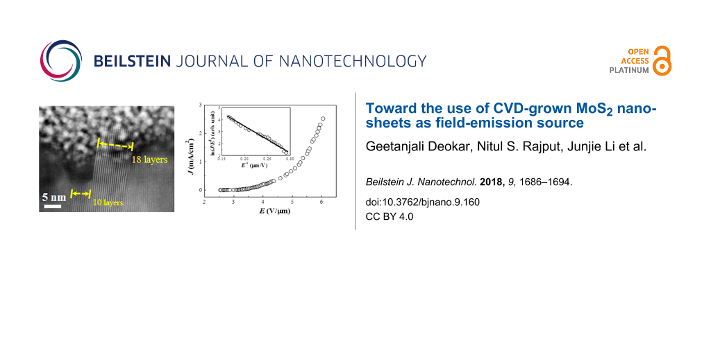
FE measurements on the transferred MoS2 NSs are given in Figure 5. The transferred NSs were checked using SEM (Figure 5c) and Raman spectroscopy (not shown as it is identical to the as-grown NSs). It was thus confirmed that they are of similar quality to that of as-grown NSs. The Fowler–Nordheim (F–N) equation [28] was modified for a cathode with nanometric field emitters as follows:
(1)
E = U/d, where U is the voltage applied between the flat cathode and the anode screen and d is the distance in between (220 µm). A and B are constants (A = 1.54 × 10⁻⁶ AeV·V−1, B = 6.83 × 10⁶ eV−3/2·Vnm−1) that depend on the surface structure. λM is a macroscopic pre-exponential correction factor. UF (the correction factor) is a particular value of the principal Schottky–Nordheim barrier function U. β is the local electrical field enhancement factor. is the work function of the emitter (considered to be 4.04 eV here [29]). In Figure 6a, the current density versus electric field (J–E) curve of the transferred MoS2 on the FTO sample is displayed. The ln(J/E2) versus 1/E graph of the emission data is shown in the inset of Figure 6a. The linear behavior indicates that FE from the NSs is dominated by the tunneling effect. It can be seen that the density of emission current increases rapidly along with the increasing of the applied electric field (Figure 6a). The turn-on field, defined at a current density of 10 µA/cm2, and the threshold field at 1 mA/cm2, are 3.1 and 5.3 V/µm, respectively. These data are found to be better than the previously reported values for MoS2 nanoflowers [13] or multilayered MoS2[8,12], and comparable with the vertically aligned MoS2 NSs with ultrathin edges in [9] (Table 1). It has been shown previously that vertically grown 1D nanowires/nanotubes and 2D NSs with atomically thin edges may considerably improve the FE properties, so that vertically standing materials are promising for FE applications [30]. The low turn-on field and threshold field of the MoS2 NSs could be due to their vertically aligned extremely thin edges, forming a nano-tip-like structure (Figure S1, Supporting Information File 1).
Figure 5:
Photographs of (a) wet chemically transferred MoS2 sample on the FTO/glass substrate, the FTO film on the glass substrate is marked with a yellow dotted square. (b) The remaining square Si sample after being detached from the MoS2 NSs after the buffered oxide etchant. The triangular sample in panel (b) is a piece from the original sample kept for TEM measurements.
Figure 5:
Photographs of (a) wet chemically transferred MoS2 sample on the FTO/glass substrate, the FTO film ...
Figure 6:
(a) Field-emission current density as a function of the electric field for the transferred MoS2 NSs on FTO/glass. The inset shows the corresponding FN plot with a linear fitting used for estimating the field-enhancement factor. (b) The long-term field-emission stability for the same sample at the pressure of ca. 10−6 mbar with luminance from the sample.
Figure 6:
(a) Field-emission current density as a function of the electric field for the transferred MoS2 NSs...
A considerable enhancement in FE can be achieved by tuning the geometrical morphology of the emitter surface and thus it is important to control the surface morphology for producing better field emitters [9,30,31]. The emitter surface is rough for nanomaterials deposited as a planar cathode and, therefore, for a given emission site the applied electric field varies from the local electric field. The ratio of the actual local electric field to the applied average electric field is known as the field-enhancement factor. In the present case, the field-enhancement factor, commonly used for evaluating FE properties, is calculated from the slope m of the F–N plot (a plot of ln(J/E2) versus 1/E as given in the inset of Figure 6a, using the following equation:
(2)
A value of 867 is estimated by linearly fitting the FN plot. This value is indeed higher than that of MoS2 nanoflowers [8,13], and in the range of few-layered MoS2 NS field emitters (β = 1138 for hydrothermally produced MoS2 NSs) [12]. The enhancement factor for our NSs is apparently smaller than the one recently reported on vertically aligned MoS2 NSs (β = 6240 for NSs with ultrathin edges) [9]. However, the electric field required to obtain a high current density of 10 µA/cm2 is much lower for our as-produced NSs as compared to the above report (Table 1). It can be seen that a high current density ≥2.5 mA/cm2 can be achieved (Figure 6a). For the sparsely distributed and ultrathin edge NSs, the current density is only 0.2 mA/cm2[9]. To obtain high current density from the material is very important for practical applications. Thus, as compared with previously published horizontally aligned monolayer or the vertically aligned MoS2 NSs or nanoflowers, the as-produced NSs present a clear advantage in terms of low turn-on field and high current density. It has been demonstrated that film morphology of the cathode greatly influences the field-emission performance and the electrons are easier to be extracted from a film with more exposed edges [32]. Hence, we believe that the tip-like geometry (Figure 1d) and exposed edges (Figure 4) of the MoS2 NSs are enhancing the tunneling probability for electrons in layered nanomaterials. A similar effect has been observed previously in carbon nanotubes [33].
The emission current density versus time plot is shown in Figure 6b. An almost stable (fluctuations between 10 and 20 µA/cm2) emission over a period of 100 min without any measurable degradation can be seen. The densely packed NSs might be playing an important role to achieve high current density and faster heat dissipation, thereby reducing the burning out of active emission sites induced by Joule heating. The as-grown NSs could also possibly be used as heat dissipating nano-channels in FE or electronic devices [34]. Moreover, the excellent luminance uniformity (except over the film area broken during the transfer process, refer to Figure 5a) of the cathode is demonstrated from the inset in Figure 6b. The stability and luminance results indicate that the as-grown material could be a good emitter in vacuum environments relevant to the industry.
Conclusion
Uniform and continuous MoS2 NSs of 5–20 nm thickness were successfully grown by CVD on SiO2/Si substrates by a double sulfurization step. Micro-Raman and XPS measurements revealed high-quality growth of the vertically aligned NSs. Cross-section TEM measurements revealed that the NSs of 5–20 nm thickness have a height of a few tens of nanometers. AFM measurements showed that the NSs formed a FE nano-tip-like morphology. We have demonstrated that the as-grown NSs can be transferred onto a desired substrate such as conducting FTO/glass employing a wet-chemical transfer process. These NSs show very interesting FE properties at room temperature and in high vacuum (10−6 mbar) as proven by the low turn-on field of 3.1 V/μm and low threshold field of 5.3 V/µm. In future, the as-grown NSs could be potentially used for FE and display device applications.
Supporting Information
Supporting Information File 1:
Additional experimental data.
Authors acknowledge Dr. Cyril Aubry for his help in AFM measurement. Part of the research leading to this work received funding from the European Union Seventh Framework Program under grant agreement No 604391 Graphene Flagship. Francis Leonard Deepak and Junjie Li thank the financial support provided by the N2020: Nanotechnology based functional solutions (NORTE-45-2015-02).
References
Zhai, T.; Li, L.; Ma, Y.; Liao, M.; Wang, X.; Fang, X.; Yao, J.; Bando, Y.; Golberg, D. Chem. Soc. Rev.2011,40, 2986–3004. doi:10.1039/c0cs00126k
Return to citation in text:
[1]
[2]
[3]
[4]
Zhang, H.; Tang, J.; Yuan, J.; Yamauchi, Y.; Suzuki, T. T.; Shinya, N.; Nakajima, K.; Qin, L.-C. Nat. Nanotechnol.2016,11, 273–279. doi:10.1038/nnano.2015.276
Return to citation in text:
[1]
[2]
Fan, S.; Chapline, M. G.; Franklin, N. R.; Tombler, T. W.; Cassell, A. M.; Dai, H. Science1999,283, 512–514. doi:10.1126/science.283.5401.512
Return to citation in text:
[1]
Zhong, H.; Yang, G.; Song, H.; Liao, Q.; Cui, H.; Shen, P.; Wang, C.-X. J. Phys. Chem. C2012,116, 9319–9326. doi:10.1021/jp301024d
Return to citation in text:
[1]
Malesevic, A.; Kemps, R.; Vanhulsel, A.; Chowdhury, M. P.; Volodin, A.; Haesendonck, C. V. J. Appl. Phys.2008,104, 084301. doi:10.1063/1.2999636
Return to citation in text:
[1]
Viskadouros, G.; Zak, A.; Stylianakis, M.; Kymakis, E.; Tenne, R.; Stratakis, E. Small2014,10, 2398–2403. doi:10.1002/smll.201303340
Return to citation in text:
[1]
Sachin, R. S.; Amit, S. P.; Mahendra, S. P.; Sandesh, R. J.; Mahendra, A. M.; Dattatray, J. L. Mater. Res. Express2016,3, 035003. doi:10.1088/2053-1591/3/3/035003
Return to citation in text:
[1]
Kashid, R. V.; Joag, P. D.; Thripuranthaka, M.; Rout, C. S.; Late, D. J.; More, M. A. Nanomater. Nanotechnol.2015,5, 10. doi:10.5772/60071
Return to citation in text:
[1]
[2]
[3]
[4]
[5]
Li, H.; Wu, H.; Yuan, S.; Qian, H. Sci. Rep.2016,6, 21171. doi:10.1038/srep21171
Return to citation in text:
[1]
[2]
[3]
[4]
[5]
[6]
[7]
[8]
[9]
[10]
Palacios, E.; Park, S.; Butun, S.; Lauhon, L.; Aydin, K. Appl. Phys. Lett.2017,111, 031101. doi:10.1063/1.4993427
Return to citation in text:
[1]
Bo, Z.; Yang, Y.; Chen, J.; Yu, K.; Yan, J.; Cen, K. Nanoscale2013,5, 5180–5204. doi:10.1039/c3nr33449j
Return to citation in text:
[1]
Kashid, R. V.; Late, D. J.; Chou, S. S.; Huang, Y.-K.; De, M.; Joag, D. S.; More, M. A.; Dravid, V. P. Small2013,9, 2730–2734. doi:10.1002/smll.201300002
Return to citation in text:
[1]
[2]
[3]
[4]
[5]
Li, Y. B.; Bando, Y.; Golberg, D. Appl. Phys. Lett.2003,82, 1962–1964. doi:10.1063/1.1563307
Return to citation in text:
[1]
[2]
[3]
[4]
[5]
Devan, R. S.; Thakare, V. P.; Antad, V. V.; Chikate, P. R.; Khare, R. T.; More, M. A.; Dhayal, R. S.; Patil, S. I.; Ma, Y.-R.; Schmidt-Mende, L. ACS Omega2017,2, 2925–2934. doi:10.1021/acsomega.7b00345
Return to citation in text:
[1]
Deokar, G.; Vignaud, D.; Arenal, R.; Louette, P.; Colomer, J.-F. Nanotechnology2016,27, 075604. doi:10.1088/0957-4484/27/7/075604
Return to citation in text:
[1]
[2]
Eda, G.; Yamaguchi, H.; Voiry, D.; Fujita, T.; Chen, M.; Chhowalla, M. Nano Lett.2011,11, 5111–5116. doi:10.1021/nl201874w
Return to citation in text:
[1]
[2]
Cho, S.-Y.; Kim, S. J.; Lee, Y.; Kim, J.-S.; Jung, W.-B.; Yoo, H.-W.; Kim, J.; Jung, H.-T. ACS Nano2015,9, 9314–9321. doi:10.1021/acsnano.5b04504
Return to citation in text:
[1]
[2]
[3]
Deokar, G.; Rajput, N. S.; Vancsó, P.; Ravaux, F.; Jouiad, M.; Vignaud, D.; Cecchet, F.; Colomer, J.-F. Nanoscale2017,9, 277–287. doi:10.1039/C6NR07965B
Return to citation in text:
[1]
[2]
[3]
Deokar, G.; Avila, J.; Razado-Colambo, I.; Codron, J.-L.; Boyaval, C.; Galopin, E.; Asensio, M.-C.; Vignaud, D. Carbon2015,89, 82–92. doi:10.1016/j.carbon.2015.03.017
Return to citation in text:
[1]
[2]
Rajput, N. S.; Kim, S.-G.; Chou, J. B.; Abed, J.; Viegas, J.; Jouiad, M. MRS Adv.2016,1, 825–830. doi:10.1557/adv.2015.20
Return to citation in text:
[1]
Lee, C.; Yan, H.; Brus, L. E.; Heinz, T. F.; Hone, J.; Ryu, S. ACS Nano2010,4, 2695–2700. doi:10.1021/nn1003937
Return to citation in text:
[1]
Kibsgaard, J.; Chen, Z.; Reinecke, B. N.; Jaramillo, T. F. Nat. Mater.2012,11, 963–969. doi:10.1038/nmat3439
Return to citation in text:
[1]
[2]
[3]
Spevack, P. A.; McIntyre, N. S. J. Phys. Chem.1993,97, 11031–11036. doi:10.1021/j100144a021
Return to citation in text:
[1]
[2]
[3]
[4]
Zhang, X.; Jia, F.; Yang, B.; Song, S. J. Phys. Chem. C2017,121, 9938–9943. doi:10.1021/acs.jpcc.7b01863
Return to citation in text:
[1]
[2]
Zhang, Z.; Zou, L.; Aubry, C.; Jouiad, M.; Hao, Z. J. Membr. Sci.2016,515, 204–211. doi:10.1016/j.memsci.2016.05.054
Return to citation in text:
[1]
Kong, D.; Wang, H.; Cha, J. J.; Pasta, M.; Koski, K. J.; Yao, J.; Cui, Y. Nano Lett.2013,13, 1341–1347. doi:10.1021/nl400258t
Return to citation in text:
[1]
Wu, Y.; Li, J.; Ye, J.; Song, Y.; Chen, X.; Huang, S.; Sun, Z.; Ou-Yang, W. J. Alloys Compd.2017,726, 675–679. doi:10.1016/j.jallcom.2017.08.026
Return to citation in text:
[1]
Lee, S. Y.; Kim, U. J.; Chung, J.; Nam, H.; Jeong, H. Y.; Han, G. H.; Kim, H.; Oh, H. M.; Lee, H.; Kim, H.; Roh, Y.-G.; Kim, J.; Hwang, S. W.; Park, Y.; Lee, Y. H. ACS Nano2016,10, 6100–6107. doi:10.1021/acsnano.6b01742
Return to citation in text:
[1]
Green, J. M.; Dong, L.; Gutu, T.; Jiao, J.; Conley, J. F., Jr.; Ono, Y. J. Appl. Phys.2006,99, 094308. doi:10.1063/1.2194112
Return to citation in text:
[1]
[2]
Wang, F.-J.; Deng, L.-N.; Deng, J.-H. Appl. Surf. Sci.2015,355, 218–225. doi:10.1016/j.apsusc.2015.07.103
Return to citation in text:
[1]
Xu, J.; Xu, P.; Ou-Yang, W.; Chen, X.; Guo, P.; Li, J.; Piao, X.; Wang, M.; Sun, Z. Appl. Phys. Lett.2015,106, 073501. doi:10.1063/1.4909552
Return to citation in text:
[1]
Fujii, S.; Honda, S.-i.; Machida, H.; Kawai, H.; Ishida, K.; Katayama, M.; Furuta, H.; Hirao, T.; Oura, K. Appl. Phys. Lett.2007,90, 153108. doi:10.1063/1.2721876
Return to citation in text:
[1]
Dwivedi, V. K.; Gopal, R.; Ahmad, S. Microelectron. J.2000,31, 405–410. doi:10.1016/S0026-2692(00)00015-X
Return to citation in text:
[1]
Kashid, R. V.; Late, D. J.; Chou, S. S.; Huang, Y.-K.; De, M.; Joag, D. S.; More, M. A.; Dravid, V. P. Small2013,9, 2730–2734. doi:10.1002/smll.201300002
Kashid, R. V.; Joag, P. D.; Thripuranthaka, M.; Rout, C. S.; Late, D. J.; More, M. A. Nanomater. Nanotechnol.2015,5, 10. doi:10.5772/60071
12.
Kashid, R. V.; Late, D. J.; Chou, S. S.; Huang, Y.-K.; De, M.; Joag, D. S.; More, M. A.; Dravid, V. P. Small2013,9, 2730–2734. doi:10.1002/smll.201300002
Lee, S. Y.; Kim, U. J.; Chung, J.; Nam, H.; Jeong, H. Y.; Han, G. H.; Kim, H.; Oh, H. M.; Lee, H.; Kim, H.; Roh, Y.-G.; Kim, J.; Hwang, S. W.; Park, Y.; Lee, Y. H. ACS Nano2016,10, 6100–6107. doi:10.1021/acsnano.6b01742
Kashid, R. V.; Late, D. J.; Chou, S. S.; Huang, Y.-K.; De, M.; Joag, D. S.; More, M. A.; Dravid, V. P. Small2013,9, 2730–2734. doi:10.1002/smll.201300002
Devan, R. S.; Thakare, V. P.; Antad, V. V.; Chikate, P. R.; Khare, R. T.; More, M. A.; Dhayal, R. S.; Patil, S. I.; Ma, Y.-R.; Schmidt-Mende, L. ACS Omega2017,2, 2925–2934. doi:10.1021/acsomega.7b00345
Kashid, R. V.; Late, D. J.; Chou, S. S.; Huang, Y.-K.; De, M.; Joag, D. S.; More, M. A.; Dravid, V. P. Small2013,9, 2730–2734. doi:10.1002/smll.201300002
Sachin, R. S.; Amit, S. P.; Mahendra, S. P.; Sandesh, R. J.; Mahendra, A. M.; Dattatray, J. L. Mater. Res. Express2016,3, 035003. doi:10.1088/2053-1591/3/3/035003
Kashid, R. V.; Late, D. J.; Chou, S. S.; Huang, Y.-K.; De, M.; Joag, D. S.; More, M. A.; Dravid, V. P. Small2013,9, 2730–2734. doi:10.1002/smll.201300002


![[2190-4286-9-160-1]](/bjnano/content/figures/2190-4286-9-160-1.png?scale=1.8&max-width=1024&background=FFFFFF)
![[2190-4286-9-160-2]](/bjnano/content/figures/2190-4286-9-160-2.png?scale=2.0&max-width=1024&background=FFFFFF)
![[2190-4286-9-160-3]](/bjnano/content/figures/2190-4286-9-160-3.png?scale=2.0&max-width=1024&background=FFFFFF)
![[2190-4286-9-160-4]](/bjnano/content/figures/2190-4286-9-160-4.png?scale=2.0&max-width=1024&background=FFFFFF)
![[2190-4286-9-160-i1]](/bjnano/content/inline/2190-4286-9-160-i1.svg?max-width=590&scale=1.18182)
![[Graphic 1]](/bjnano/content/inline/2190-4286-9-160-i3.svg?max-width=637&scale=1.18182) is the work function of the emitter (considered to be 4.04 eV here [29]). In Figure 6a, the current density versus electric field (J–E) curve of the transferred MoS2 on the FTO sample is displayed. The ln(J/E2) versus 1/E graph of the emission data is shown in the inset of Figure 6a. The linear behavior indicates that FE from the NSs is dominated by the tunneling effect. It can be seen that the density of emission current increases rapidly along with the increasing of the applied electric field (Figure 6a). The turn-on field, defined at a current density of 10 µA/cm2, and the threshold field at 1 mA/cm2, are 3.1 and 5.3 V/µm, respectively. These data are found to be better than the previously reported values for MoS2 nanoflowers [13] or multilayered MoS2 [8,12], and comparable with the vertically aligned MoS2 NSs with ultrathin edges in [9] (Table 1). It has been shown previously that vertically grown 1D nanowires/nanotubes and 2D NSs with atomically thin edges may considerably improve the FE properties, so that vertically standing materials are promising for FE applications [30]. The low turn-on field and threshold field of the MoS2 NSs could be due to their vertically aligned extremely thin edges, forming a nano-tip-like structure (Figure S1, Supporting Information File 1).
is the work function of the emitter (considered to be 4.04 eV here [29]). In Figure 6a, the current density versus electric field (J–E) curve of the transferred MoS2 on the FTO sample is displayed. The ln(J/E2) versus 1/E graph of the emission data is shown in the inset of Figure 6a. The linear behavior indicates that FE from the NSs is dominated by the tunneling effect. It can be seen that the density of emission current increases rapidly along with the increasing of the applied electric field (Figure 6a). The turn-on field, defined at a current density of 10 µA/cm2, and the threshold field at 1 mA/cm2, are 3.1 and 5.3 V/µm, respectively. These data are found to be better than the previously reported values for MoS2 nanoflowers [13] or multilayered MoS2 [8,12], and comparable with the vertically aligned MoS2 NSs with ultrathin edges in [9] (Table 1). It has been shown previously that vertically grown 1D nanowires/nanotubes and 2D NSs with atomically thin edges may considerably improve the FE properties, so that vertically standing materials are promising for FE applications [30]. The low turn-on field and threshold field of the MoS2 NSs could be due to their vertically aligned extremely thin edges, forming a nano-tip-like structure (Figure S1, Supporting Information File 1).![[2190-4286-9-160-5]](/bjnano/content/figures/2190-4286-9-160-5.png?scale=2.0&max-width=1024&background=FFFFFF)
![[2190-4286-9-160-6]](/bjnano/content/figures/2190-4286-9-160-6.png?scale=2.0&max-width=1024&background=FFFFFF)
![[2190-4286-9-160-i2]](/bjnano/content/inline/2190-4286-9-160-i2.svg?max-width=590&scale=1.18182)