Department of Physics, Quantum-Functional Semiconductor Research Center, Nano Information Technology Academy, Dongguk University, 3-26 Pildong, Junggu, 100-715, Seoul, Korea
Department of Physics, Quantum-Functional Semiconductor Research Center, Nano Information Technology Academy, Dongguk University, 3-26 Pildong, Junggu, 100-715, Seoul, Korea
Department of Physics, Quantum-Functional Semiconductor Research Center, Nano Information Technology Academy, Dongguk University, 3-26 Pildong, Junggu, 100-715, Seoul, Korea
Department of Physics, Quantum-Functional Semiconductor Research Center, Nano Information Technology Academy, Dongguk University, 3-26 Pildong, Junggu, 100-715, Seoul, Korea
Institute for Microelectronics Technology & High Purity Materials, RAS, 142432 Chernogolovka, Moscow district, Russia
1Belarusian State University, 4 Nezavisimosti Av., 220030 Minsk, Belarus
2Department of Chemistry, Moscow State University, Leninskie Gory, 1, b.3, 119991, Moscow, Russia
3Department of Physics, Quantum-Functional Semiconductor Research Center, Nano Information Technology Academy, Dongguk University, 3-26 Pildong, Junggu, 100-715, Seoul, Korea
4Institute for Microelectronics Technology & High Purity Materials, RAS, 142432 Chernogolovka, Moscow district, Russia
Corresponding author email
§ Phone +375172095451; Fax +375172095445
Associate Editor: A. J. Meixner Beilstein J. Nanotechnol.2018,9, 704–710.https://doi.org/10.3762/bjnano.9.65 Received 04 Oct 2017,
Accepted 23 Jan 2018,
Published 22 Feb 2018
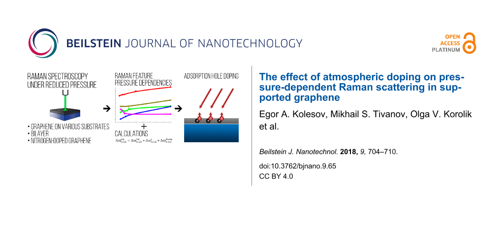
Atmospheric doping of supported graphene was investigated by Raman scattering under different pressures. Various Raman spectra parameters were found to depend on the pressure and the substrate material. The results are interpreted in terms of atmospheric adsorption leading to a change in graphene charge carrier density and the effect of the substrate on the electronic and phonon properties of graphene. It was found that adsorption of molecules from the atmosphere onto graphene doped with nitrogen (electron doping) compensates for the electron charge. Furthermore, the atmosphere-induced doping drastically decreases the spatial heterogeneity of charge carriers in graphene doped with nitrogen, while the opposite effect was observed for undoped samples. The results of this study should be taken into account for the development of sensors and nanoelectronic devices based on graphene.
Graphene is a promising material for a variety of applications due to its unique physical properties [1]. Among its other outstanding features, one can distinguish its strong sensitivity to adsorbates, leading to a huge number of potential graphene applications in biosensors [2]. Atmospheric adsorption is known to affect graphene charge carrier density, leading to gradual self-sustained hole doping [3]. On one hand, adsorption can thus be an extremely undesirable effect when a nanoelectronic device is designed to operate on the basis of undoped properties of graphene; on the other hand, the adsorption of certain functional groups, for example, can be used as a constituent part of the methods of graphene functionalization [4]. At the same time, graphene layers on substrates are necessary for nanoelectronics. The substrates may affect the adsorption of graphene, either enhancing it, an effect very useful for biosensor applications [2], or reducing it, which is desirable when undoped graphene is needed as a device functional element.
A natural way for probing the adsorption properties of graphene is to conduct experiments under a low-pressure environment. Various high-pressure measurements for graphene are presented in the literature [5,6], while to the best of our knowledge, the studies of graphene’s response to pressure variations below atmospheric values are absent to date. As the pressure decreases, both graphene and the substrate will expand, and thus, the expected changes in the properties of graphene will not be only related to graphene’s compressibility, but also to strain caused by different compressibility values for graphene and the substrate. The authors of [5] have provided a convenient expression for compressibility-induced changes, while strain-related changes can be treated in a similar way to the thermal expansion description for supported graphene [7,8], where the strain is caused by a difference of thermal expansion coefficients for graphene and the substrate. Besides, monomers and functional groups adsorbed from the atmosphere are expected to become at least partially removed from the graphene surface as the pressure decreases, leading to changes in atmosphere-induced doping of the material [3]. A study of the characteristics of these processes may provide useful information about the adsorption properties of supported graphene.
Raman spectroscopy is a versatile tool for studying graphene and graphene-based nanomaterials [9-12]. Several different parameters of graphene’s Raman spectra are affected by charge carrier density variations, such as the G and 2D peak positions and the ratio of the 2D and G peak maximum intensities [13]. Since the sensitivity of these parameters to doping takes place due to fundamentally different processes, using a set of these parameters provides the possibility to accurately determine charge carrier density variations and distinguish the latter against, for example, substrate-induced strain effects [14,15].
The purpose of this study is to investigate the pressure-dependent behavior of the density of charge carriers in graphene and the effect of the substrate on the adsorption properties of graphene at pressures below atmospheric pressure.
Results and Discussion
Pressure-dependent Raman measurements
Raman spectra of graphene on various substrates under atmospheric pressure are presented in Figure 1. Monolayer and bilayer graphene were identified by 2D peak approximations with one and four Lorentz functions, respectively, together with the 2D peak full-width at half-maximums (FWHMs). The I2D/IG intensity ratio shows values of up to 1.5 for the monolayer and about 0.9 for bilayer graphene (the low I2D/IG values can be explained by adsorption doping [9] and electrostatic doping effects [16], as analyzed throughout the article).
Figure 1:
Raman spectra of graphene on various substrates, as well as bilayer and nitrogen-doped graphene.
Figure 1:
Raman spectra of graphene on various substrates, as well as bilayer and nitrogen-doped graphene.
Comparing the spectra for as-grown and transferred graphene on copper, one can distinguish the upshifted positions of the G and 2D peaks. The stronger upshift for as-grown graphene (by 20–23 cm−1 with respect to normal positions) can be attributed to several effects: substrate-induced strain [14,15], hole doping by adsorbates [13], and substrate-induced electrostatic doping [16]. The G and 2D peak positions upshifted by 5–8 cm−1 and the considerably low I2D/IG ratio of 1.3–1.4 for graphene transferred onto copper and Al2O3 could be explained by similar effects, which in this case, tend to be less pronounced after the transfer. For doped graphene (1.11% of nitrogen from XPS data), the D band intensity increases compared to pristine graphene, the second disorder-induced peak (the D’ band) also becomes evident, the G peak position is upshifted by ≈3 cm−1, while the 2D peak is about normal, naturally indicating electron doping together with I2D/IG values of 1.4–1.6 [13].
Figure 2 shows pressure-dependent G and 2D peak shifts, typical for different samples, with respect to normal positions of about 1582 and 2676 cm−1 for a 532 nm laser, respectively. Downshift was commonly observed for undoped graphene peaks as the pressure decreased, while for nitrogen-doped graphene, the G peak position value increased. The 2D peak remained unchanged throughout the whole pressure range. Besides, changes of the I2D/IG intensity ratio were observed as the pressure decreased, indicating variations of graphene charge carrier density [13]. After the atmosphere was returned to that of the pressure-controlled box, the spectra parameters gradually changed back to their initial values over a period of up to four days of air exposure.
Figure 2:
Pressure-dependent G and 2D peak position shifts for graphene on various substrates, as well as bilayer and nitrogen-doped graphene. Symbols show the experimental points, and solid lines represent general trends of peak shift.
Figure 2:
Pressure-dependent G and 2D peak position shifts for graphene on various substrates, as well as bil...
Theoretical estimation of different process contributions to the observed shift
The G and 2D peak experimental pressure shift can be explained by changes in the corresponding phonon mode energy due to (1) graphene lattice compressibility [5], (2) strain induced by the difference of compressibility values for graphene and substrate [5,14], and (3) possible desorption of atmosphere-induced doping groups [3,13]. Thus, the experimental peak shift due to pressure change can be written as:
(1)
The first term is defined by the following expression [5]:
(2)
where and are normal G and 2D peak positions, respectively; γG,2D is a Grüneisen parameter for corresponding E2g and A1g phonon modes (values of 1.8 and 2.7 were used, respectively [14]), a is the graphene atomic bond length (a0 under zero-pressure conditions). As it was shown in [5], a relationship for graphite in-plane compressibility from [17] is applicable for a(p)/a0 estimation:
(3)
where
is the linear compressibility and β' is its pressure derivative. In the present study, β0 and β' values of 1250 GPa and 1 were used, respectively [17].
The strain-induced shift, by analogy with thermal expansion strain [7,8,18], can be written as:
(4)
where
is a biaxial strain rate (in our calculations we used the values of −58 and −144 cm−1/% for G and 2D peak, respectively [14]), ε is a relative deformation (%), and r is a substrate atomic bond length.
In [5] it was shown that at low pressure the r(p)/r0 relation can be approximately defined through the substrate bulk modulus B0 in the following way:
(5)
A value for the doping contribution can on one hand be calculated from Equation 1 using the obtained experimental shift values; on the other hand, in can be obtained from other doping-dependent Raman spectra parameters that are not commonly referred to as strain-dependent, such as I2D/IG intensity ratio [13].
During the calculation, it turned out that the graphene lattice compression contribution does not lead to a substantial change in the G and 2D peak positions – less than 10−2 cm−1 as the pressure changes from 0 to 1 atm (≈1·105 Pa). The same is valid for the strain-induced shift (less than 10−3 cm−1 for graphene on all substrates). Since these results dramatically exclude the first two terms from Equation 1, we assume the experimental shift to be caused by changes in graphene doping.
Carrier density variation analysis
Table 1 demonstrates the carrier density change ∆n obtained from Raman spectra [13] of various graphene samples as the pressure decreased, as well as Raman feature parameters at normal and reduced pressures. As can be seen, greater ∆n values were obtained for nitrogen-doped graphene, while for bilayers on SiO2/Si and graphene transferred to copper, weaker desorption occurred. It is important to note that doping has various effects on the Raman spectral parameters [13]: stronger doping is expressed as lower I2D/IG ratio values, while the G and 2D peak positions depend on carrier density non-linearly.
Table 1:
Summarized Raman spectra parameters and resultant doping change as the pressure decreased from normal to reduced pressure for various graphene samples. For all samples except the nitrogen-doped graphene, ∆n indicates a hole density decrease (removal of hole-inducing adsorbates from the sample surface). For doped graphene, it corresponds to an increase of electron density (similar desorption process that cancel the balancing role of adsorbed groups).
Sample
Pressure, mbar
Pos(G), cm−1
Pos(2D), cm−1
I2D/IG
∆n, ×1013 cm−2
graphene on copper (as-grown)
1000
1605
2696
0.9
≈0.6–0.9 (hole doping)
5 × 10⁻⁵
1599
2691
1.2
graphene on copper (transferred)
1000
1590
2681
1.3
≈0.3–0.5 (hole doping)
5 × 10⁻⁵
1586
2676
1.6
graphene on Al2O3
1000
1590
2681
1.4
≈0.5–0.8 (hole doping)
5 × 10⁻⁵
1582a
2674a
2.3a
doped graphene on SiO2/Si
1000
1585
2679
1.5
≈0.7–1.0 (electron doping)
5 × 10⁻⁵
1588
2679
1.2
bilayer on SiO2/Si
1000
1594
2682
0.9
≈0.3–0.5 (hole doping)
5 × 10⁻⁵
1590
2676
1.0
aThe closest to normal graphene peak positions as well as greater I2D/IG values were observed for graphene on Al2O3 at reduced pressure.
In order to analyze the obtained results, we first compare the peak position shift for pristine and transferred graphene on Cu in Figure 2, where one can notice a similar behavior up to a certain constant. A considerable similarity of the peak position downshift indicates analogous kinetics of adsorbate removal from graphene surface. However, a different intercept leads to a 13–15 cm−1 distance between the plots. This observation can be explained by substrate-induced strain in as-grown graphene (leading to greater overall peak positions [14]): The van der Waals graphene–substrate interaction model may not be fully applicable for this case due to the possibility of chemical bonds present between graphene and copper [19] which are terminated after the transfer. Besides, this may lead to different values of the average graphene–substrate distance resulting in deviation of the density of states (DOS) from a simple Dirac cone [16] and a consequent shift of the Dirac point energy, leading to different substrate-induced doping that affects all Raman features related to carrier density but most likely do not change with the pressure (smaller overall values of I2D/IG intensity ratio). This explains the similar shift but different intercept for pristine and transferred graphene on Cu in Figure 2.
Comparing graphene transferred to Cu and Al2O3 as typical conducting and dielectric materials, a stronger carrier density change was obtained for the latter. As the pressure decreases, removal of adsorbates from the surface of graphene on Al2O3 results in the Raman spectra parameters becoming close to those typical for completely undoped graphene [13] – in particular, the strong I2D/IG increase seen in Table 1 should be noted. At the same time, a smaller hole density decrease for graphene transferred to Cu can be explained by analogy with as-grown graphene by stronger graphene–substrate interaction in this case (interaction energy of 0.72 J/m2 against ≈0.47 J/m2 for graphene on Al2O3 substrate [20,21]) and therefore more pronounced substrate-induced doping [16]. Besides, the electrostatic screening of the electron–electron interaction for graphene on a metallic substrate [22,23] can contribute. The screening effect results in renormalization of the Fermi velocity, Dirac point velocity, and overall distortion of the Dirac cone [24], leading to a possible charge carrier density increase [25].
In the case of bilayer graphene, the desorption process leads to a density decrease of about 0.4 × 1013 cm−2 hole, which is close to the case of graphene transferred to Cu. Being a van der Waals structure on the scale of adsorption effects (in terms of interlayer bonding), bilayer graphene is known to have a slightly greater energy barrier for the adsorption process [26]. However, adsorption in this case can also lead to at least partial layer decoupling that results in the presence of biaxial strain [27]. Besides, values of I2D/IG did not indicate a strong doping presence. Thus, the overall greater G and 2D peak position values most likely are strain-related rather than an indication of greater atmosphere-induced doping.
A very interesting situation is observed for nitrogen-doped graphene. The results of pressure-dependent studies presented in Figure 2 have shown a G peak upshift, while the 2D peak position remained unchanged. This behavior together with the change of I2D/IG corresponds to an increase of electron density, according to dependencies presented in [13]. This fact leads to an interesting conclusion that adsorption hole doping most likely counterbalances electron concentration in nitrogen-doped graphene. A greater change of the carrier density within the experimental pressure range compared to undoped graphene indicates that under electronic doping more active adsorption occurs, balancing the “excess” electron density through opposite-sign charge carrier introduction and subsequent recombination, and moving the Fermi level position closer to a normal value.
As seen from Figure 3a, in addition to an upshift, the initially distorted G peak at normal pressure experiences stronger profile distortion as the pressure decreases, with the most asymmetric profile corresponding to the lowest pressure. This fact indicates that as desorption occurs, inhomogeneity of the charge carrier distribution increases, approaching conditions typical for doped graphene [28]. Thus, atmospheric adsorption not only counterbalances the excess electron concentration, but also reduces the charge carrier inhomogeneity, with the whole system evolving closer to equilibrium.
Figure 3:
G peak profile for (a) nitrogen-doped graphene on SiO2/Si and (b) graphene on Al2O3 at normal and reduced pressures.
Figure 3:
G peak profile for (a) nitrogen-doped graphene on SiO2/Si and (b) graphene on Al2O3 at normal and r...
It is important to note that the opposite situation was observed for undoped graphene: as the pressure decreased (with desorption leading to doping decrease), the G peak (in addition to the downshift) evolved from a distorted lineshape at normal pressure to an almost symmetric one in vacuum (≈5 × 10⁻⁵ mbar), as seen in Figure 3b. This fact means that the effect of atmospheric adsorption that reduces charge carrier inhomogeneity in graphene is quite unique for the electron-doped graphene case, while the inverse process is naturally typical for the pure material, as it was previously noted [28].
The results presented above demonstrate that pressure-dependent Raman spectroscopy is a convenient tool for probing atmosphere-induced doping in graphene. Low-pressure behavior of adsorbates present on the graphene surface and concomitant charge carrier properties strongly depend on the substrate material, as well as graphene doping and number of layers. These results can be taken into account during the development of any graphene-related devices, either specifically involving graphene adsorption properties (for example, biosensors) or assuming exposure of air to the device functional elements.
Conclusion
Pressure-dependent Raman spectroscopy studies in the range from 1000 to 5 × 10⁻⁵ mbar of supported graphene have shown that the G and 2D peak positions and the ratio of the 2D and G peak intensities change with the pressure, whereby the substrate material affects the dependencies. Performed calculations showed negligible lattice compressibility and strain contributions to the observed effect, and thus the shift was fully attributed to atmosphere-induced adsorption doping. During the analysis, the effect of the substrate on graphene electronic and phonon properties was taken into account. For nitrogen-doped graphene (electronic doping), adsorption was found to counterbalance the excess charge carriers. In addition, it turned out that atmosphere-induced doping decreases charge carrier inhomogeneity in nitrogen-doped graphene. For the undoped graphene samples, the opposite effect occurs. The results of the present study are useful for graphene-based sensor design, graphene functionalization techniques, and taking into account adsorption effects during nanoelectronic device engineering.
Experimental
Graphene was synthesized on Cu foil at 1020 °C by a chemical vapor deposition (CVD) method using a mixture of CH4 of 40 sccm and H2 of 10 sccm. Cu foil (Alfa Aesar, 99.999%, 10 × 30 cm2, 25 μm thick) was pre-annealed at 1060 °C with a hydrogen flow of 300 sccm and an argon flow of 2,000 sccm at a pressure of <10−4 Torr for 1–2 hours inside the chamber. After the growth of graphene, the Cu foil was cooled to room temperature. The cooling rate was described in detail elsewhere [29].
The grown graphene was transferred to various substrates using a “PMMA-mediated” method [30]. PMMA (molecular weight = 996 000, dissolved in anisole) was spin-coated (3000 rpm, 1 min) on graphene supported by Cu foil. A 0.1 M (NH4)2S2O8 aqueous solution was used to etch Cu and a water/isopropyl alcohol mixture was used to wash graphene from etching products [31]. PMMA was removed by submerging the sample in glacial acetic acid (extra pure) [32] for 4 h.
Graphene, doped with nitrogen, was prepared using a nitrogen-plasma treatment described elsewhere [33].
The Raman spectra were obtained with a confocal Raman spectrometer Nanofinder HE (LOTIS TII) with a spectral resolution better than 3 cm−1. For the excitation of Raman radiation, a continuous wave solid-state laser with a wavelength of 532 nm was used. During low-pressure Raman measurements, the sample was studied in a pressure-controlled box (pressure ranged from 1000 to about 5 × 10⁻⁵ mbar). A laser power of 2 mW was used, and the laser spot diameter was about 1.5 µm. Pressure-dependent measurements were carried out in a typical graphene monolayer and a bilayer low-defect region.
Acknowledgements
This work was supported by Belarusian State Program for Research "Photonics, opto- and microelectronics" and Russian Foundation of Basic Researches (individual project 16-33-60229), as well as partially supported by Basic Science Research Program through the National Research Foundation of Korea (NRF) funded by the Ministry of Education (ME) (No. 2017R1D1A1B03035102 and the International Research and Development program of NRF funded by the MEST (2017R1D1A1B03032759). The authors of this work are grateful to Ivan A. Svito for his help in organizing the experiment, and Prof. L.V. Yashina and Ph.D. Student A. I. Belova for XPS studies of nitrogen-doped graphene. This work was performed using equipment purchased within the Program of Development of the Lomonosov Moscow State University.
References
Zhu, Y.; Murali, S.; Cai, W.; Li, X.; Suk, J. W.; Potts, J. R.; Ruoff, R. S. Adv. Mater.2010,22, 3906–3924. doi:10.1002/adma.201001068
Return to citation in text:
[1]
Shao, Y.; Wang, J.; Wu, H.; Liu, J.; Aksay, I. A.; Lin, Y. Electroanalysis2010,22, 1027–1036. doi:10.1002/elan.200900571
Return to citation in text:
[1]
[2]
Ryu, S.; Liu, L.; Berciaud, S.; Yu, Y.-J.; Liu, H.; Kim, P.; Flynn, G. W.; Brus, L. E. Nano Lett.2010,10, 4944–4951. doi:10.1021/nl1029607
Return to citation in text:
[1]
[2]
[3]
Chen, L.; Li, J.; Li, D.; Wei, M.; Wang, X. Solid State Commun.2012,152, 1985–1989. doi:10.1016/j.ssc.2012.04.054
Return to citation in text:
[1]
Proctor, J. E.; Gregoryanz, E.; Novoselov, K. S.; Lotya, M.; Coleman, J. N.; Halsall, M. P. Phys. Rev. B2009,80, 073408. doi:10.1103/PhysRevB.80.073408
Return to citation in text:
[1]
[2]
[3]
[4]
[5]
[6]
[7]
Filintoglou, K.; Papadopoulos, N.; Arvanitidis, J.; Christofilos, D.; Frank, O.; Kalbac, M.; Parthenios, J.; Kalosakas, G.; Galiotis, C.; Papagelis, K. Phys. Rev. B2013,88, 045418. doi:10.1103/PhysRevB.88.045418
Return to citation in text:
[1]
Tivanov, M. S.; Kolesov, E. A.; Praneuski, A. G.; Korolik, O. V.; Saad, A. M.; Komissarov, I. V.; Kovalchuk, N. G. J. Mater. Sci.: Mater. Electron.2016,27, 8879–8883. doi:10.1007/s10854-016-4913-7
Return to citation in text:
[1]
[2]
Kolesov, E. A.; Tivanov, M. S.; Korolik, O. V.; Saad, A. M.; Komissarov, I. V. Carbon2017,111, 587–591. doi:10.1016/j.carbon.2016.10.020
Return to citation in text:
[1]
[2]
Ferrari, A. C.; Basko, D. M. Nat. Nanotechnol.2013,8, 235–246. doi:10.1038/nnano.2013.46
Return to citation in text:
[1]
[2]
Manikandan, E.; Kavitha, G.; Kennedy, J. Ceram. Int.2014,40, 16065–16070. doi:10.1016/j.ceramint.2014.07.129
Return to citation in text:
[1]
Kaviyarasu, K.; Manikandan, E.; Kennedy, J.; Maaza, M. J. Mater. Sci.: Mater. Electron.2016,27, 13080–13085. doi:10.1007/s10854-016-5451-z
Return to citation in text:
[1]
Kaviyarasu, K.; Maria Magdalane, C.; Manikandan, E.; Jayachandran, M.; Ladchumananandasivam, R.; Neelamani, S.; Maaza, M. Int. J. Nanosci.2015,14, 1550007. doi:10.1142/S0219581X15500076
Return to citation in text:
[1]
Beams, R.; Cançado, L. G.; Novotny, L. J. Phys.: Condens. Matter2015,27, 083002. doi:10.1088/0953-8984/27/8/083002
Return to citation in text:
[1]
[2]
[3]
[4]
[5]
[6]
[7]
[8]
[9]
[10]
Mohiuddin, T. M. G.; Lombardo, A.; Nair, R. R.; Bonetti, A.; Savini, G.; Jalil, R.; Bonini, N.; Basko, D. M.; Galiotis, C.; Marzari, N.; Novoselov, K. S.; Geim, A. K.; Ferrari, A. C. Phys. Rev. B2009,79, 205433. doi:10.1103/PhysRevB.79.205433
Return to citation in text:
[1]
[2]
[3]
[4]
[5]
[6]
Frank, O.; Vejpravova, J.; Holy, V.; Kavan, L.; Kalbac, M. Carbon2014,68, 440–451. doi:10.1016/j.carbon.2013.11.020
Return to citation in text:
[1]
[2]
Ulstrup, S.; Bianchi, M.; Hatch, R.; Guan, D.; Baraldi, A.; Alfè, D.; Hornekær, L.; Hofmann, P. Phys. Rev. B2012,86, 161402. doi:10.1103/PhysRevB.86.161402
Return to citation in text:
[1]
[2]
[3]
[4]
Hanfland, M.; Beister, H.; Syassen, K. Phys. Rev. B1989,39, 12598. doi:10.1103/PhysRevB.39.12598
Return to citation in text:
[1]
[2]
Yoon, D.; Son, Y.-W.; Cheong, H. Nano Lett.2011,11, 3227–3231. doi:10.1021/nl201488g
Return to citation in text:
[1]
Das, S.; Lahiri, D.; Lee, D.-Y.; Agarwal, A.; Choi, W. Carbon2013,59, 121–129. doi:10.1016/j.carbon.2013.02.063
Return to citation in text:
[1]
He, Y.; Chen, W. F.; Yu, W. B.; Ouyang, G.; Yang, G. W. Sci. Rep.2013,3, 2660. doi:10.1038/srep02660
Return to citation in text:
[1]
Endlich, M.; Molina-Sánchez, A.; Wirtz, L.; Kröger, J. Phys. Rev. B2013,88, 205403. doi:10.1103/PhysRevB.88.205403
Return to citation in text:
[1]
Siegel, D. A.; Hwang, C.; Fedorov, A. V.; Lanzara, A. New J. Phys.2012,14, 095006. doi:10.1088/1367-2630/14/9/095006
Return to citation in text:
[1]
Siegel, D. A.; Regan, W.; Fedorov, A. V.; Zettl, A.; Lanzara, A. Phys. Rev. Lett.2013,110, 146802. doi:10.1103/PhysRevLett.110.146802
Return to citation in text:
[1]
Li, J.; Tan, L. Z.; Zou, K.; Stabile, A. A.; Seiwell, D. J.; Watanabe, K.; Taniguchi, T.; Louie, S. G.; Zhu, J. Phys. Rev. B2016,94, 161406. doi:10.1103/PhysRevB.94.161406
Return to citation in text:
[1]
Santos, H.; Henrard, L. J. Phys. Chem. C2014,118, 27074–27080. doi:10.1021/jp507178f
Return to citation in text:
[1]
Chacón-Torres, J. C.; Wirtz, L.; Pichler, T. ACS Nano2013,7, 9249–9259. doi:10.1021/nn403885k
Return to citation in text:
[1]
Casiraghi, C.; Pisana, S.; Novoselov, K. S.; Geim, A. K.; Ferrari, A. C. Appl. Phys. Lett.2007,91, 233108. doi:10.1063/1.2818692
Return to citation in text:
[1]
[2]
Güneş, F.; Han, G. H.; Kim, K. K.; Kim, E. S.; Chae, S. J.; Park, M. H.; Jeong, H.-K.; Lim, S. C.; Lee, Y. H. Nano2009,4, 83. doi:10.1142/S1793292009001538
Return to citation in text:
[1]
Liang, X.; Sperling, B. A.; Calizo, I.; Cheng, G.; Hacker, C. A.; Zhang, Q.; Obeng, Y.; Yan, K.; Peng, H.; Li, Q.; Zhu, X.; Yuan, H.; Hight Walker, A. R.; Liu, Z.; Peng, L.-m.; Richter, C. A. ACS Nano2011,5, 9144–9153. doi:10.1021/nn203377t
Return to citation in text:
[1]
Gao, L.; Ni, G.-X.; Liu, Y.; Liu, B.; Castro Neto, A. H.; Loh, K. P. Nature2014,505, 190–194. doi:10.1038/nature12763
Return to citation in text:
[1]
Wang, H.; Maiyalagan, T.; Wang, X. ACS Catal.2012,2, 781–794. doi:10.1021/cs200652y
Return to citation in text:
[1]
References 7,8,18
7.
Tivanov, M. S.; Kolesov, E. A.; Praneuski, A. G.; Korolik, O. V.; Saad, A. M.; Komissarov, I. V.; Kovalchuk, N. G. J. Mater. Sci.: Mater. Electron.2016,27, 8879–8883. doi:10.1007/s10854-016-4913-7
8.
Kolesov, E. A.; Tivanov, M. S.; Korolik, O. V.; Saad, A. M.; Komissarov, I. V. Carbon2017,111, 587–591. doi:10.1016/j.carbon.2016.10.020
18.
Yoon, D.; Son, Y.-W.; Cheong, H. Nano Lett.2011,11, 3227–3231. doi:10.1021/nl201488g
Mohiuddin, T. M. G.; Lombardo, A.; Nair, R. R.; Bonetti, A.; Savini, G.; Jalil, R.; Bonini, N.; Basko, D. M.; Galiotis, C.; Marzari, N.; Novoselov, K. S.; Geim, A. K.; Ferrari, A. C. Phys. Rev. B2009,79, 205433. doi:10.1103/PhysRevB.79.205433
Proctor, J. E.; Gregoryanz, E.; Novoselov, K. S.; Lotya, M.; Coleman, J. N.; Halsall, M. P. Phys. Rev. B2009,80, 073408. doi:10.1103/PhysRevB.80.073408
Mohiuddin, T. M. G.; Lombardo, A.; Nair, R. R.; Bonetti, A.; Savini, G.; Jalil, R.; Bonini, N.; Basko, D. M.; Galiotis, C.; Marzari, N.; Novoselov, K. S.; Geim, A. K.; Ferrari, A. C. Phys. Rev. B2009,79, 205433. doi:10.1103/PhysRevB.79.205433
Güneş, F.; Han, G. H.; Kim, K. K.; Kim, E. S.; Chae, S. J.; Park, M. H.; Jeong, H.-K.; Lim, S. C.; Lee, Y. H. Nano2009,4, 83. doi:10.1142/S1793292009001538
Mohiuddin, T. M. G.; Lombardo, A.; Nair, R. R.; Bonetti, A.; Savini, G.; Jalil, R.; Bonini, N.; Basko, D. M.; Galiotis, C.; Marzari, N.; Novoselov, K. S.; Geim, A. K.; Ferrari, A. C. Phys. Rev. B2009,79, 205433. doi:10.1103/PhysRevB.79.205433
Tivanov, M. S.; Kolesov, E. A.; Praneuski, A. G.; Korolik, O. V.; Saad, A. M.; Komissarov, I. V.; Kovalchuk, N. G. J. Mater. Sci.: Mater. Electron.2016,27, 8879–8883. doi:10.1007/s10854-016-4913-7
8.
Kolesov, E. A.; Tivanov, M. S.; Korolik, O. V.; Saad, A. M.; Komissarov, I. V. Carbon2017,111, 587–591. doi:10.1016/j.carbon.2016.10.020
Mohiuddin, T. M. G.; Lombardo, A.; Nair, R. R.; Bonetti, A.; Savini, G.; Jalil, R.; Bonini, N.; Basko, D. M.; Galiotis, C.; Marzari, N.; Novoselov, K. S.; Geim, A. K.; Ferrari, A. C. Phys. Rev. B2009,79, 205433. doi:10.1103/PhysRevB.79.205433
Proctor, J. E.; Gregoryanz, E.; Novoselov, K. S.; Lotya, M.; Coleman, J. N.; Halsall, M. P. Phys. Rev. B2009,80, 073408. doi:10.1103/PhysRevB.80.073408
Proctor, J. E.; Gregoryanz, E.; Novoselov, K. S.; Lotya, M.; Coleman, J. N.; Halsall, M. P. Phys. Rev. B2009,80, 073408. doi:10.1103/PhysRevB.80.073408
Kaviyarasu, K.; Manikandan, E.; Kennedy, J.; Maaza, M. J. Mater. Sci.: Mater. Electron.2016,27, 13080–13085. doi:10.1007/s10854-016-5451-z
12.
Kaviyarasu, K.; Maria Magdalane, C.; Manikandan, E.; Jayachandran, M.; Ladchumananandasivam, R.; Neelamani, S.; Maaza, M. Int. J. Nanosci.2015,14, 1550007. doi:10.1142/S0219581X15500076
Mohiuddin, T. M. G.; Lombardo, A.; Nair, R. R.; Bonetti, A.; Savini, G.; Jalil, R.; Bonini, N.; Basko, D. M.; Galiotis, C.; Marzari, N.; Novoselov, K. S.; Geim, A. K.; Ferrari, A. C. Phys. Rev. B2009,79, 205433. doi:10.1103/PhysRevB.79.205433
Proctor, J. E.; Gregoryanz, E.; Novoselov, K. S.; Lotya, M.; Coleman, J. N.; Halsall, M. P. Phys. Rev. B2009,80, 073408. doi:10.1103/PhysRevB.80.073408
Proctor, J. E.; Gregoryanz, E.; Novoselov, K. S.; Lotya, M.; Coleman, J. N.; Halsall, M. P. Phys. Rev. B2009,80, 073408. doi:10.1103/PhysRevB.80.073408
Proctor, J. E.; Gregoryanz, E.; Novoselov, K. S.; Lotya, M.; Coleman, J. N.; Halsall, M. P. Phys. Rev. B2009,80, 073408. doi:10.1103/PhysRevB.80.073408
Proctor, J. E.; Gregoryanz, E.; Novoselov, K. S.; Lotya, M.; Coleman, J. N.; Halsall, M. P. Phys. Rev. B2009,80, 073408. doi:10.1103/PhysRevB.80.073408
14.
Mohiuddin, T. M. G.; Lombardo, A.; Nair, R. R.; Bonetti, A.; Savini, G.; Jalil, R.; Bonini, N.; Basko, D. M.; Galiotis, C.; Marzari, N.; Novoselov, K. S.; Geim, A. K.; Ferrari, A. C. Phys. Rev. B2009,79, 205433. doi:10.1103/PhysRevB.79.205433


![[2190-4286-9-65-1]](/bjnano/content/figures/2190-4286-9-65-1.png?scale=2.4&max-width=1024&background=FFFFFF)
![[2190-4286-9-65-2]](/bjnano/content/figures/2190-4286-9-65-2.png?scale=2.0&max-width=1024&background=FFFFFF)
![[Graphic 1]](/bjnano/content/inline/2190-4286-9-65-i6.svg?max-width=637&scale=1.18182) can be explained by changes in the corresponding phonon mode energy due to (1) graphene lattice compressibility
can be explained by changes in the corresponding phonon mode energy due to (1) graphene lattice compressibility ![[Graphic 2]](/bjnano/content/inline/2190-4286-9-65-i7.svg?max-width=637&scale=1.18182) [5], (2) strain induced by the difference of compressibility values for graphene and substrate
[5], (2) strain induced by the difference of compressibility values for graphene and substrate ![[Graphic 3]](/bjnano/content/inline/2190-4286-9-65-i8.svg?max-width=637&scale=1.18182) [5,14], and (3) possible desorption of atmosphere-induced doping groups
[5,14], and (3) possible desorption of atmosphere-induced doping groups ![[Graphic 4]](/bjnano/content/inline/2190-4286-9-65-i9.svg?max-width=637&scale=1.18182) [3,13]. Thus, the experimental peak shift due to pressure change can be written as:
[3,13]. Thus, the experimental peak shift due to pressure change can be written as:![[2190-4286-9-65-i1]](/bjnano/content/inline/2190-4286-9-65-i1.svg?max-width=590&scale=1.18182)
![[2190-4286-9-65-i2]](/bjnano/content/inline/2190-4286-9-65-i2.svg?max-width=590&scale=1.18182)
![[Graphic 5]](/bjnano/content/inline/2190-4286-9-65-i10.svg?max-width=637&scale=1.18182) and
and ![[Graphic 6]](/bjnano/content/inline/2190-4286-9-65-i11.svg?max-width=637&scale=1.18182) are normal G and 2D peak positions, respectively; γG,2D is a Grüneisen parameter for corresponding E2g and A1g phonon modes (values of 1.8 and 2.7 were used, respectively [14]), a is the graphene atomic bond length (a0 under zero-pressure conditions). As it was shown in [5], a relationship for graphite in-plane compressibility from [17] is applicable for a(p)/a0 estimation:
are normal G and 2D peak positions, respectively; γG,2D is a Grüneisen parameter for corresponding E2g and A1g phonon modes (values of 1.8 and 2.7 were used, respectively [14]), a is the graphene atomic bond length (a0 under zero-pressure conditions). As it was shown in [5], a relationship for graphite in-plane compressibility from [17] is applicable for a(p)/a0 estimation:![[2190-4286-9-65-i3]](/bjnano/content/inline/2190-4286-9-65-i3.svg?max-width=590&scale=1.18182)
![[Graphic 7]](/bjnano/content/inline/2190-4286-9-65-i12.svg?max-width=637&scale=1.18182)
![[2190-4286-9-65-i4]](/bjnano/content/inline/2190-4286-9-65-i4.svg?max-width=590&scale=1.18182)
![[Graphic 8]](/bjnano/content/inline/2190-4286-9-65-i13.svg?max-width=637&scale=1.18182)
![[2190-4286-9-65-i5]](/bjnano/content/inline/2190-4286-9-65-i5.svg?max-width=590&scale=1.18182)
![[Graphic 9]](/bjnano/content/inline/2190-4286-9-65-i14.svg?max-width=637&scale=1.18182) can on one hand be calculated from Equation 1 using the obtained experimental shift values; on the other hand, in can be obtained from other doping-dependent Raman spectra parameters that are not commonly referred to as strain-dependent, such as I2D/IG intensity ratio [13].
can on one hand be calculated from Equation 1 using the obtained experimental shift values; on the other hand, in can be obtained from other doping-dependent Raman spectra parameters that are not commonly referred to as strain-dependent, such as I2D/IG intensity ratio [13].![[Graphic 10]](/bjnano/content/inline/2190-4286-9-65-i15.svg?max-width=637&scale=1.18182) does not lead to a substantial change in the G and 2D peak positions – less than 10−2 cm−1 as the pressure changes from 0 to 1 atm (≈1·105 Pa). The same is valid for the strain-induced shift
does not lead to a substantial change in the G and 2D peak positions – less than 10−2 cm−1 as the pressure changes from 0 to 1 atm (≈1·105 Pa). The same is valid for the strain-induced shift ![[Graphic 11]](/bjnano/content/inline/2190-4286-9-65-i16.svg?max-width=637&scale=1.18182) (less than 10−3 cm−1 for graphene on all substrates). Since these results dramatically exclude the first two terms from Equation 1, we assume the experimental shift to be caused by changes in graphene doping.
(less than 10−3 cm−1 for graphene on all substrates). Since these results dramatically exclude the first two terms from Equation 1, we assume the experimental shift to be caused by changes in graphene doping.![[2190-4286-9-65-3]](/bjnano/content/figures/2190-4286-9-65-3.png?scale=2.0&max-width=1024&background=FFFFFF)