Search results
Search for "AFM tips" in Full Text gives 45 result(s) in Beilstein Journal of Nanotechnology.
Robust nanobubble and nanodroplet segmentation in atomic force microscope images using the spherical Hough transform
Beilstein J. Nanotechnol. 2017, 8, 2572–2582, doi:10.3762/bjnano.8.257
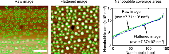
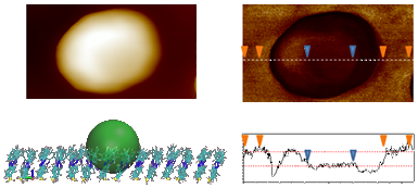
- points compared with the other two methods. As mentioned earlier, due to the finite size of AFM tips, the AFM images are actually the convolution of AFM tips with the real topography of samples. Here NB/ND characterization was implemented after tip correction (see Equations 1–3). Figure 12a and Figure


Increasing the stability of DNA nanostructure templates by atomic layer deposition of Al2O3 and its application in imprinting lithography
Beilstein J. Nanotechnol. 2017, 8, 2363–2375, doi:10.3762/bjnano.8.236
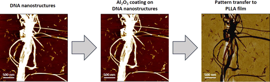
- individual AFM tips, which can give different measurements of the same sample. We attribute the decrease in the FWHM from the DNA nanotube master template to the PLLA stamp to the AFM probe convolution effect. These results confirm a faithful pattern transfer from the DNA nanotube master template to the PLLA



Colorimetric gas detection by the varying thickness of a thin film of ultrasmall PTSA-coated TiO2 nanoparticles on a Si substrate
Beilstein J. Nanotechnol. 2017, 8, 229–236, doi:10.3762/bjnano.8.25
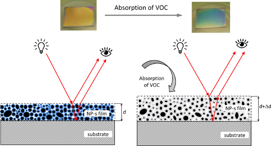
- mode was utilized in order to provide an optimal performance. OTESPA AFM tips (manufactured by Bruker) were used. To measure thickness of films, they were scratched with stainless steel tweezers and the step height of the scratch was measured. To ensure that only the film was scratched away (and not


Customized MFM probes with high lateral resolution
Beilstein J. Nanotechnol. 2016, 7, 1068–1074, doi:10.3762/bjnano.7.100
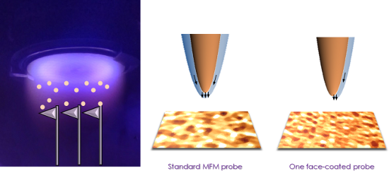
- broad range of samples, having a nominal Co layer of either 20 or 25 nm. Single crystalline silicon substrates were placed close to the AFM tips during deposition and used as reference samples for vibrating sample magnetometry (VSM) and AFM/MFM characterization. In all the experiments shown hereafter
- need to even further increase the lateral resolution. This could be achieved by reducing the thickness deposited onto the AFM tips at the expense of reducing their magnetic sensitivity. Figure 3 displays the topography and MFM image of a different region of the same hard disk obtained by a custom-made
- ]. Conclusion In this work we describe an accessible route for customizing MFM probes to desire by coating one side of standard AFM tips using sputtering. We demonstrate that the resulting probes achieve lateral resolutions at least as good as commercial super-sharp tips (10 nm and 25 nm in topographic and MFM


Assembling semiconducting molecules by covalent attachment to a lamellar crystalline polymer substrate
Beilstein J. Nanotechnol. 2016, 7, 784–798, doi:10.3762/bjnano.7.70
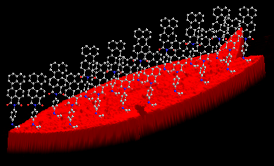
- varying in size. However, the exact habit cannot be determined due to limited resolution introduced by AFM tips having a radius of curvature of about 10 nm. The nanocrystals within the monolayer were found to be packed rather densely. However, there were voids between the nanocrystals, as they are hard
- images of the nanocrystals, AFM-tips with a nominal radius of curvature of 8 or 10 nm and a resonance frequency around 150 kHz or 320 kHz were used. Both had force constants of the cantilever of about 40 N/m. For the images of the functionalized/non-functionalized CPE45 crystals, sharp AFM tips with


Investigating organic multilayers by spectroscopic ellipsometry: specific and non-specific interactions of polyhistidine with NTA self-assembled monolayers
Beilstein J. Nanotechnol. 2016, 7, 544–553, doi:10.3762/bjnano.7.48
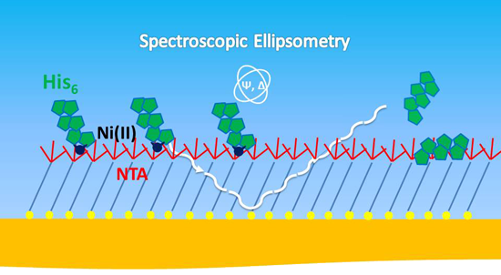
- using multi-chelator constructs [22][23] or double hexahistidine tags [24]. Among applications, the NTA–Ni(II)–His coupling has been exploited for the functionalization of nanoparticles [25][26][27] and atomic force microscopy (AFM) tips [28] as well as for more biologically oriented applications such
- mode with commercial AFM tips (NSC19 Mikromasch, k = 0.6 N/m), applying a high load (100 nN) in a confined (from 0.5 × 0.5 to 2 × 2 μm2) scanning area. The applied load is sufficient to displace the NTA molecules that are substituted by the T-OEG6 molecules present in the ethanol solution [65][66]. The



Length-extension resonator as a force sensor for high-resolution frequency-modulation atomic force microscopy in air
Beilstein J. Nanotechnol. 2016, 7, 432–438, doi:10.3762/bjnano.7.38
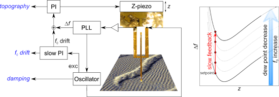
- separate feedback (constant-amplitude FM-AFM). Tips from commercial cantilevers (e.g., Olympus AC160-R3, Nanosensors SSS-NCH) are glued to the front face of the protruding oscillating beam with silver epoxy (E4110-LV, EPO-TEK Epoxy Technology). Environmental conditions are monitored with a digital


Rigid multipodal platforms for metal surfaces
Beilstein J. Nanotechnol. 2016, 7, 374–405, doi:10.3762/bjnano.7.34

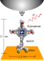
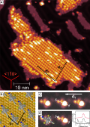
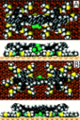
- showed that these macrocyclic trilactam moieties 12 terminated with 4-(acetylsulfanylmethyl)phenyl anchors are of sufficient size and rigidity to be visualized with a conventional AFM tip, as well as these well-defined bulk molecules may be further used for the calibration of AFM tips. Extended










A simple and efficient quasi 3-dimensional viscoelastic model and software for simulation of tapping-mode atomic force microscopy
Beilstein J. Nanotechnol. 2015, 6, 2233–2241, doi:10.3762/bjnano.6.229
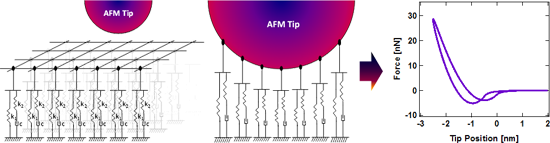
- use of an array of SLS elements leads to force curves that have the typical upward curvature in the repulsive region, while still offering a very low computational cost. Furthermore, the use of a multidimensional model allows for the study of AFM tips having non-ideal geometries, which can be
- symmetric AFM tips and surfaces, including a defective tip that has a cluster protruding from its apex (this is described below). Similarly, the software tool provided assumes radial symmetry, but it can be easily modified to allow deviations from it. Figure 4a shows a typical force curve for the Q3D model


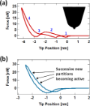

Kelvin probe force microscopy for local characterisation of active nanoelectronic devices
Beilstein J. Nanotechnol. 2015, 6, 2193–2206, doi:10.3762/bjnano.6.225
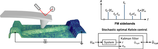
- optimise device performance, for example as field effect transistors. Figure 9b displays the simultaneously acquired C'', calculated from the 2ωm sideband amplitudes, Equation 14. To ensure highest lateral potential resolution, we used highly doped silicon AFM tips (Olympus AC160TS-R3) without a metal


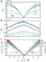
![[Graphic 33]](/bjnano/content/inline/2190-4286-6-225-i48.png?max-width=637&scale=1.18182) for different modulation amplitu...
for different modulation amplitu...




Development of a novel nanoindentation technique by utilizing a dual-probe AFM system
Beilstein J. Nanotechnol. 2015, 6, 2015–2027, doi:10.3762/bjnano.6.205
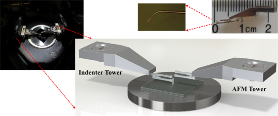
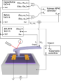
- and 20 nm tip radius, and they are mounted onto the lower tine of the tuning forks. An example image of cantilevered AFM tips is also shown in Figure 4. The material under investigation is placed on a flat sample holder on the lower piezo scanner. Initially, the left hand side probe (indenter tower


Mapping of elasticity and damping in an α + β titanium alloy through atomic force acoustic microscopy
Beilstein J. Nanotechnol. 2015, 6, 767–776, doi:10.3762/bjnano.6.79
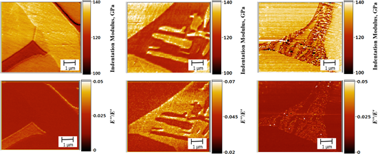
- moment of inertia. By using an appropriate contact mechanics model, one can convert the obtained stiffness values to the reduced elastic modulus E* and then to the indentation modulus M. The contact mechanics for AFM tips is very difficult to model as the exact shape of the tip in contact with the sample


Characterization of 10,12-pentacosadiynoic acid Langmuir–Blodgett monolayers and their use in metal–insulator–metal tunnel devices
Beilstein J. Nanotechnol. 2014, 5, 2240–2247, doi:10.3762/bjnano.5.233
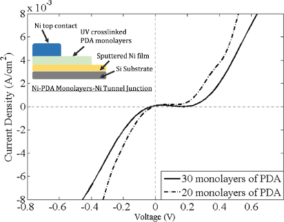
- case for a redox system. The roughness of the deposited monolayers was analyzed using atomic force microscopy (AFM) as shown in Figure 6. Special Bruker AFM tips (0.01–0.025 Ohm·cm, Sb-doped Si) were utilized to scan the film morphology. An average roughness, Ra, of 34.2 Å was measured for 30 layers of


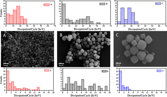
Exploring the retention properties of CaF2 nanoparticles as possible additives for dental care application with tapping-mode atomic force microscope in liquid
Beilstein J. Nanotechnol. 2014, 5, 36–43, doi:10.3762/bjnano.5.4
- related the demineralization and remineralization processes to softening of the enamel [23][24]. Another study recorded force–distance curves with AFM tips on etched superficial enamel substrate to examine the softening of enamel [25]. The formation of fluoride-containing nanostructures on tooth enamel


Growth behaviour and mechanical properties of PLL/HA multilayer films studied by AFM
Beilstein J. Nanotechnol. 2012, 3, 778–788, doi:10.3762/bjnano.3.87
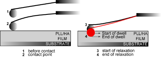
- tips, prevent errors due to insufficient indentation forces [15] and allow all scanning and force measurements to be done without changing any parameters [13][17][21]. On the other hand, shape and size determination of AFM tips is not straightforward, tips are more vulnerable to deformation during the
- the film’s mechanical properties and makes a comparison of different surfaces possible [23]. Therefore, a fixed indentation velocity of 400 nm/s was used for the elasticity measurements in the following section. Effect of film thickness and indenter size on Young’s modulus Small indenters, e.g., AFM


Effect of the tip state during qPlus noncontact atomic force microscopy of Si(100) at 5 K: Probing the probe
Beilstein J. Nanotechnol. 2012, 3, 25–32, doi:10.3762/bjnano.3.3
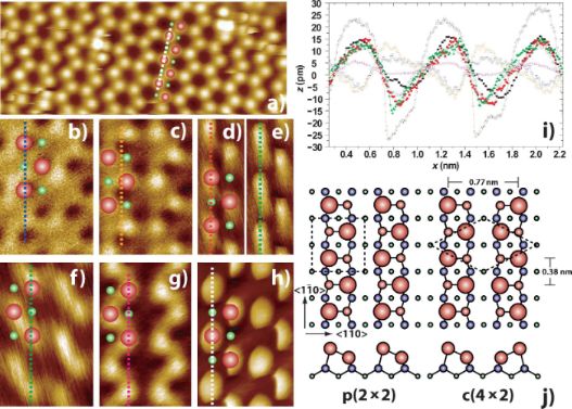
- access a wider apex parameter space than is available from conventionally prepared silicon cantilever AFM tips. Moreover, it must be noted that although we strongly suspect our tips are bulk silicon terminated, at least four atomic species (W and O from the tip and Si and B from the surface) are, in


Direct monitoring of opto-mechanical switching of self-assembled monolayer films containing the azobenzene group
Beilstein J. Nanotechnol. 2011, 2, 834–844, doi:10.3762/bjnano.2.93
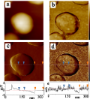
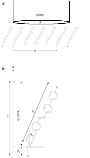
- thickness. However, this range can be significantly extended in the case of sharp AFM tips [17], and, for soft films on hard substrates, as much as half of the film thickness can be penetrated without experiencing appreciable substrate effects [18]. In any case, film deformation must be kept to a minimum



Manipulation of gold colloidal nanoparticles with atomic force microscopy in dynamic mode: influence of particle–substrate chemistry and morphology, and of operating conditions
Beilstein J. Nanotechnol. 2011, 2, 85–98, doi:10.3762/bjnano.2.10
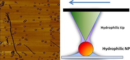
- microscopy techniques and quantitative information on interfacial friction was extracted from the lateral manipulation of these nanoparticles [17]. These particles were first pushed on a graphite surface by the AFM tips and then manipulated by placing the AFM tip on top of the particles. Above a certain


Switching adhesion forces by crossing the metal–insulator transition in Magnéli-type vanadium oxide crystals
Beilstein J. Nanotechnol. 2011, 2, 59–65, doi:10.3762/bjnano.2.8
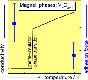
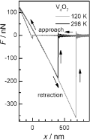
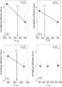
- between the cleavage planes of various vanadium oxide Magnéli phases (n = 3 … 7) and spherical titanium atomic force microscope (AFM) tips by systematic force–distance measurements with a variable-temperature AFM under ultrahigh vacuum conditions (UHV). The results show, for all investigated samples, that



Preparation and characterization of supported magnetic nanoparticles prepared by reverse micelles
Beilstein J. Nanotechnol. 2010, 1, 24–47, doi:10.3762/bjnano.1.5