Search results
Search for "silicon" in Full Text gives 913 result(s) in Beilstein Journal of Nanotechnology. Showing first 200.
Thickness dependent oxidation in CrCl3: a scanning X-ray photoemission and Kelvin probe microscopies study
Beilstein J. Nanotechnol. 2025, 16, 749–761, doi:10.3762/bjnano.16.58
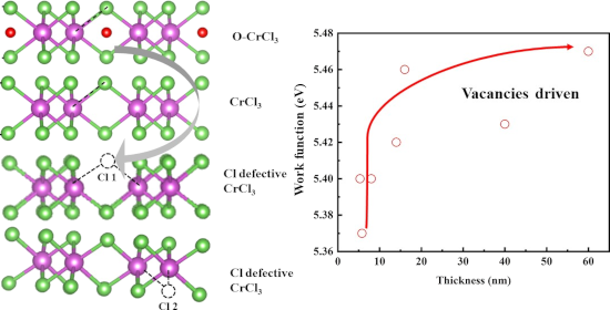
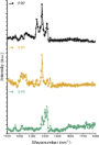
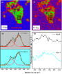
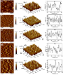
- , Faculty of Applied Physics and Mathematics, 80-233 Gdansk, Poland 10.3762/bjnano.16.58 Abstract The modifications in the electronic properties induced by the thickness and size of an individual flake of transition-metal halides on different substrates (silicon oxide or In-doped tin oxide) are of
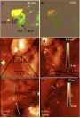
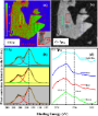
- silicon oxide substrate would help the determination of flakes thickness, we used also a more conductive substrate to measure photoemission under X-ray irradiation, that is, 1 nm thick native oxide Si substrates. Another convenient substrate for SPEM was 190 nm thick indium-doped tin oxide on glass





Synthesis of a multicomponent cellulose-based adsorbent for tetracycline removal from aquaculture water
Beilstein J. Nanotechnol. 2025, 16, 728–739, doi:10.3762/bjnano.16.56
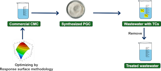
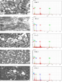
- Field-emission SEM analysis was performed using a Merlin Compact instrument (Carl Zeiss, Jena, Germany) with an SE2 detector. The sample was mounted on a clean silicon wafer and coated with a nanoscale platinum layer using an ion sputter coater (Q150T Plus, Quorum Technologies, UK). EDX analysis was


Colloidal few layered graphene–tannic acid preserves the biocompatibility of periodontal ligament cells
Beilstein J. Nanotechnol. 2025, 16, 664–677, doi:10.3762/bjnano.16.51
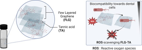
- pipetted onto clean silicon wafer substrates. The substrates were then air-dried and mounted on aluminum pins using double-sided carbon tape. Corresponding SEM images were subsequently captured. The S/TEM characterization was performed using a JEOL2100F microscope outfitted with a probe corrector for




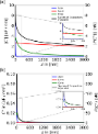
Nanoscale capacitance spectroscopy based on multifrequency electrostatic force microscopy
Beilstein J. Nanotechnol. 2025, 16, 637–651, doi:10.3762/bjnano.16.49

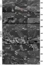
- variable-frequency detection of C′, we apply two AC voltages of the same magnitude (VAC,1 = VAC,2) at frequencies n and (n + 1) times the second resonance frequency ωm,2. According to Equation 10, this will excite an oscillation at ωm,2 with an amplitude proportional to C′. Silicon microcapacitors To
- nanospectroscopy experiments. The microcapacitors were produced by focused ion beam (FIB) milling on a silicon wafer with a 300 nm layer of SiO2 and a 14 nm sputtered layer of Pt on it (Figure 2). Results and Discussion To investigate whether the C″-sensitive detection leads to an improved spatial resolution of
- locations on the microcapacitor sample. The first spectrum was recorded on one of the microcapacitors (C3, see Figure 2). Then, we measured in one of the FIB-etched trenches around the capacitors. Here, we assume that the bare silicon surface is covered by a thin native oxide layer (Si). Last, we measured




Polyurethane/silk fibroin-based electrospun membranes for wound healing and skin substitute applications
Beilstein J. Nanotechnol. 2025, 16, 591–612, doi:10.3762/bjnano.16.46
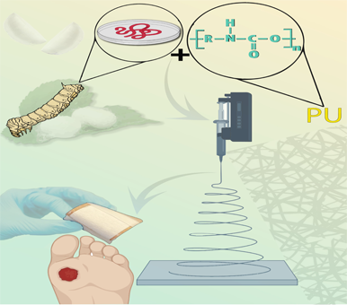
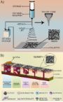
- to create and analyze SF films with various nanostructures that exhibit tunable optical properties depending on the structure. When combined with silicon photodiodes, the power conversion efficiency increased by 6.96% with flat SF films and 14.9% with nanopatterned SF films. This demonstrates the
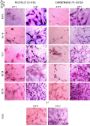
- design offers a large surface area. They are biocompatible, lowering the possibility of negative immune responses, and are adaptable to the use as films, gels, or scaffolds for different kinds of wounds [169]. Materials such as gold nanoparticles, graphene oxide, and silicon nanostructures are frequently



Retrieval of B1 phase from high-pressure B2 phase for CdO nanoparticles by electronic excitations in CdxZn1−xO composite thin films
Beilstein J. Nanotechnol. 2025, 16, 551–560, doi:10.3762/bjnano.16.43

- are predominantly attributed to the silicon substrate, with notable peaks at 303, 520, 620, and 671 cm−1. The peak at 435.9 cm−1 corresponds to the E2(H) mode characteristic of the wurtzite ZnO phase [17]. The persistence of the E2(high) mode across all O and Ag ion irradiated thin films, indicates
- temperature of 900 °C, Si diffusion intensifies, resulting in an increased thickness of the amorphous silicon oxide layer at the film–substrate interface [24]. The interdiffusion of Si, O, Cd, and Zn atoms near the SiOx layer (i.e., at the substrate–film interface) facilitates the formation of willemite


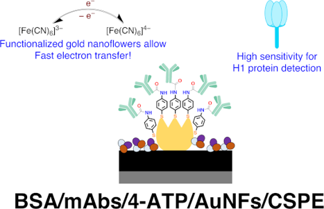
Functionalized gold nanoflowers on carbon screen-printed electrodes: an electrochemical platform for biosensing hemagglutinin protein of influenza A H1N1 virus
Beilstein J. Nanotechnol. 2025, 16, 540–550, doi:10.3762/bjnano.16.42
- sealed in place using silicon glue (Elastosil A07, Wacker). The device also consisted of two inlets and one outlet through which reagents can be made to pass through the device. The inlets and outlets were connected to reagent sources using silicon tubing (inner diameter = 1 mm, VWR). Preparation of the


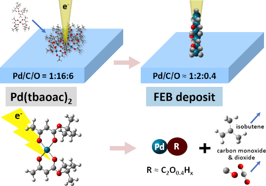
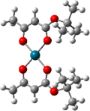
Electron beam-based direct writing of nanostructures using a palladium β-ketoesterate complex
Beilstein J. Nanotechnol. 2025, 16, 530–539, doi:10.3762/bjnano.16.41
- effective dwell time with a 600 nm FWHM of the electron beam), and 2000 cycles. For deposit morphology observation, a high-resolution Hitachi S4800 FESEM was used. The chemical composition of the deposits was confirmed through energy-dispersive X-ray spectroscopy (EDX) using a silicon drift detector from
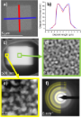
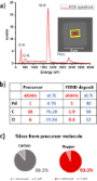
- of the thin focused electron beam (FEB) deposit containing Pd, C, and O without substrate interference (native silicon oxide and silicon), the SAMx Stratagem thin film correction software, based on the work by Pouchou and Pichoir [43] was employed. Stratagem needs k-ratios (i.e., the ratio of X-ray
- SEM microscope with the same temperatures and GIS positions as those employed for FEB depositions on native-oxide silicon substrates. A square area of 0.97 × 0.97 µm2 was deposited at 20 keV electron energy, with a dwell time of 500 ns and a point-to-pitch of 9.5 nm. The stage current was measured to


N2+-implantation-induced tailoring of structural, morphological, optical, and electrical characteristics of sputtered molybdenum thin films
Beilstein J. Nanotechnol. 2025, 16, 495–509, doi:10.3762/bjnano.16.38
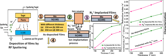
- minimizing the reflected power. Before deposition, the target surface was pre-sputtered for 15 min to remove any surface contamination. The silicon substrates were meticulously cleaned by washing them with distilled water and isopropyl alcohol and rinsing them with acetone. The vacuum chamber was evacuated


Performance optimization of a microwave-coupled plasma-based ultralow-energy ECR ion source for silicon nanostructuring
Beilstein J. Nanotechnol. 2025, 16, 484–494, doi:10.3762/bjnano.16.37

- extraction-based ion sources. Plasma physics principles are employed to interpret the observed variations in the beam current with various parameters. The optimized beam current is used to investigate the inert ion-induced nanopatterning of silicon surfaces, at various ion fluences and incidence angles. The
- beam current varies with different ion energies [29][30]. This article focuses on optimizing the beam current generated by a cost-effective microwave-based ECR ion source and the subsequent development of nanoscale patterns on the surface of silicon. The relationship between the beam current and
- various parameters is extensively examined and elucidated. Experimental parameters, spanning from plasma generation to ion beam extraction, are systematically optimized for the study of low-energy Ar-ion-induced nanostructures on silicon. The dependence of the extracted ion beam on gas pressure, magnetron


Synthetic-polymer-assisted antisense oligonucleotide delivery: targeted approaches for precision disease treatment
Beilstein J. Nanotechnol. 2025, 16, 435–463, doi:10.3762/bjnano.16.34


Size control of nanoparticles synthesized by pulsed laser ablation in liquids using donut-shaped beams
Beilstein J. Nanotechnol. 2025, 16, 407–417, doi:10.3762/bjnano.16.31
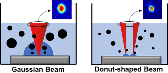
- and Figure 1c, respectively). To monitor the polarization of the donut-shaped beam, an additional Glan–Taylor polarizer was placed in front of the profiler. The spot diameters, 2wo, of the Gaussian beams (where wo is the beam waist) at the sample surface were measured with a silicon target using the
- D2 technique [51], obtaining similar spot sizes of 65 µm for the PHAROS laser and 72 µm for the NXT laser (1/e2 criterion). To evaluate the effective spot for the donut-shaped beam, we measured the pulse energy required to induce silicon damage and found that it is ca. 2.7 times higher than that for
- the morphology and size of the NPs synthesized by PLAL, the colloidal samples were drop-cast on a silicon wafer and dried for microscopic analysis. All NPs were characterized using scanning electron microscopy (SEM, Quanta 400 FEG, FEI Company, USA and TESCAN MIRA3 LMH, Brno, Czech Republic). The


Engineered PEG–PCL nanoparticles enable sensitive and selective detection of sodium dodecyl sulfate: a qualitative and quantitative analysis
Beilstein J. Nanotechnol. 2025, 16, 385–396, doi:10.3762/bjnano.16.29
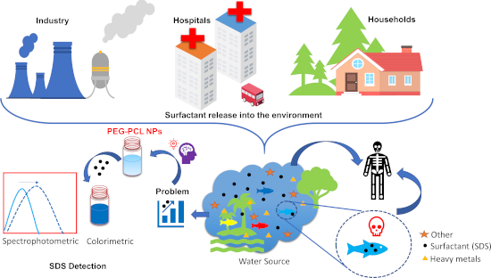
- as silicon oil (Cat. No. 015067), were obtained from CDH Fine Chemicals (India). All chemicals were used as received without further purification. Prior to experimentation, all glassware was cleaned with aqua regia (HCl:HNO3, 3:1 v/v) and thoroughly rinsed with double-distilled water. Methodology
- vigorously stirred in a silicon oil bath at 130 °C. Subsequently, a syringe introduced 2 mL of ε-caprolactone and 1 mL of stannous octoate (as a reaction catalyst) into the molten mPEG. The polymerization reaction was conducted under vacuum with continuous stirring at 130 °C for 24 h. After the


Pulsed laser in liquid grafting of gold nanoparticle–carbon support composites
Beilstein J. Nanotechnol. 2025, 16, 349–361, doi:10.3762/bjnano.16.26
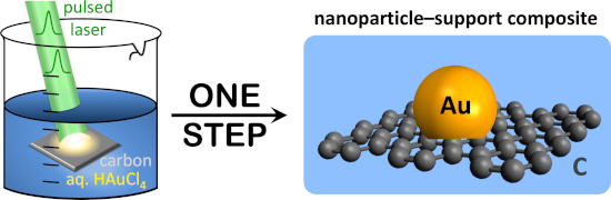
- scanning electron microscope with a Schottky field-emission emitter was operated at 20.00 kV with a working distance of 4.9 mm. Energy-dispersive X-ray (EDX) spectroscopy data were collected using an SEM-integrated EDAX Octane elect plus spectrometer with a with silicon drift detector. Double sided carbon


Tailoring of physical properties of RF-sputtered ZnTe films: role of substrate temperature
Beilstein J. Nanotechnol. 2025, 16, 333–348, doi:10.3762/bjnano.16.25
- fossil fuels to fulfil the growing demands of energy results in environmental pollution. Environmentally friendly resources such as solar and wind energy can act as a substitute for these non-renewable energy resources because of their sustainability and abundance. Commonly, silicon-based solar cells are
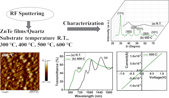
- substrate are two important parameters for substrate selection. To the best of our knowledge, studies related to the impact of the substrate (silicon and quartz) and film deposition temperature up to 600 °C on the structural, morphological, optical, and electrical behaviour of RF-sputtered ZnTe films are
- ZnTe films on silicon substrates [24]. It was observed that 400 °C is the optimum temperature for the growth of ZnTe films. In this study, our we focus on optimizing the deposition parameters for ZnTe films on quartz substrates and study the impact of substrate temperature (300–600 °C) on various




Correction: AFM-IR investigation of thin PECVD SiOx films on a polypropylene substrate in the surface-sensitive mode
Beilstein J. Nanotechnol. 2025, 16, 252–253, doi:10.3762/bjnano.16.19
- /bjnano.16.19 Keywords: AFM-IR; polypropylene; surface-sensitive mode; silicon oxide; thin films; XPS; The authors regret that the acknowledgement in the publication is unfortunately not complete. The following sentence in the Funding section is missing: This work was supported by the German Research
Advanced atomic force microscopy techniques V
Beilstein J. Nanotechnol. 2025, 16, 54–56, doi:10.3762/bjnano.16.6
- calculations. Eftekari et al. measure the local surface photovoltage generated in a silicon photodiode integrated with a piezoelectric membrane [8]. The design of such a device allows for the laterally resolved simultaneous quantification of the photovoltage generated by the photodiode as well as the
Theoretical study of the electronic and optical properties of a composite formed by the zeolite NaA and a magnetite cluster
Beilstein J. Nanotechnol. 2025, 16, 44–53, doi:10.3762/bjnano.16.5
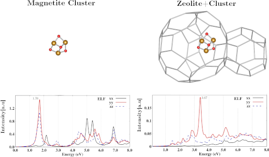
- , 1.60, 1.90, and 1.70 for aluminum, oxygen, silicon, sodium, and sulfur, respectively; the convergence number, that is, the smallest muffin-tin radii times the plane wave cutoff parameter, is set at RmtKmax = 6.0; the maximum l value for partial waves used inside atomic spheres is lmax = 10; and the




Bioinspired nanofilament coatings for scale reduction on steel
Beilstein J. Nanotechnol. 2025, 16, 25–34, doi:10.3762/bjnano.16.3

- surfaces. The elemental composition in Figure 4B shows the silicon emission expected for the SNF film, which is not present on the bare steel surface. Oxygen and carbon, additional components of the SNF coating, are also detected for the SNFs. At the same time, these elements are also observed on the bare


Orientation-dependent photonic bandgaps in gold-dust weevil scales and their titania bioreplicates
Beilstein J. Nanotechnol. 2025, 16, 1–10, doi:10.3762/bjnano.16.1
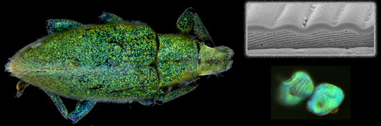
- in-lens secondary electron detector at 5 kV acceleration voltage. These samples were coated with gold using a Cressington 208 HR sputter coater. Elemental analysis was performed with 8 kV acceleration voltage, using an EDX detector attached to the Zeiss SEM (X-Max silicon drift energy-dispersive


Heterogeneous reactions in a HFCVD reactor: simulation using a 2D model
Beilstein J. Nanotechnol. 2024, 15, 1627–1638, doi:10.3762/bjnano.15.128
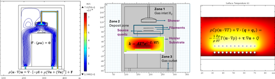
- for the subsequent growth of the SiOx films. These SiOx films have interesting properties and embedded nanostructures, which make them excellent dielectric, optoelectronic, and electroacoustic materials for the fabrication of devices compatible with silicon-based technology. Keywords: 2D model
- ; chemical reactions; flow dynamics; HFCVD; hot filament chemical vapor deposition; SiOx films; Introduction The growth of materials such as non-stoichiometric silicon oxide (SiOx) is an important step in semiconductor devices development. Control of deposition parameters determines the success of the
- process and the properties of the films, with the most important parameters being substrate temperature, gas pressure, species concentration, and flow velocity [1]. The structural, optical, and electrical properties of the SiOx, more generally known as silicon-rich oxide (SRO), films are determined by the


Facile synthesis of size-tunable L-carnosine-capped silver nanoparticles and their role in metal ion sensing and catalytic degradation of p-nitrophenol
Beilstein J. Nanotechnol. 2024, 15, 1576–1592, doi:10.3762/bjnano.15.124
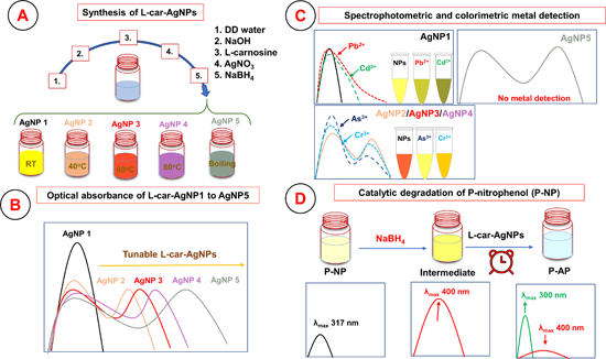
- edge filter using 532 nm as an excitation source. The Raman signal of the silicon wafer at 520 cm−1 was considered the reference point for spectrometer calibration, ensuring a spectral measurement accuracy better than 1 cm−1. The Raman spectra acquisition times were approximately 25 s for solid ʟ




Effect of radiation-induced vacancy saturation on the first-order phase transformation in nanoparticles: insights from a model
Beilstein J. Nanotechnol. 2024, 15, 1453–1472, doi:10.3762/bjnano.15.117

- comparison, in SiC, the energy of silicon vacancy migration is nearly 2.4 eV, and the energy of carbon vacancy migration is about 3.6 eV [42][43][44]. We focus on vacancy migration energies at the end of the paper and detail the findings. The surface energies σα and σβ of an iron-like nanoparticle are


Lithium niobate on insulator: an emerging nanophotonic crystal for optimized light control
Beilstein J. Nanotechnol. 2024, 15, 1415–1426, doi:10.3762/bjnano.15.114
- potential as a next-generation photovoltaic technology [41][42]. These cells offer a compelling alternative to traditional silicon solar cells because of the low manufacturing cost. Additionally, CQDs possess a unique property – their bandgap can be tuned by adjusting the size of the dots. This allows them
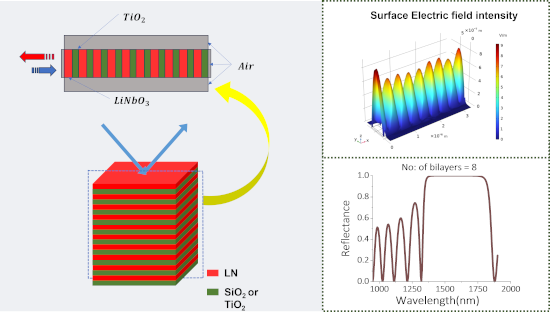
- telecommunications, sensing, and quantum optics applications, driving innovation in photonic technologies. We designed one-dimensional photonic crystals (1D PCs) made of lithium niobate with titanium dioxide and silicon dioxide using electromagenetic simulations. Our goal was to maximize reflectivity in the infrared


A biomimetic approach towards a universal slippery liquid infused surface coating
Beilstein J. Nanotechnol. 2024, 15, 1376–1389, doi:10.3762/bjnano.15.111
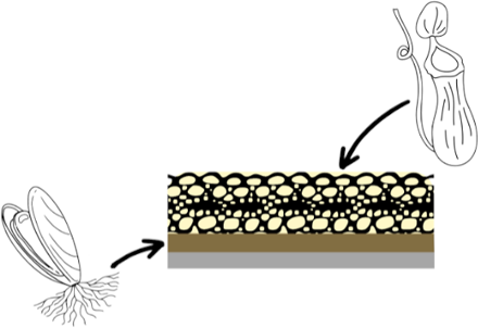
- cyclic olefin copolymer, silicon, and stainless steel substrates, by first growing a PDA film on each substrate. This was followed by a hydrophobic liquid anchor layer created by functionalizing the PDA film with a fluorinated thiol. Finally, perfluorodecalin was applied to the surface immediately prior
- copolymer (COC), silicon, and 316 stainless steel (SS) as our substrates. These substrates were first coated with PDA; then, a fluorinated thiol was attached to serve as the anchor for the infused fluid. The resulting surface modifications were then characterized by water contact angle measurements, atomic
- a 1:1 mixture of ethanol and acetone for 30 min. Si substrates were fabricated via a diamond-tipped blade in a Disco wafer saw (Disco, Tokyo, Japan) from a silicon wafer cut into 1 × 1 cm2 substrates. These Si substrates were left overnight to soak in DI water and then sonicated in 20 min intervals