Search results
Search for "scanning electron microscopy (SEM)" in Full Text gives 539 result(s) in Beilstein Journal of Nanotechnology. Showing first 200.
On the use of Raman spectroscopy to characterize mass-produced graphene nanoplatelets
Beilstein J. Nanotechnol. 2023, 14, 509–521, doi:10.3762/bjnano.14.42

- widely used characterization tool for GR2Ms [8]. A search of Web of Science showed that of 97,532 articles published in the last five years with “Graphene” in the abstract, 9.3% also mentioned “Raman”. This is compared with atomic force microscopy (AFM) (2.4%), scanning electron microscopy (SEM) (11.4


Mixed oxides with corundum-type structure obtained from recycling can seals as paint pigments: color stability
Beilstein J. Nanotechnol. 2023, 14, 467–477, doi:10.3762/bjnano.14.37

- results. The Raman modes are A1g (ca. 149 cm−1 and ca. 501 cm−1) and E1g (ca. 222 cm−1, ca. 290 cm−1, ca. 298 cm−1, ca. 402 cm−1, and ca. 615 cm−1, where 290 cm−1 and 298 cm−1 usually are a doublet with E1g symmetry and cannot be easily resolved [20]. Scanning electron microscopy (SEM) The morphology of


Evaluation of electrosynthesized reduced graphene oxide–Ni/Fe/Co-based (oxy)hydroxide catalysts towards the oxygen evolution reaction
Beilstein J. Nanotechnol. 2023, 14, 420–433, doi:10.3762/bjnano.14.34
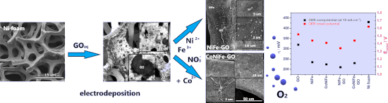
- the electrodeposition of conductive films on active metals [26]. The morphology of the deposits was analyzed by scanning electron microscopy (SEM) and is presented in Figure 1b–f. Typical GO flakes regularly distributed over the surface of the nickel foam were successfully obtained after the one-step


Biocatalytic synthesis and ordered self-assembly of silica nanoparticles via a silica-binding peptide
Beilstein J. Nanotechnol. 2023, 14, 280–290, doi:10.3762/bjnano.14.25

- scattering (DLS). The efficiency of the self-assembly was evaluated with scanning electron microscopy (SEM), UV–vis spectroscopy, and qualitative visual demonstration. Results and Discussion SiBP alone as catalyst Reaction kinetics were studied via OD measurements of the particles and GC analysis of


Batch preparation of nanofibers containing nanoparticles by an electrospinning device with multiple air inlets
Beilstein J. Nanotechnol. 2023, 14, 141–150, doi:10.3762/bjnano.14.15

- using an electronic balance (XJ120A, Precisa LTD.). The nanofiber morphology was investigated by a scanning electron microscopy (SEM, Hitachi S4800, Hitachi LTD.), and Image J software (National Institute of Mental Health) was used to characterize the fiber diameter distribution by random selection of


Antimicrobial and mechanical properties of functionalized textile by nanoarchitectured photoinduced Ag@polymer coating
Beilstein J. Nanotechnol. 2023, 14, 95–109, doi:10.3762/bjnano.14.11

- , as well as the final thickness of the metallic layer, account for this difference in reflectivity. Scanning electron microscopy (SEM) carried out on the surface of functionalized textiles revealed the homogenous distribution of AgNPs, with average sizes of 62 ± 2 nm and 58 ± 1 nm for the Ag@PEG600DA
- electron microscopy (SEM), transmission electron microscopy (TEM), and reflectance measurements to assess the optical properties and the durability of the functionalized textiles. Results and Discussion Photoinduced synthesis of the Ag@polymer coating Specific monomers poly(ethylene glycol) 600 diacrylate
- measurements. A Bio photometer UV–vis spectrometer from Eppendorf was used to assess bacteria and yeast suspensions by OD measurements at 600 nm. Surface characterizations were carried out using transmission electron microscopy (TEM) at 200 kV on a Philips CM200 instrument (LaB6 cathode) and scanning electron


Combining physical vapor deposition structuration with dealloying for the creation of a highly efficient SERS platform
Beilstein J. Nanotechnol. 2023, 14, 83–94, doi:10.3762/bjnano.14.10

- SERS properties of the nanoporous structure. Using scanning electron microscopy (SEM) and X-ray photoelectron spectroscopy (XPS) the morphology and surface composition of each nanoporous structure were respectively evaluated and used to describe the SERS properties of the samples. Results and


Orally administered docetaxel-loaded chitosan-decorated cationic PLGA nanoparticles for intestinal tumors: formulation, comprehensive in vitro characterization, and release kinetics
Beilstein J. Nanotechnol. 2022, 13, 1393–1407, doi:10.3762/bjnano.13.115

- characterization of both coated and uncoated DCX-PLGA NPs was carried out by scanning electron microscopy (SEM). As it can be seen in Figure 1, both formulations exhibit perfectly round spheres with smooth surfaces. No free DCX crystals were found in the SEM pictures of any formulation, confirming that DCX was


Enhanced electronic transport properties of Te roll-like nanostructures
Beilstein J. Nanotechnol. 2022, 13, 1284–1291, doi:10.3762/bjnano.13.106

- under mild conditions. A large quantity of these polycrystalline nanostructures with a diameter between 100 and 900 nm and a wall thickness around 50 nm were synthesized and characterized by scanning electron microscopy (SEM), energy dispersive X-ray spectroscopy (EDS), transmission electron microscopy
- reagents used were of analytic grade, purchased from Sigma-Aldrich Chemicals Company, and directly used without further purification. Morphology, elemental analysis, and crystal structure Morphology and elemental composition of the as-prepared products were characterized by scanning electron microscopy
- (SEM, FEI Quanta 3D FEG) at an acceleration voltage of 15.0 kV. An EDS system attached to the SEM was employed to analyze the chemical composition. TEM, high-resolution TEM (HRTEM) images, and SAED measurements were carried out in an FEI Tecnai G2-20 S-TWIN operated at 200 kV in a bright-field (BF) TEM


Studies of probe tip materials by atomic force microscopy: a review
Beilstein J. Nanotechnol. 2022, 13, 1256–1267, doi:10.3762/bjnano.13.104

- electric field. The nanotube tips produced by this method have strong adhesion and mechanical stability. Since the above methods require scanning electron microscopy (SEM) monitoring throughout the transfer process, the process is relatively time-consuming. Hafner et al. [40] proposed a new method to

Application of nanoarchitectonics in moist-electric generation
Beilstein J. Nanotechnol. 2022, 13, 1185–1200, doi:10.3762/bjnano.13.99

- in practical applications and provide green energy for more electronic devices. (a) The water flow is driven by an external electric field in the “motor” part, so the water molecules gain kinetic energy, and then an electromotive force is generated in the "Generator" part. (b) A scanning electron
- microscopy (SEM) image of an individual single-walled carbon nanotube (SWNT) device. (c) Dependence of the induced voltage difference, ΔV, on the quantity of water injected into the chamber. ΔV increases with the quantity of water inside the chamber and tends to saturate at 500 μL. It is nearly symmetric for


Rapid fabrication of MgO@g-C3N4 heterojunctions for photocatalytic nitric oxide removal
Beilstein J. Nanotechnol. 2022, 13, 1141–1154, doi:10.3762/bjnano.13.96

- properties of the materials. Scanning electron microscopy (SEM) and high-resolution transmission electron microscopy (HR-TEM) were used to assess the morphology of the materials. The crystal phase of the materials was determined by X-ray diffraction (XRD) with a measurement range of 10°–80°. Fourier


Biomimetic chitosan with biocomposite nanomaterials for bone tissue repair and regeneration
Beilstein J. Nanotechnol. 2022, 13, 1051–1067, doi:10.3762/bjnano.13.92

- -hydroxybutyrate) chitosan/multiwalled carbon nanotube scaffold coated with a nanobioglass–titania scaffold on bone cell regeneration was investigated. Scanning electron microscopy (SEM) examination verified the porosity of the scaffolds in the 300–700 µm range. The incorporation of chitosan into poly(3
Spindle-like MIL101(Fe) decorated with Bi2O3 nanoparticles for enhanced degradation of chlortetracycline under visible-light irradiation
Beilstein J. Nanotechnol. 2022, 13, 1038–1050, doi:10.3762/bjnano.13.91

- . Characterization of the as-prepared catalyst The crystalline structure of the prepared photocatalyst was analyzed by X-ray diffraction spectrometry (Empyrean, Panalytical, Holland) with Cu Kα radiation at a scanning speed of 7 °/min. The morphology of the samples was observed by scanning electron microscopy (SEM


Effects of focused electron beam irradiation parameters on direct nanostructure formation on Ag surfaces
Beilstein J. Nanotechnol. 2022, 13, 1004–1010, doi:10.3762/bjnano.13.87

- residual hydrocarbons by electron irradiation in scanning electron microscopy (SEM) vacuum chambers have been reported in several studies [12][13][14][15]. Hydrocarbon contamination from samples and vacuum pump oils is known to be ever present in vacuum chambers of electron microscopes [16][17][18]. The


Design of a biomimetic, small-scale artificial leaf surface for the study of environmental interactions
Beilstein J. Nanotechnol. 2022, 13, 944–957, doi:10.3762/bjnano.13.83

- morphologies of the wax on the upper (adaxial) and lower (abaxial) leaf sides (leaf 2, 3, and 4, n = 3) as well as of recrystallized wax structures on glass (n = 3) were analyzed by scanning electron microscopy (SEM, Gemini Supra 40 VP, Zeiss, Oberkochen, Germany). The middle part of fresh wheat leaves was cut
Micro-structures, nanomechanical properties and flight performance of three beetles with different folding ratios
Beilstein J. Nanotechnol. 2022, 13, 845–856, doi:10.3762/bjnano.13.75

- pasted flat on a slide for observation. Scanning electron microscopy (SEM) (Model EVO-18, Carl Zeiss Microimaging Inc., Germany) was used to obtain morphological images of cross sections of the hind wings of three beetles at the same locations of different wing veins. Nanoindentation properties The


A nonenzymatic reduced graphene oxide-based nanosensor for parathion
Beilstein J. Nanotechnol. 2022, 13, 730–744, doi:10.3762/bjnano.13.65

- phase of GO and RGO was characterized by X-ray diffraction (XRD) using a X’pertpro MPD XRD (PAN analytical B.V., the Netherlands) with Cu Kα radiation (λ = 1.5406 Å). Scanning electron microscopy (SEM) of the modified electrode was conducted on a JEOLEVO® 18 special edition (model: ZEISS EVO-MA 10) at


Reliable fabrication of transparent conducting films by cascade centrifugation and Langmuir–Blodgett deposition of electrochemically exfoliated graphene
Beilstein J. Nanotechnol. 2022, 13, 666–674, doi:10.3762/bjnano.13.58

- 10× (Olympus BX53M). Scanning electron microscopy (SEM) was performed with a FESEM (FEI Scios 2, Thermo Fisher Scientific, Waltham, MA, USA) at a chamber pressure of 1 × 10⁻⁴ Pa with electron beam voltages set between 1 and 30 kV, depending on the film. Films that are shown in optical dark-field


Antibacterial activity of a berberine nanoformulation
Beilstein J. Nanotechnol. 2022, 13, 641–652, doi:10.3762/bjnano.13.56

- solution were determined using Fourier-transform infrared spectroscopy (FTIR, NEXUS 670 from Nicolet). The FTIR analysis was conducted in transmission mode in the wavenumber range of 400 to 4000 cm−1. Size and shape of BBR NPs were investigated by scanning electron microscopy (SEM, S-4800, Hitachi) and


Sodium doping in brookite TiO2 enhances its photocatalytic activity
Beilstein J. Nanotechnol. 2022, 13, 599–609, doi:10.3762/bjnano.13.52

- , which is different from that observed via scanning electron microscopy (SEM) or transmission electron microscopy (TEM). Samples calcinated at 300–600 °C have a similar crystal size (ranging from 39–43 nm), suggesting that there is no obvious correlation between the crystal size and the photocatalytic


Design and characterization of polymeric microneedles containing extracts of Brazilian green propolis
Beilstein J. Nanotechnol. 2022, 13, 503–516, doi:10.3762/bjnano.13.42

- structure of microneedles containing glycolic extract of propolis (G1 to G9); magnification 40×. Arrows represent locations where bubbles are present. Micrographs obtained by scanning electron microscopy (SEM) showing the surface morphology microneedles containing ethanolic extract of propolis (E1 to E9
- ); magnification 150×. Micrograph obtained by scanning electron microscopy (SEM) showing the surface morphology of microneedles containing glycolic extract of propolis (G1 to G9); magnification 150×. Response surface plots for height and base measurements of MNs containing EE or GE. The color scale is indicated in


Ethosomal (−)-epigallocatechin-3-gallate as a novel approach to enhance antioxidant, anti-collagenase and anti-elastase effects
Beilstein J. Nanotechnol. 2022, 13, 491–502, doi:10.3762/bjnano.13.41

- characterized in vitro. Optimization of ETHs composed of 2–4% (w/v) of soya phosphatidylcholine (SPC) and 15–45% (v/v) of ethanol was performed based on characterization parameters (Table 1). The F3 formulation was chosen as the optimum one. A sample of F3 was examined by scanning electron microscopy (SEM


Investigation of electron-induced cross-linking of self-assembled monolayers by scanning tunneling microscopy
Beilstein J. Nanotechnol. 2022, 13, 462–471, doi:10.3762/bjnano.13.39

- structural changes is still lacking. In this work, we investigated the structural changes occurring upon irradiation of SAMs of p-terphenylthiol (TPT) on Au(111) using a combination of scanning electron microscopy (SEM) and scanning tunneling microscopy in ultrahigh vacuum (UHV) at room temperature. To study


Tubular glassy carbon microneedles with fullerene-like tips for biomedical applications
Beilstein J. Nanotechnol. 2022, 13, 455–461, doi:10.3762/bjnano.13.38

- pyrolysis of methane on a curved alumina surface. The surface provides the catalyst as well as the “strain” required to direct nucleation and growth. Figure 1a is a scanning electron microscopy (SEM) overview image showing a number of glassy carbon microneedles, which grow in the direction of the gas flow
- Raman spectroscopy (WiTec CRM200, laser excitation at 632.8 nm), scanning electron microscopy (SEM Leo 1530, with a spatial resolution of 1 nm at 20 kV and 3 nm at 1 kV, equipped with an energy-dispersive X-ray analysis system EDX INCA 400 from Oxford Instruments), and X-ray diffraction (STOE STADI-P


