Search results
Search for "nanostructure" in Full Text gives 366 result(s) in Beilstein Journal of Nanotechnology. Showing first 200.
Nonlinear absorption and scattering of a single plasmonic nanostructure characterized by x-scan technique
Beilstein J. Nanotechnol. 2019, 10, 2182–2191, doi:10.3762/bjnano.10.211

- simultaneous quantification for the nonlinear behavior of scattering, absorption and total attenuation by a single nanostructure. At low excitation intensities, both scattering and absorption responses are linear, thus confirming the linearity of the detection system. At high excitation intensities, we found
- nonlinearity of a single nanostructure, but also reports surprisingly large plasmonic nonlinearities. Keywords: absorption cross section; laser scanning microscopy; nanoplasmonics; nonlinear absorption; nonlinear scattering; single gold nanostructures; Introduction It is well known that the optical
- plasmonic nanostructures [4][5][6]. The potential applications of nonlinear nanoplasmonics include nanolasers [7], nanoantennas [8], surface plasmon polariton (SPP)-based waveguides [9], nanostructure-based optical limiters [10], nanoscopy instruments [11][12], and nanoelectronics as integrated optical


Review of advanced sensor devices employing nanoarchitectonics concepts
Beilstein J. Nanotechnol. 2019, 10, 2014–2030, doi:10.3762/bjnano.10.198

- nanoarchitectured motifs, such as nanoporous structures, ultrathin films, and unusual interfacial effects, for improved sensor performance is discussed. Most of the examples illustrate the crucial role of the nanostructure in sensor design. Although fine structural control used to be an important task in device


Pulsed laser synthesis of highly active Ag–Rh and Ag–Pt antenna–reactor-type plasmonic catalysts
Beilstein J. Nanotechnol. 2019, 10, 1958–1963, doi:10.3762/bjnano.10.192

- [1]. Plasmonic coupling results in an increase in the magnitude of the LSPR-induced electric fields. The selective adsorption of NP groupings to the Ag nanostructure concavities may be a result of LSPR-induced electric fields, which are largest in these highly angular regions. The mixed Ag–Pt colloid
- suspensions generated via pulsed laser ablation. Rh nanoparticle groupings were observed to only adsorb to Ag nanostructure concavities. Similar Ag–Pt heterostructures formed in the mixtures of colloidal Ag and Pt suspensions. UV–vis absorption spectra of the monometallic Ag, Pt, Rh, and the colloidal Ag–Rh


Fabrication and characterization of Si1−xGex nanocrystals in as-grown and annealed structures: a comparative study
Beilstein J. Nanotechnol. 2019, 10, 1873–1882, doi:10.3762/bjnano.10.182

- magnetron sputtering and thermal annealing. A TEM analysis discussed below will elaborate on the observed nanostructure. Figure 3 shows the X-ray reflectometry (XRR) plot for as-deposited and annealed MLs. An increase in the mass density of SiGe (3.55 to 4.17 g/cm3) with increased annealing temperature was


Chiral nanostructures self-assembled from nitrocinnamic amide amphiphiles: substituent and solvent effects
Beilstein J. Nanotechnol. 2019, 10, 1608–1617, doi:10.3762/bjnano.10.156

- aggregated into microspherical structures (Figure 7b), which was likely due to the nanostructure of the ethanol assembly. However, both DMF organogels and THF organogels consist of right-handed helical nanostructures (Figure 7c and 7d). We speculated that the opposite chirality in DMF and THF assemblies to
- molecular chirality of the three NCLG molecules was derived from the same source, i.e., ʟ-glutamic acid. At the same time, the variation in the substituted position also led to different gelation abilities. Additionally, it was demonstrated that the chirality of a nanostructure can also be regulated by


Kelvin probe force microscopy work function characterization of transition metal oxide crystals under ongoing reduction and oxidation
Beilstein J. Nanotechnol. 2019, 10, 1596–1607, doi:10.3762/bjnano.10.155

- understanding of the operation of nanostructure electrochemical sensors [48]. Thus, we have focused on the systematic approach of the influence of ambient air on the work function of TiO and SrTiO3(100). Figure 6a shows the topography and work function of representative TiO nanowire networks before and after


Graphynes: an alternative lightweight solution for shock protection
Beilstein J. Nanotechnol. 2019, 10, 1588–1595, doi:10.3762/bjnano.10.154

- efforts make the realization of entire monocrystalline GYs possible in foreseeable future. As an atomically thin 2D carbon nanostructure, its application in various fields is currently explored. For instance, the relatively large pore sizes in GY allows for a usage in desalination and water purification


Highly ordered mesoporous silica film nanocomposites containing gold nanoparticles for the catalytic reduction of 4-nitrophenol
Beilstein J. Nanotechnol. 2019, 10, 1368–1379, doi:10.3762/bjnano.10.135

- of mesoporous silica as a framework for growing AuNPs in the silicate nanochannels with higher ordered nanostructure. In particular, the amount of AuNPs in our AuNP–film catalyst was only 0.04 mg, indicating that it is a good catalyst even with such a small amount and with a simple method for the


Janus-micromotor-based on–off luminescence sensor for active TNT detection
Beilstein J. Nanotechnol. 2019, 10, 1324–1331, doi:10.3762/bjnano.10.131

- previously published procedure with several modifications [42]. After treatment with poly(acrylic acid) (PAA), the surface of the UCNPs were functionalized with 3-aminopropyltriethoxysilane (APTES) to introduce the amine group. The nanostructure and morphology of the synthesized UCNPs were investigated by


Synthesis and characterization of quaternary La(Sr)S–TaS2 misfit-layered nanotubes
Beilstein J. Nanotechnol. 2019, 10, 1112–1124, doi:10.3762/bjnano.10.111

- ]. Typically, these nanostructures are synthesized by means of high-temperature reactions that allow the formation of different metal sulfide nanotubes [4][5]. Another type of hollow nanostructure, inorganic fullerene-like structures (IFs), is the result of bending of a 2D layer of WS2 or any other 2D material
- along two directions, resulting in a closed-cage quasi-spherical nanostructure [6]. Once available in large quantities [7][8], different electrical devices based on single WS2 and MoS2 nanotubes could be realized, including high-performance field effect transistors (FETs) [9][10] and electromechanical


Revisiting semicontinuous silver films as surface-enhanced Raman spectroscopy substrates
Beilstein J. Nanotechnol. 2019, 10, 1048–1055, doi:10.3762/bjnano.10.105

- dielectric constant of the metal, surrounding dielectric, shape and size of the nanostructure, and its orientation with respect to the electric component of the electromagnetic field [1][2]. At resonance, the electric field near the surface of metallic nanostructures can be greatly enhanced and localized in


Correlation of surface-enhanced Raman scattering (SERS) with the surface density of gold nanoparticles: evaluation of the critical number of SERS tags for a detectable signal
Beilstein J. Nanotechnol. 2019, 10, 1016–1023, doi:10.3762/bjnano.10.102

- phenomena, the local electric field enhancement due to the surface plasmon resonance of the metal nanostructure (electromagnetic enhancement) and the charge transfer between the molecule and the metal substrate (chemical enhancement) [6][7][8]. In addition, given the generally low Raman scattering cross
- allows the generation of Raman scattering signals as intense as that of fluorescent compounds and, in fact, can be exploited for Raman labelling [13][14][15][16][17]. A SERS tag is typically composed of a plasmonic nanostructure capable of large electromagnetic field enhancement, coated with organic
- local field enhancement in a AuNT with structure reproducing the aggregate in Figure 1B. In particular, the SERS enhancement factor (GSERS) was obtained from the 4th power of the ratio between the local electric field, Eloc, in the proximity to the surface of the metal nanostructure and the incident


In situ AFM visualization of Li–O2 battery discharge products during redox cycling in an atmospherically controlled sample cell
Beilstein J. Nanotechnol. 2019, 10, 930–940, doi:10.3762/bjnano.10.94

- different discharge capacities. These images reveal that the toroids have a fine nanostructure, as measured previously [39]. The end radius of the AFM tip, estimated to be between 5 nm and 10 nm, limits the image resolution. Motivated by our measurements of increased capacity at ≈2500 ppm water, the water
- contains <20 ppm water, the surface is not fully covered by nanostructure growth. This is reflected in lower recharge voltages for the electrolyte containing <20 ppm of water. Thus, our initial AFM observations support the hypothesis that during cell discharge, the presence of water increases superoxide
- surface. 3D volume analysis of electrochemical deposits formed on the glassy carbon surface in Figure 4. The red inset shows a 3D view of the surface at ≈12% discharge capacity. The nanostructures deposited on the surface exhibit platelet morphology. An even finer nanostructure was observed beyond the


Tungsten disulfide-based nanocomposites for photothermal therapy
Beilstein J. Nanotechnol. 2019, 10, 811–822, doi:10.3762/bjnano.10.81

- mediated by nanomaterials is less invasive than laser irradiation alone, requires lower radiation intensity, and its selectivity towards the tumor can be adjusted by carefully engineering the light-responsive nanostructure. In general, nanomaterials in the size range of 100–200 nm should give the maximum
- accumulation effect, but parameters such as nanostructure shape and surface charge are extremely important [33]. A wide range of nanomaterials has been studied for cancer PTT to now, from organic conjugated polymers [34][35], through carbon-based nanomaterials [36][37], to inorganic nanostructures. Within the


Renewable energy conversion using nano- and microstructured materials
Beilstein J. Nanotechnol. 2019, 10, 771–773, doi:10.3762/bjnano.10.76

- however be desired as the example of Co3O4 photocathodes in [7] shows. In general, the nanostructure of any material will strongly affect the corresponding optical and electronic properties by controlling the surface-to-volume ratio and the related morphological characteristics. Besides the concepts for
Features and advantages of flexible silicon nanowires for SERS applications
Beilstein J. Nanotechnol. 2019, 10, 725–734, doi:10.3762/bjnano.10.72

- flexible silicon nanowires (SiNWs) substrates for surface-enhanced Raman spectroscopy (SERS) applications. The novel SERS substrates are described in detail considering three main aspects. First, the key synthesis parameters for the flexible nanostructure SERS substrates were optimized. It is shown that


Biomimetic synthesis of Ag-coated glasswing butterfly arrays as ultra-sensitive SERS substrates for efficient trace detection of pesticides
Beilstein J. Nanotechnol. 2019, 10, 578–588, doi:10.3762/bjnano.10.59

- hybrids (Ag-G.b.) by magnetron sputtering technology. The 3D surface-enhanced Raman scattering (SERS) substrate is fabricated from an original chitin-based nanostructure, which serves as a bio-scaffold for Ag nanofilms to be coated on. The novel crisscrossing plate-like nanostructures of 3D Ag-G.b
- 101 to 102 [6]. Therefore, in order to achieve high EF with outstanding sensitivity as well as reproducibility, the best strategy is to design optimal nanostructure that maximizes the LSPR effect. According to previous reports [7][8], the lack of the SERS-active substrates with large-scale and high
- previous reports [29][30]. We adopt a highly efficient route (as shown in Figure 1) using biomimetic synthesis to fabricate 3D Ag nanofilm/glasswing butterfly wing (Ag-G.b.) hybrids as SERS substrates. The wings of the glasswing butterfly (Haetera piera) have an interesting nanostructure that can serve as


Hydrophilicity and carbon chain length effects on the gas sensing properties of chemoresistive, self-assembled monolayer carbon nanotube sensors
Beilstein J. Nanotechnol. 2019, 10, 565–577, doi:10.3762/bjnano.10.58

- ); self-assembled monolayer (SAM); thiol; Introduction Carbon nanotubes were first observed by Sumio Iijima in 1991 [1] and since then, this nanostructure has been widely used in chemoresistive gas sensors [2][3][4][5] due to the possibility to engineer its sensitivity towards chemicals present in a


Quantification and coupling of the electromagnetic and chemical contributions in surface-enhanced Raman scattering
Beilstein J. Nanotechnol. 2019, 10, 549–556, doi:10.3762/bjnano.10.56

- excitation, see Supporting Information File 1). (a) Liquid benzenthiol, (b) Au film, (c) Ag film, (d) Ag grating, and (e) Ag nanostructure. (f–j) Corresponding intensity ratios of the ω2 and ω3 modes normalized to the ω1 modes for both 633 nm and 785 nm excitation. Each data set is the average from


Widening of the electroactivity potential range by composite formation – capacitive properties of TiO2/BiVO4/PEDOT:PSS electrodes in contact with an aqueous electrolyte
Beilstein J. Nanotechnol. 2019, 10, 483–493, doi:10.3762/bjnano.10.49

- nanotubular morphology of TiO2 was obtained by Ti plate anodization. The nanostructure of TiO2 provides a high specific surface area that is crucial for energy storage devices based on pseudocapacitance and electrochemical double-layer capacitance. TiO2 nanotubes were covered by a nanometric layer of bismuth


Advanced scanning probe lithography using anatase-to-rutile transition to create localized TiO2 nanorods
Beilstein J. Nanotechnol. 2019, 10, 412–418, doi:10.3762/bjnano.10.40

- nanostructures. Keywords: hydrothermal crystal growth; lithography; nanostructures; seed crystals; surface processes; oxides; Introduction Rutile TiO2 is a chemically stable semiconductor with a band gap of 3.1 eV [1]. Dependent on the kind of nanostructure and doping, it has outstanding electronic and


Integration of LaMnO3+δ films on platinized silicon substrates for resistive switching applications by PI-MOCVD
Beilstein J. Nanotechnol. 2019, 10, 389–398, doi:10.3762/bjnano.10.38

- nanostructure growth was further analyzed in cross section by transmission electron microscopy (TEM), a JEOL 2011 equipment operating at 200 kV with a 0.19 nm point-to-point resolution. X-ray absorption near-edge spectroscopy (XANES) spectra at the Mn K-edge of LMO thin films were collected at the ESRF ID12


Geometrical optimisation of core–shell nanowire arrays for enhanced absorption in thin crystalline silicon heterojunction solar cells
Beilstein J. Nanotechnol. 2019, 10, 322–331, doi:10.3762/bjnano.10.31

- = 450 nm) can be mainly explained by a better in-coupling of light, promoted by the nanostructure array at the front side. Lower parasitic absorption at the front side can also explain the improvement. This results in a net gain in photocurrent density of 0.30 mAcm−2. At longer wavelengths, scattering
- introduced to improve the reflectivity of the contact. The flat reference employs the same layers (material and thickness) as the nanowire model, the only difference being the absence of the nanostructure array. In Figure 4, the calculated absorption in the c-Si layer (Ac−Si) is depicted, for both nanowire


Relation between thickness, crystallite size and magnetoresistance of nanostructured La1−xSrxMnyO3±δ films for magnetic field sensors
Beilstein J. Nanotechnol. 2019, 10, 256–261, doi:10.3762/bjnano.10.24

- ) phenomenon [1]. The complex physics of manganite materials provides an opportunity to tune their electric and magnetic properties over a wide range by variation of chemical composition [2][3][4][5], film thickness [6][7] and nanostructure [8][9], as well as induced lattice strain [10][11][12]. The manganite
- practical applications due to low sensitivity and large magnetic anisotropy [15][16]. For this reason, the investigation and control of the magnetoresistive properties of manganite materials on the nanometer scale is of great importance. It was shown that the change of nanostructure by variation of


Magnetic-field sensor with self-reference characteristic based on a magnetic fluid and independent plasmonic dual resonances
Beilstein J. Nanotechnol. 2019, 10, 247–255, doi:10.3762/bjnano.10.23
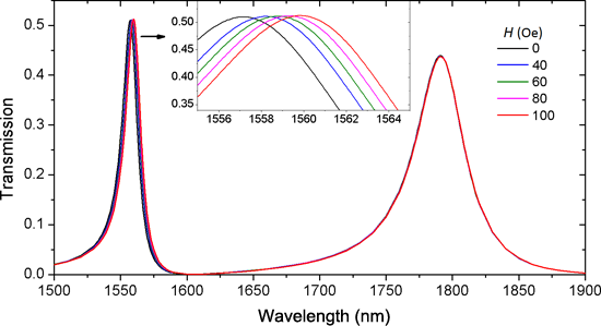
- accuracy. A simple and compact self-reference sensor with high sensitivity is achieved and it is promising in the integrated sensing and detection of magnetic fields. Methods The proposed plasmonic nanostructure is schematically shown in Figure 1. Two stubs are located on each side of the MDM waveguide. A


