Search results
Search for "SPM" in Full Text gives 95 result(s) in Beilstein Journal of Nanotechnology.
Triptycene-terminated thiolate and selenolate monolayers on Au(111)
Beilstein J. Nanotechnol. 2017, 8, 892–905, doi:10.3762/bjnano.8.91

- ]. Other methods with sufficient height resolutions (0.1 nm) are ellipsometry and scanning probe microscopy (SPM). To our knowledge, SPM methods have so far not been successfully used to determine the absolute thickness of organic self-assmbled monolayers, most likely due to difficulties with preparing a


Relationships between chemical structure, mechanical properties and materials processing in nanopatterned organosilicate fins
Beilstein J. Nanotechnol. 2017, 8, 863–871, doi:10.3762/bjnano.8.88

- scanning probe microscopy (SPM) [15][16][17][18][19][20][21]). It is due to the non-existence of techniques to identify chemical structures with nanometer lateral (in-plane) resolution. Scatterometry and near-field optical microscopy (NSOM) techniques have allowed sub-wavelength features to be resolved [22
- atomic force microscopy (AFM) and exploiting either near-field optical enhancements produced by the probe tip [25][26], or using the AFM probe to detect various photoinduced thermo-mechanical responses [24][27]. However, these techniques have yet to be routinely combined with other nanoscale SPM


Measuring adhesion on rough surfaces using atomic force microscopy with a liquid probe
Beilstein J. Nanotechnol. 2017, 8, 813–825, doi:10.3762/bjnano.8.84

- ., Russia) intended for 3D visualization of scanning tips (Figure 1). The grating with the sharp peaks was inspected with standard Si3N4 SPM cantilevers in contact mode. The scans were obtained with a scanning probe microscope in vacuum (1 × 10⁻⁴ Pa). The inverted images of the tip (not presented in this


Analysis and modification of defective surface aggregates on PCDTBT:PCBM solar cell blends using combined Kelvin probe, conductive and bimodal atomic force microscopy
Beilstein J. Nanotechnol. 2017, 8, 579–589, doi:10.3762/bjnano.8.62

- compositional variation occurs in the entire volume of the active layer. However, since SPM methods primarily characterize the surface (with or without tip–sample contact), we conclude that the ultra-thin layers investigated in this report rest on the surface. We also point out that the samples used here are


Copper atomic-scale transistors
Beilstein J. Nanotechnol. 2017, 8, 530–538, doi:10.3762/bjnano.8.57

- copper atomic-scale point contacts have been fabricated as mechanically controllable break junctions (MCBJ) [42][43][44][45], by using scanning probe microscopy (SPM) with a conductive tip [46][47], or electrochemical techniques [24][25][26][48][49]. Copper is an interconnection material in ultra-large


Noise in NC-AFM measurements with significant tip–sample interaction
Beilstein J. Nanotechnol. 2016, 7, 1885–1904, doi:10.3762/bjnano.7.181
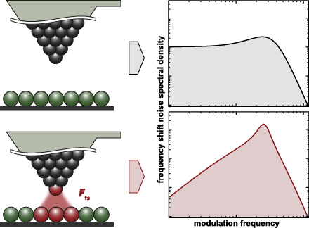
- Technology, Inc., Troy, MI, USA) operated at room temperature and employing the beam-deflection method to measure the cantilever displacement. Tip positioning and approach is accomplished by the SPM 100 control system (RHK Technology, Inc.). For this and all other instruments we introduce scaling factors to


![[Graphic 32]](/bjnano/content/inline/2190-4286-7-181-i73.png?max-width=637&scale=1.18182) wit...
wit...

![[Graphic 34]](/bjnano/content/inline/2190-4286-7-181-i75.png?max-width=637&scale=1.18182) wit...
wit...


Noncontact atomic force microscopy III
Beilstein J. Nanotechnol. 2016, 7, 946–947, doi:10.3762/bjnano.7.86

- particular, latest instrumental advances are highlighted in the form of a new design for a large-area SPM used for electrostatic force measurements, improvement of dynamic cantilever response by the utilization of reflective coatings and photothermal conversion layers, and the use of length extension
Rigid multipodal platforms for metal surfaces
Beilstein J. Nanotechnol. 2016, 7, 374–405, doi:10.3762/bjnano.7.34


Controlled graphene oxide assembly on silver nanocube monolayers for SERS detection: dependence on nanocube packing procedure
Beilstein J. Nanotechnol. 2016, 7, 9–21, doi:10.3762/bjnano.7.2

- rendering was performed using Gwyddion 2.30 SPM data visualization tool (http://gwyddion.net/). UV–vis measurements. UV–vis spectra of the nanocube suspension in ethanol and of monolayers deposited on quartz substrates were recorded using a Jasco V-6 UV–vis–NIR spectrophotometer with 1 nm slit and 200 nm


Large area scanning probe microscope in ultra-high vacuum demonstrated for electrostatic force measurements on high-voltage devices
Beilstein J. Nanotechnol. 2015, 6, 2485–2497, doi:10.3762/bjnano.6.258

- voltage; Introduction Scanning probe microscopy (SPM) is nowadays an established technological approach for surface analysis in many different research fields. Applications can be found in areas of life science measuring the properties of cells in buffer solution, submolecular structure of single
- proposed, successfully demonstrated, and found their way into commercially available SPM systems. However, the unperturbed measurements and the interpretation of the acquired data remains the most challenging task which requires a sophisticated fundamental interpretation. In recent years, especially the
- detection of electrostatic forces and the determination of local work function values was intensively discussed and models combining large scale influences with atomistic simulations have been developed [1][2][3][4]. As early as in the late 1980s H. Wickramasinghe proposed several SPM based methods for the


Virtual reality visual feedback for hand-controlled scanning probe microscopy manipulation of single molecules
Beilstein J. Nanotechnol. 2015, 6, 2148–2153, doi:10.3762/bjnano.6.220

- .6.220 Abstract Controlled manipulation of single molecules is an important step towards the fabrication of single molecule devices and nanoscale molecular machines. Currently, scanning probe microscopy (SPM) is the only technique that facilitates direct imaging and manipulations of nanometer-sized
- position of the SPM tip during manipulation in real time, while simultaneously plotting the experimentally measured frequency shift (Δf) of the non-contact atomic force microscope (NC-AFM) tuning fork sensor as well as the magnitude of the electric current (I) flowing between the tip and the surface. The
- (PTCDA); scanning probe microscopy (SPM); scanning tunnelling microscopy (STM); single-molecule manipulation; virtual reality interface; Introduction The recently introduced scanning probe microscopy (SPM) technique of hand controlled manipulation (HCM) allows the operator of the SPM to manipulate


Development of a novel nanoindentation technique by utilizing a dual-probe AFM system
Beilstein J. Nanotechnol. 2015, 6, 2015–2027, doi:10.3762/bjnano.6.205

- nanoindentation is described that exhibits improved resolution and depth sensing. The approach is based on a multi-probe scanning probe microscopy (SPM) tool that utilizes tuning-fork based probes for both indentation and depth sensing. Unlike nanoindentation experiments performed with conventional AFM systems
- nanoindentation. Zhao et al. present a nanoindentation device that is designed to operate inside an SEM chamber in order to perform in situ indentation tests of indium phosphide [14]. We report a novel approach using a multi-probe scanning probe microscopy (SPM) system with tuning-fork probe technology in an
- parameters that have been used for the rest of the experimental results. Overview of the novel multi-probe nanoindentation system The proposed system uses a multi-probe SPM instrument (Nanonics MultiView-4000) based on normal force tuning fork technology. The tuning forks have a resonance frequency of


Atomic scale interface design and characterisation
Beilstein J. Nanotechnol. 2015, 6, 1708–1711, doi:10.3762/bjnano.6.174
- density-functional theory (DFT) approaches. In addition, using DFT-based molecular dynamics, the manipulation of nanostructures by SPM tools and the changes made to the system by the characterization tools, e.g., the production of defects under electron irradiation and their evolution over time, can be
Scalable, high performance, enzymatic cathodes based on nanoimprint lithography
Beilstein J. Nanotechnol. 2015, 6, 1377–1384, doi:10.3762/bjnano.6.142

- SPM with a Nanoscope V control unit from Bruker AXS (Santa Barbara, CA, USA). The AFM was operated in the ScanAsyst mode. All images were obtained in air and at room temperature. Triangular silicon nitride cantilevers with a nominal spring constant of 0.4 N·m−1 (ScanAsyst Air probes, Bruker AXS) were


Electrical characterization of single molecule and Langmuir–Blodgett monomolecular films of a pyridine-terminated oligo(phenylene-ethynylene) derivative
Beilstein J. Nanotechnol. 2015, 6, 1145–1157, doi:10.3762/bjnano.6.116

- QCM measurements were carried out using a Stanford Research System instrument and employing AT-cut, α-quartz crystals with a resonance frequency of 5 MHz having circular gold electrodes patterned on both sides. An Agilent 5500 SPM microscope was used for characterization of the electrical properties


High sensitivity and high resolution element 3D analysis by a combined SIMS–SPM instrument
Beilstein J. Nanotechnol. 2015, 6, 1091–1099, doi:10.3762/bjnano.6.110

- Yves Fleming Tom Wirtz Advanced Instrumentation for Ion Nano-Analytics (AINA), MRT Department, Luxembourg Institute of Science and Technology (LIST), 41 rue du Brill, L-4422 Belvaux, Luxembourg 10.3762/bjnano.6.110 Abstract Using the recently developed SIMS–SPM prototype, secondary ion mass
- spectrometry (SIMS) data was combined with topographical data from the scanning probe microscopy (SPM) module for five test structures in order to obtain accurate chemical 3D maps: a polystyrene/polyvinylpyrrolidone (PS/PVP) polymer blend, a nickel-based super-alloy, a titanium carbonitride-based cermet, a
- of the TiCN cermet. Keywords: alloy; atomic force microscopy (AFM); correlative microscopy; differential sputtering; in situ; multimodal imaging; nano-cluster; polymer blend; secondary ion mass spectrometry (SIMS); scanning probe microscopy (SPM); SIMS artefacts; sputter-induced effects; sputter


Kelvin probe force microscopy in liquid using electrochemical force microscopy
Beilstein J. Nanotechnol. 2015, 6, 201–214, doi:10.3762/bjnano.6.19

- level, few techniques are capable of operating below the micron length scale [11]. Scanning probe microscopy (SPM) techniques are uniquely positioned to probe structure on nano- to micrometer length scales and can do so under vacuum, ambient or liquid environments. Thus, the development of SPM
- techniques that are capable of obtaining both structural information and information on local electrochemical functionality is a natural combination of capability and necessity [12][13][14][15]. In the past few decades, a plethora of SPM techniques capable of probing electrostatic, [16][17] electromechanical
- [18], electrochemical [19] and ionic [15] functionality on the nanoscale have been developed. A paradigmatic example of such development is closed loop-Kelvin probe force microscopy (KPFM) [20], which has become a widely used voltage-modulated SPM technique for the measurement of surface potential


![[Graphic 6]](/bjnano/content/inline/2190-4286-6-19-i11.png?max-width=637&scale=1.18182) response collected 200 nm above a grounded Au electrode in (a, b, c) air, (d, e, f) decane an...
response collected 200 nm above a grounded Au electrode in (a, b, c) air, (d, e, f) decane an...


![[Graphic 22]](/bjnano/content/inline/2190-4286-6-19-i27.png?max-width=637&scale=1.18182) spectra [bias-on] collected 500 nm above HOPG in aqueous solutions of increasing salt concent...
spectra [bias-on] collected 500 nm above HOPG in aqueous solutions of increasing salt concent...

![[Graphic 25]](/bjnano/content/inline/2190-4286-6-19-i30.png?max-width=637&scale=1.18182) spectra [bias-on] collected 500 nm above (a) HOPG and (b) Au in milli-Q water (vertical color...
spectra [bias-on] collected 500 nm above (a) HOPG and (b) Au in milli-Q water (vertical color...

![[Graphic 27]](/bjnano/content/inline/2190-4286-6-19-i32.png?max-width=637&scale=1.18182) spectra [bias-on] recorded 500 nm above a HOPG/Au boundary in milli-Q water. T...
spectra [bias-on] recorded 500 nm above a HOPG/Au boundary in milli-Q water. T...

Functionalization of α-synuclein fibrils
Beilstein J. Nanotechnol. 2015, 6, 124–133, doi:10.3762/bjnano.6.12

- the standard contact and tapping AFM modes by scanning probe microscope SPM D3100/Nanoscope IVa (Veeco, now Bruker). Two types of silicon tips, OTESPA and SNL (Bruker), were used. The images were processed by the Scanning Probe Image Processor, Version 5.1.0 software (Image Metrology, Denmark). The


Morphology, structural properties and reducibility of size-selected CeO2−x nanoparticle films
Beilstein J. Nanotechnol. 2015, 6, 60–67, doi:10.3762/bjnano.6.7

- 0.19 nm. The images were subsequently elaborated by using the STEM_CELL software [19]. Concerning the ultra-thin films we evaluated the morphology with in situ STM measurements by using an OMICRON room temperature SPM. The STM images have been processed by using the Image SXM software [20]. A second


Advanced atomic force microscopy techniques II
Beilstein J. Nanotechnol. 2014, 5, 2326–2327, doi:10.3762/bjnano.5.241
- surface reconstructions and nanoscale geometries. New functionality is achieved by combinations of nanoscale materials or by structuring their surfaces. The unrivaled tools for measurements of all kind of nanoscale properties are scanning probe microscopy (SPM) techniques, which were triggered by the
- the integration of various SPM techniques into biological and chemical experiments. The second volume of the Thematic Series “Advanced atomic force microscopy techniques”, which is presented here, compiles again exciting developments in nanoscale research based on SPM techniques addressed by the
- PTCDA islands [12]. Furthermore, the analysis of mechanical properties of either nanoparticles [13] or biological systems [14][15][16] is covered by several articles and reviewed by Cohen and co-workers [17]. Especially the application of advanced SPM techniques in biology provides exciting new results
Nanobioarchitectures based on chlorophyll photopigment, artificial lipid bilayers and carbon nanotubes
Beilstein J. Nanotechnol. 2014, 5, 2316–2325, doi:10.3762/bjnano.5.240

- diameters (based on the Stokes–Einstein equation) and the polydispersity index (PDI, indicating the width of the size distribution) were obtained from 3 individual measurements using an intensity distribution. Atomic force microscopy (AFM) AFM images were recorded on an integrated platform, AFM/SPM (NTEGRA


Patterning a hydrogen-bonded molecular monolayer with a hand-controlled scanning probe microscope
Beilstein J. Nanotechnol. 2014, 5, 1926–1932, doi:10.3762/bjnano.5.203

- molecular-scale functional design, which includes arranging molecules into complex structures at will. The first steps towards this goal were made through the invention of the scanning probe microscope (SPM), which put single-atom and single-molecule manipulation into practice for the first time. Extending
- the controlled manipulation to larger molecules is expected to multiply the potential of engineered nanostructures. Here we report an enhancement of the SPM technique that makes the manipulation of large molecular adsorbates much more effective. By using a commercial motion tracking system, we couple
- the movements of an operator's hand to the sub-angstrom precise positioning of an SPM tip. Literally moving the tip by hand we write a nanoscale structure in a monolayer of large molecules, thereby showing that our method allows for the successful execution of complex manipulation protocols even when


Dry friction of microstructured polymer surfaces inspired by snake skin
Beilstein J. Nanotechnol. 2014, 5, 1091–1103, doi:10.3762/bjnano.5.122

- . Scans were carried out at a 1 Hz scan rate and a resolution of 1024 × 1024 pixels with an intermittent contact mode cantilever (c = 50 N·m−1, NST-NCHF, Nascatec GmbH, Stuttgart, Germany), at ambient conditions (room temperature 24° C, relative humidity 41%). NanoWizard® SPM software 3.3.23 (JPK


A nanometric cushion for enhancing scratch and wear resistance of hard films
Beilstein J. Nanotechnol. 2014, 5, 1005–1015, doi:10.3762/bjnano.5.114

- Barbara, CA). To quantify the mechanical properties of the sample, the tip radius was determined by measurements on a reference sample of known modulus [50]. The Dimension ICON SPM is capable of measuring frictional forces on the surfaces of samples using lateral force microscopy (LFM). Frictional


Control theory for scanning probe microscopy revisited
Beilstein J. Nanotechnol. 2014, 5, 337–345, doi:10.3762/bjnano.5.38

- Julian Stirling School of Physics and Astronomy, The University of Nottingham, University Park, Nottingham, NG7 2RD, United Kingdom 10.3762/bjnano.5.38 Abstract We derive a theoretical model for studying SPM feedback in the context of control theory. Previous models presented in the literature
- that apply standard models for proportional-integral-derivative controllers predict a highly unstable feedback environment. This model uses features specific to the SPM implementation of the proportional-integral controller to give realistic feedback behaviour. As such the stability of SPM feedback for
- a wide range of feedback gains can be understood. Further consideration of mechanical responses of the SPM system gives insight into the causes of exciting mechanical resonances of the scanner during feedback operation. Keywords: AFM; control theory; feedback; scanning probe microscopy


