Search results
Search for "STM" in Full Text gives 215 result(s) in Beilstein Journal of Nanotechnology. Showing first 200.
Surfactant-induced enhancement of droplet adhesion in superhydrophobic soybean (Glycine max L.) leaves
Beilstein J. Nanotechnol. 2017, 8, 2345–2356, doi:10.3762/bjnano.8.234

- crystal structure and scanning tunneling microscope (STM) analysis by Koch et al. [46] showed that polar groups of the primary alcohols are introverted and the nonpolar proportion is orientated to the outside of the platelet-shaped wax crystals. According to our results, it is concluded that surfactants


Ester formation at the liquid–solid interface
Beilstein J. Nanotechnol. 2017, 8, 2139–2150, doi:10.3762/bjnano.8.213

- participation is usually beyond the role of just being a solid support for the reactants. Using scanning tunneling microscopy (STM) it is possible to actively study the elementary processes of on-surface reactions. Different types of reactions such as Ullmann coupling, imine coupling, boronic anhydridation
- thoroughly investigated. In addition to the imaging, the tunnel tip was active in promoting the reaction by local energy transfer to and local transport of the reactants. Endothermal on-surface reactions of a whole molecular monolayer can be initiated by a corresponding heating process after deposition. STM
- ambient conditions [27]. Molecular mixture at solid−liquid interfaces could possibly initiate chemical reactions and be monitored in situ with scanning tunneling microscopy (STM). Metal complexation reactions, polymerizations [28][29][30] and photochemical dimerization [31] are shown to be initiated at


Electronic structure, transport, and collective effects in molecular layered systems
Beilstein J. Nanotechnol. 2017, 8, 2094–2105, doi:10.3762/bjnano.8.209

- interactions. The master-equation (ME) approach focuses on the many-body state of the molecular system and traces out the degrees of freedom of the electrodes, e.g., the top and bottom Au or Ni electrodes discussed in the previous sections or the tip and the substrate in an STM setup. We are here interested in
- itself to approximate expansions in the tunneling between the molecule and the leads. The method is thus powerful for strong interactions but weak hybridization between the molecules and the electrodes (STM tip and substrate). The ME approach requires the formal separation of the system into the molecule
- has been studied intensively [54][55][56][57][58][59] but is still not completely solved [60]. For STM, the tunneling amplitudes describing tunneling between the tip and the molecule or the substrate depend on the tip position. It is highly desirable to obtain realistic, system-specific tunneling


![[Graphic 29]](/bjnano/content/inline/2190-4286-8-209-i41.png?max-width=637&scale=1.18182) between the occupations nA and nB of the two checkerboard sublattices for a) asy...
between the occupations nA and nB of the two checkerboard sublattices for a) asy...

![[Graphic 30]](/bjnano/content/inline/2190-4286-8-209-i42.png?max-width=637&scale=1.18182) per site for a) asymmetric tunneling, Γtop/Γbottom = 0.5, and b) symmetric tunneli...
per site for a) asymmetric tunneling, Γtop/Γbottom = 0.5, and b) symmetric tunneli...
Adsorbate-driven cooling of carbene-based molecular junctions
Beilstein J. Nanotechnol. 2017, 8, 2060–2068, doi:10.3762/bjnano.8.206

- . STM break-junction measurements are often carried out in solution, where, in addition to target molecules, solvent molecules are also present [11][12][13][14][15][16]. The presence of contaminants that might diffuse on the surface and cause fluctuations in conductance or sudden changes in the junction


![[Graphic 14]](/bjnano/content/inline/2190-4286-8-206-i21.png?max-width=637&scale=1.18182) = 176 meV as a function of applied bias for the C and CA junctions, a...
= 176 meV as a function of applied bias for the C and CA junctions, a...

Intercalation of Si between MoS2 layers
Beilstein J. Nanotechnol. 2017, 8, 1952–1960, doi:10.3762/bjnano.8.196

- the growth of Si on MoS2. Our scanning tunneling microscopy (STM) observations are very similar to those reported by Chiappe et al. [30]. However, we arrive at the conclusion that Si intercalates between the MoS2 layers. In order to verify our conclusion we have performed additional spectroscopic
- performed with an Omicron STM-1 room-temperature scanning tunneling microscope in ultra-high vacuum (UHV). The UHV system is composed of three separate chambers: a load-lock chamber for a quick entry of new samples and STM tips, a preparation chamber with facilities for sample heating, ion bombardment and
- evaporation of silicon and an STM chamber. The base pressures in the STM chamber and the preparation chamber are below 3 × 10⁻¹¹ mbar and 5 × 10⁻¹¹ mbar, respectively. The MoS2 samples are purchased from HQ graphene. Prior to inserting the samples into the lock-load system they were cleaned by mechanical


Coexistence of strongly buckled germanene phases on Al(111)
Beilstein J. Nanotechnol. 2017, 8, 1946–1951, doi:10.3762/bjnano.8.195

- Weimin Wang Roger I. G. Uhrberg Department of Physics, Chemistry, and Biology, Linköping University, S-581 83 Linköping, Sweden 10.3762/bjnano.8.195 Abstract We report a study of structural and electronic properties of a germanium layer on Al(111) using scanning tunneling microscopy (STM), low
- an atomic model consisting of a strongly buckled (2×2) germanene layer, which is stable in two different orientations on Al(111). Simulated STM of both orientations fit nicely with experimental STM images and the Ge 3d core-level data decomposed into four components is consistent with the suggested
- model. Keywords: core-level spectroscopy; DFT; germanene; STM; Introduction The properties of two-dimensional (2D) materials are currently subjected to intense experimental and theoretical studies. The research is focused on many important properties predicted by theory for various conceivable 2D


Structural model of silicene-like nanoribbons on a Pb-reconstructed Si(111) surface
Beilstein J. Nanotechnol. 2017, 8, 1836–1843, doi:10.3762/bjnano.8.185

- , and suppress the nanoribbon–substrate interaction. The proposed structural model reproduces well all the experimental findings. Keywords: density functional theory (DFT); scanning tunneling microscopy (STM); silicene; Si nanoribbons; Introduction The discovery of the exotic nature of graphene [1][2
- really been obtained. The same problem concerns Si nanoribbons (NRs) grown on the Ag(110) surface [32][33][34][35][36][37][38][39][40]. The scanning tunneling microscopy (STM) images show isolated 1.6 nm wide ribbons [32][35][41]. However, no hexagonal structure is visible in the STM topography. First
- substrate because the results of the DFT calculations of [45][46] were very promising in view of silicene formation. We started from the thinnest Pb substrates, which are and reconstructions of Pb on Si(111). Our STM studies on the Pb-reconstructed Si(111) surface revealed that deposited Si atoms form

![[Graphic 9]](/bjnano/content/inline/2190-4286-8-185-i11.png?max-width=637&scale=1.18182) surface. (b) Line profile...
surface. (b) Line profile...


Non-intuitive clustering of 9,10-phenanthrenequinone on Au(111)
Beilstein J. Nanotechnol. 2017, 8, 1801–1807, doi:10.3762/bjnano.8.181

- the molecules of the linear dimer row. The spacing in the bulk dimer is 8.5 Å, and thus this feature is packed too closely to represent a planar dimer structure with the binding motif of the bulk crystal. Even accounting for inaccuracy in the STM imaging, the close-packed periodicity should be larger
- after deposition. The samples were then transferred to a cryogenically cooled STM (Omicron LT-STM) in an ultrahigh-vacuum chamber, and imaged once the temperature had equilibrated at 77 K. Typical imaging conditions used were a 10 pA tunneling setpoint with a tip–sample bias of +1.00 V, unless otherwise
- basis-set superposition error, the Boys and Bernardi counterpoise correction was applied to all systems. 9,10-phenanthrenequinone (left) and 9-fluorenone (right). a) STM topography image, 250 Å × 250 Å, of 9,10-phenanthrenequinone on Au(111), with a representative row (red) and some representative


(Metallo)porphyrins for potential materials science applications
Beilstein J. Nanotechnol. 2017, 8, 1786–1800, doi:10.3762/bjnano.8.180

- this section. Thin films of the free-base porphyrin H2TPP(OH)4 were deposited by OMBD (pressure approximately 1 × 10⁻⁸ mbar, temperature around 350 °C) on Au(111) and Ag(110). The thin films were characterized by scanning tunneling microscopy (STM) experiments with a variable-temperature STM device
- annealed at 150 °C for one hour to achieve uniform coverage [44][45]. The voltage dependence of the appearance of the molecules in STM was investigated and it was realized that bias voltages of larger than 0.7 V were required in order to clearly observe H2TPP(OH)4 in two different states, denoted as 1 and
- 2. Scanning tunneling spectroscopy measurements enabled us to determine the HOMO–LUMO gap of 1 to be 2.0 ± 0.1 and of 2 to be 2.5 ± 0.1 eV. If the STM is measured inside the HOMO–LUMO gaps, geometry effects dominate and all molecules in the ordered layer look quite identical. This changed when bias


Adsorption and diffusion characteristics of lithium on hydrogenated α- and β-silicene
Beilstein J. Nanotechnol. 2017, 8, 1742–1748, doi:10.3762/bjnano.8.175

- ]. Hydrogenated α- and β-silicene on a Ag(111) surface Scanning tunneling microscopy (STM) measurements revealed that hydrogenated silicene on Ag(111) surfaces exhibits two different perfectly ordered phases, which are hydrogenated α-(3×3)-silicene and hydrogenated β-(3×3)-silicene [30]. For simplicity, we name


Transport characteristics of a silicene nanoribbon on Ag(110)
Beilstein J. Nanotechnol. 2017, 8, 1699–1704, doi:10.3762/bjnano.8.170

- SiNR on Ag(110). To isolate SiNR from the Ag substrate, we lift up an individual SiNR with the tip of a low-temperature scanning tunneling microscope (STM) and fabricate a nanojunction in which the lifted SiNR bridges the gap between the STM tip and the substrate. This method enables us to isolate the
- SiNR from the substrate electronic system and elucidate the intrinsic properties. We measure the differential conductance (dI/dV) spectra of the nanojunctions and find a sharp peak structure at the Fermi level. Results and Discussion Figure 1a shows a topographic STM image of the Ag(110) surface after
- results are nicely matched with those reported in the previous STM works [25][26]. We measured dI/dV spectra as a function of the STM tip location. Figure 2a,b shows the spectra measured in the narrow and wide voltage ranges. One sees that these spectra are very similar to each other and do not depend on


Adsorption and electronic properties of pentacene on thin dielectric decoupling layers
Beilstein J. Nanotechnol. 2017, 8, 1388–1395, doi:10.3762/bjnano.8.140

- chloride (KCl); scanning tunnelling microscopy (STM); scanning tunnelling spectroscopy (STS); Introduction Miniaturization plays a paramount role in the development of modern technology. In order to further reduce the dimensions of the basic processing units, molecular electronics is a promising approach
- . To understand the principles behind single-molecule devices, the fundamental physics of molecule-metal junctions need to be well understood and controlled. Scanning tunneling microscopy (STM) is particularly suited to not only study the structure of an adsorbed (organic) molecule on the atomic scale
- without [5] a chemical reaction between the metal surface and the adsorbed molecule and thus to a hybridization of the molecule with the underlying electron bath of the metal surface. To access the intrinsic electronic structure of molecules using STM, it has been shown that it is in most cases mandatory


Deposition of exchange-coupled dinickel complexes on gold substrates utilizing ambidentate mercapto-carboxylato ligands
Beilstein J. Nanotechnol. 2017, 8, 1375–1387, doi:10.3762/bjnano.8.139

- photoelectron spectroscopy (XPS) and scanning tunneling microscopy (STM) measurements [41]. The present study is an extension of this work and focuses on the synthesis, characterization and deposition of dinuclear [Ni2L(L’)](ClO4) complexes 6–8 bearing the ambidentate coligands H2L4–H2L6 (Figure 1, Scheme 2


Comprehensive Raman study of epitaxial silicene-related phases on Ag(111)
Beilstein J. Nanotechnol. 2017, 8, 1357–1365, doi:10.3762/bjnano.8.137

- )/(4×4) phase but slightly expanded. Because of the interaction with the Ag(111) substrate, those domains have a very different appearance in STM imaging. The / phase always coexists with the (3×3)/(4×4) and the “” superstructure and forms relatively small domains. Its similarity to the honeycomb (3×3
- be determined for the silicon deposition onto the Ag(111) surface from room temperature (RT) up to 500 °C. Results Scanning tunneling microscopy Figure 1 shows the STM images for Si deposited onto Ag(111) at different substrate temperatures in agreement with previous reports [4][8]. For deposition of
- about 0.1 of a ML at room temperature filled-states STM images (Figure 1a) show the formation of cluster-like structures on the otherwise atomically flat Ag(111) surface. The number and sizes of the clusters increase with Si deposition time but do not show any additional corrugation, which would be


Adsorption characteristics of Er3N@C80on W(110) and Au(111) studied via scanning tunneling microscopy and spectroscopy
Beilstein J. Nanotechnol. 2017, 8, 1127–1134, doi:10.3762/bjnano.8.114

- it. In order to examine the adsorption characteristics and the electronic structure of Er3N@C80 in consideration of adsorbate–substrate interaction, we performed scanning tunneling microscopy (STM) and scanning tunneling spectroscopy (STS) investigations on sub-monolayer covered W(110) and Au(111
- ) single crystal substrates. Beside their potential application as electrode materials, the choice of these established standard substrate for STM/STS investigations provides the advantages of comparability to results of earlier measurements and well-known fast cleaning treatments. Experimental Er3N@C80
- was purchased from SES Research. For STM measurements, the samples was purified by high-pressure liquid chromatography (HPLC) with Buckyprep-M column and toluene as a solvent, washed with acetone and hexane, and then transferred to the crucible of the Knudsen cell by drop-casting from toluene. To


Stable Au–C bonds to the substrate for fullerene-based nanostructures
Beilstein J. Nanotechnol. 2017, 8, 1073–1079, doi:10.3762/bjnano.8.109

- vacancies. This provides a pathway for the formation of fullerene-based nanostructures on Au at room temperature. Keywords: Au–C bonds; density functional theory (DFT); fullerenes; scanning tunneling microscopy (STM); sputtering; Introduction In single-molecule electronics, the active element in an
- nanostructures on Au(111) at room temperature in ultra-high vacuum (UHV) environment. These structures were realized by soft sputtering of fullerene films on the surface with Ar+ ions and were studied using scanning tunneling microscopy (STM). After sputtering, bright spots on the herringbone corners are
- stable fullerene-based structures proposed here might be useful for transport studies on magnetic atoms and impurities encapsulated inside molecules based on fullerenes. Results and Discussion STM room-temperature measurements Figure 1a shows a constant-current STM image acquired at room temperature


Calculating free energies of organic molecules on insulating substrates
Beilstein J. Nanotechnol. 2017, 8, 667–674, doi:10.3762/bjnano.8.71

- technologies, a thorough understanding of the competing interactions at the surface is vital. Scanning tunnelling microscopy (STM) has been pivotal in achieving a high level of control over the molecular film structures on metal surfaces [8][9][10][11][12][13][14]. However, many applications require the use of


Optimizing qPlus sensor assemblies for simultaneous scanning tunneling and noncontact atomic force microscopy operation based on finite element method analysis
Beilstein J. Nanotechnol. 2017, 8, 657–666, doi:10.3762/bjnano.8.70

- ; noncontact atomic force microscopy; quartz tuning forks; scanning tunneling microscopy; self-sensing probe; Introduction Scanning tunneling microscopy (STM) [1] and non-contact atomic force microscopy (NC-AFM) [1][2][3] are powerful methods allowing the visualization of the atomic structure of a surface
- , with STM probing the electronic properties of the sample and NC-AFM its chemical nature with picoampere, piconewton, and picometer resolution [4][5][6][7][8][9][10][11]. Thereby, STM relies on measuring a tunneling current collected by a conducting tip located in close proximity of the probed surface
- while NC-AFM uses the perturbation that surface forces impose on the vibration of a cantilever to sense the proximity of the surface from a tip located at the end of the cantilever [12][13][14]. It is even possible to conduct simultaneous STM and NC-AFM experiments, which deliver complementary


Ordering of Zn-centered porphyrin and phthalocyanine on TiO2(011): STM studies
Beilstein J. Nanotechnol. 2017, 8, 99–107, doi:10.3762/bjnano.8.11

- layers at room temperature and after elevated temperature thermal processing. The molecular homo- and heterostructures were characterized by high-resolution scanning tunneling microscopy (STM) at room temperature and their geometrical arrangement and degree of ordering are compared with the previously
- conditions. Keywords: dye-sensitized solar cells; molecular nanostructures; phthalocyanines; porphyrins; rutile surfaces; STM imaging; Introduction There is an increasing interest in optoelectronic applications of organic molecular heterostructures which utilize inorganic substrates, such as titanium
- and further ordered by thermal annealing at 150–200 °C. Although the structure of the thermally annealed CuPc islands could be characterized with low temperature (LT) scanning tunneling microscopy (STM), indicating that the molecules are predominantly upright-oriented, at room temperature, the


Noise in NC-AFM measurements with significant tip–sample interaction
Beilstein J. Nanotechnol. 2016, 7, 1885–1904, doi:10.3762/bjnano.7.181
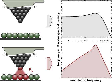
- within this work are written using power spectral densities DX for the quantity X, while simulated and experimental results are described in terms of amplitude spectral densities . Experimental All experiments are performed using a commercial NC-AFM system (UHV 750 variable temperature STM/AFM, RHK


![[Graphic 32]](/bjnano/content/inline/2190-4286-7-181-i73.png?max-width=637&scale=1.18182) wit...
wit...

![[Graphic 34]](/bjnano/content/inline/2190-4286-7-181-i75.png?max-width=637&scale=1.18182) wit...
wit...


Thickness-modulated tungsten–carbon superconducting nanostructures grown by focused ion beam induced deposition for vortex pinning up to high magnetic fields
Beilstein J. Nanotechnol. 2016, 7, 1698–1708, doi:10.3762/bjnano.7.162

- (STM) [20][21]. Recently, De Teresa and Córdoba proposed a strategy to grow W–C films by FIBID with controlled thickness modulation [22], which opens the route for the design of specific experiments probing the behavior of the vortex lattice as a function of magnetic field, temperature and electrical
- O (7%). The nature of the deposits is amorphous, as previous STM and transmission electron microscopy studies have demonstrated [11][13]. The W–C samples have been grown on Si3N4 substrates prepatterned with Ti pads by e-beam evaporation and lift-off techniques for magnetoresistance measurements
- higher temperature. Other weaker local minima are observed at lower fields in specific temperature ranges. Previous STM studies on the W–C superconducting films have given evidence for the vortex-lattice arrangement preferably following an Abrikosov triangular lattice [13][15][20][21][50]. Figure 4b


Hydrophilic silver nanoparticles with tunable optical properties: application for the detection of heavy metals in water
Beilstein J. Nanotechnol. 2016, 7, 1654–1661, doi:10.3762/bjnano.7.157

- ), zeta potential (ζ-potential) measurements and scanning tunneling microscopy (STM). Further, to demonstrate the environmental application of our AgNPs, we also applied them for heavy metal sensing by detecting visible color modification due to SPR spectral changes. We found that these negatively charged
- agent (not reported) was about 60 nm. The broadening of about 30 nm can be ascribed to the surface functionalization of the AgNPs with 3MPS. We characterized the AgNP-3MPS nanoparticles via STM spectroscopy. Figure 3a,b shows the morphology and the profile of the nanoparticles, respectively. We
- <2RH> = 5 ± 2 nm, in good agreement with the STM analysis. The SPR absorption was monitored as a function of the time in order to check the long term stability of the NPs. As shown in Figure 5, the solution presents the same optical spectra 15 days after the preparation, indicating that no aggregation


Scanning probe microscopy studies on the adsorption of selected molecular dyes on titania
Beilstein J. Nanotechnol. 2016, 7, 1642–1653, doi:10.3762/bjnano.7.156

- dianhydride (PTCDA); phtalocyanines; porphyrins; rutile; scanning probe microscopy; scanning tunneling microscopy (STM); titanium dioxide (TiO2); Introduction Today it comes as no surprise that photovoltaic devices can be made of materials other than silicon. Nanocrystalline materials accompanied by organic
- layer [52]. Of the above-mentioned porphyrin species, only 2H-TPP has been studied with STM by Lovat et al. [52]. Similar results were reported by Wang et al. [53]. The molecules adsorb with their plane parallel to the substrate when deposited at room temperature, as expected from the results of the
- NEXAFS measurements. The STM image of a single molecule exhibits two-fold symmetry [52][53]. Molecules are sitting atop the oxygen rows with a common azimuthal orientation in a saddle-shape conformation, which has been identified as the N–N axis parallel to the [001] direction. The most favoured


Advanced atomic force microscopy techniques III
Beilstein J. Nanotechnol. 2016, 7, 1052–1054, doi:10.3762/bjnano.7.98

- microscopy (AFM) celebrates its 30th anniversary this year. It was presented by Binnig, Quate and Gerber in 1986 as an extension of the scanning tunneling microscope (STM) with the possibility to measure forces as small as 10−18 N [1]. Since then many different variations of the force detection method and
- . Combined AFM and STM measurements reveal related force and electronic properties [9], energy dissipation in manipulation processes can be examined via the excitation voltage needed to keep a constant amplitude of the probe oscillation [10][11], pulling forces of atomic or molecular wires can be determined
- surfaces [33], and combined STM and AFM measurements on single-layer graphene on SiC(0001) [34] have been investigated, discussed, and presented. Another combined STM-AFM study determines very accurately the probe-nanocrystal interaction potential [35]. Finally, enhanced information can also be achieved by
Noncontact atomic force microscopy III
Beilstein J. Nanotechnol. 2016, 7, 946–947, doi:10.3762/bjnano.7.86
- tunneling microscopy (STM) relies on quantum mechanical tunneling of electrons to enable the atomic-resolution imaging of (semi-)conducting sample surfaces, it was the atomic force microscope (AFM) that eventually allowed for nanometer-scale imaging of sample surfaces with no limitations on electrical