Search results
Search for "density" in Full Text gives 1512 result(s) in Beilstein Journal of Nanotechnology. Showing first 200.
In situ magnesiothermic reduction synthesis of a Ge@C composite for high-performance lithium-ion batterie anodes
Beilstein J. Nanotechnol. 2023, 14, 751–761, doi:10.3762/bjnano.14.62

- systems have become the most popular energy storage systems, with applications from mobile devices to EVs and grid-scale storage [8][9]. However, the low specific theoretical capacity of graphite limits the energy density of the commercial LIBs [10][11][12][13]. Germanium, as a lithium alloying material


Cross-sectional Kelvin probe force microscopy on III–V epitaxial multilayer stacks: challenges and perspectives
Beilstein J. Nanotechnol. 2023, 14, 725–737, doi:10.3762/bjnano.14.59

- of the surface cross section was achieved thanks to the wide light spot. Finally, the power density was 750 W·m−2 as measured by a thermal power sensor S401C from Thorlabs, which has a flat spectral response in the white-light range of wavelengths. This relatively low power density allows one to
- , and the ϕtip value is set at 5.7 eV, that is, the value measured on our tip as reported above. Note that KELSCAN allows one to simulate VCPD measurements either under dark conditions or under illumination. In the case of “under illumination” simulations, the power density described in the above
- of defects extending into the volume is physically more appropriate than a simpler two-dimensional surface distribution [23]. The introduced defect volume density of states (DOS), N(E) (eV−1·cm−3), is assumed to be homogeneous throughout the thickness of the defective layer, tDL, which we took equal


Metal-organic framework-based nanomaterials as opto-electrochemical sensors for the detection of antibiotics and hormones: A review
Beilstein J. Nanotechnol. 2023, 14, 631–673, doi:10.3762/bjnano.14.52

- already described, the following is a brief outline of some of the desirable qualities of MOFs that are required for developing opto-electrochemical sensors. Electronic properties: Electrostatic potential, density of states, electron density, bandgap, and conductivity are some of a MOF’s crucial
- simulations based on density functional theory with periodic boundary conditions. In comparison to the building units, they noticed that MOFs have a charge distribution that remains constant, and their electronic properties show a wide range of bandgap energies categorized as insulators or semiconductors. The
- behaviour even further. Through variation in temperature resistivity, Clough et al. [83] demonstrated band-like metallic conductivity in cobalt-based MOF. The ferroelectric characteristics of MOFs have not yet been extensively investigated experimentally. However, calculations based on density functional


Suspension feeding in Copepoda (Crustacea) – a numerical model of setae acting in concert
Beilstein J. Nanotechnol. 2023, 14, 603–615, doi:10.3762/bjnano.14.50

- parameters can be presented in a static form by density distributions projected on the (y,z) plane and histograms of the distributions along the y axis accumulated during long-time simulation runs. Figure 8 and Figure 9 present the results of such an accumulation for four cases with extremely different kinds
- of behavior. Darker colors in the grayscale maps correspond to a higher food particle density. Thin curves represent instant snapshots of the particles’ location, and the bold curves represent the number of particles averaged over time, respectively. The panels in Figure 8 illustrate the particle
- fixed angle of rotation ϕmin = −0.4π; the angle of rotation for the long setae was varied. The bold line highlights the curve corresponding to the optimal angle. Density distributions obtained from long-time simulation runs in the (y,z) plane shown by grayscale maps, which were normalized to the density


Transferability of interatomic potentials for silicene
Beilstein J. Nanotechnol. 2023, 14, 574–585, doi:10.3762/bjnano.14.48

- single-layer silicon, polymorphs was examined. Structural and mechanical properties of flat, low-buckled, trigonal dumbbell, honeycomb dumbbell, and large honeycomb dumbbell silicene phases, were obtained using density functional theory and molecular statics calculations with Tersoff, MEAM, Stillinger
- [14]. Ab initio calculations The ab initio calculation methodology here is closely analogous to that used in [15]. Hence, its description is also very similar, that is, density functional theory (DFT) [16][17], ABINIT plane-wave approximation code [18][19], local density approximation (LDA) [20][21
- all previously optimized structures were computed using the metric tensor formulation of strain in the density functional perturbation theory (DFPT) [23]. The mechanical stability of the analyzed structures was verified by calculating the so-called Kelvin moduli [24][25]. To calculate the phonons, the

![[Graphic 3]](/bjnano/content/inline/2190-4286-14-48-i7.svg?max-width=637&scale=1.18182)

ZnO-decorated SiC@C hybrids with strong electromagnetic absorption
Beilstein J. Nanotechnol. 2023, 14, 565–573, doi:10.3762/bjnano.14.47

- diversification of working conditions, new electromagnetic (EM) absorbing materials are gradually designed and fabricated to obtain thinner, lighter, wider, and stronger materials than the traditional materials such as carbonyl iron and ferrite [1][2][3][4]. SiC has the advantages of low density, high-temperature
- carbon shells, as well as ZnO particles growing randomly on the outside (Figure 2a,b). It can be observed that an increasing dosage of ZnNO3·6H2O will lead to an increase in the density of ZnO particles on the carbon structure (Supporting Information File 1, Figure S2), which agrees with the XRD results


SERS performance of GaN/Ag substrates fabricated by Ag coating of GaN platforms
Beilstein J. Nanotechnol. 2023, 14, 552–564, doi:10.3762/bjnano.14.46

- following the procedure described elsewhere [31][32]. The surface morphology depends on the time of photoetching and the overall dislocation density [32]. Next, the fabricated nanostructured GaN platforms were coated with a Ag layer using PLD and MS to form GaN/Ag SERS substrates (Figure 1). To compare SERS
- average intensity of the peak at 1078 cm−1 and the standard deviation of intensity allowed us to determine which samples have the highest enhancement factor (EF) of the Raman signal and a high density of hot spots on the surface. The enhancement factor was calculated according to the formula described in
- method have regions characterized by very high and very low Raman signal enhancements. Therefore, these SERS substrates can be characterized by a lower density of hot spots on their surfaces than PLD-made substrates (Figure 7 and Figure 8). The EF calculated for the 1078 cm−1 peak has similar values in


Nanoarchitectonics to entrap living cells in silica-based systems: encapsulations with yolk–shell and sepiolite nanomaterials
Beilstein J. Nanotechnol. 2023, 14, 522–534, doi:10.3762/bjnano.14.43

- biohybrid system. The microorganisms to be encapsulated were cultivated and 30 mL of culture medium at an optical density of 0.8–1.0 were taken during the exponential growth phase and then centrifuged for 10 min at 8000 rpm and 24 °C. The supernatant was discarded and the cells were re-suspended in 1 mL of
- samples and measuring the density of the supernatant after centrifugation of the culture to remove the suspended solids. Density measurements were performed by weighing 1 mL of supernatant on an analytical balance. It also worth noting that the free-cells culture was inoculated with the equivalent amount
- of biomass immobilized within the silica gel. To perform this calculation, the total optical density of yeast culture used during the silica gel synthesis protocol was considered. The weight of the gel fragment used for production was previously recorded. With this data and the optical density of the


Specific absorption rate of randomly oriented magnetic nanoparticles in a static magnetic field
Beilstein J. Nanotechnol. 2023, 14, 485–493, doi:10.3762/bjnano.14.39

- formula [28][29] where ρ is the density of the magnetic material and is the average magnetization of the assembly of nanoparticles. To obtain statistically reliable results, dynamic hysteresis loops are averaged over 30 independent realizations of the randomly oriented assembly containing 60 non
- , perpendicular to the ac magnetic field (see Figure 3c). As Figure 3d shows, this leads to a sharp drop in the particle hysteresis loop area. In addition to Figure 3, Figure 4 shows the evolution of the surface of the normalized energy density of a nanoparticle, W(θ,φ)/K1V, as a function of the spherical angles
- same for Hdc = 800 Oe. (d) Dynamic hysteresis loops of the nanoparticle for Hdc = 0, 200, 400, and 800 Oe, respectively. Evolution of the normalized energy density of a particle, W(θ,φ)/K1V, as a function of dc magnetic field applied perpendicular to the particle easy anisotropy axis: (a, b) Hdc = 0 Oe


Conjugated photothermal materials and structure design for solar steam generation
Beilstein J. Nanotechnol. 2023, 14, 454–466, doi:10.3762/bjnano.14.36

- can be predicted by density functional theory (DFT) calculations of the conjugated structures. This is an advantage over other carbon materials, even if they are of the same chemical composition [18][19][20][21][22]. We review the recent progress in the material development of conjugated solar
- constructing electron donor–acceptor pairs. Density functional theory (DFT) simulations indicated donor–acceptor interactions between arginine and PDA subunits, including the formation of 5,6-dihydroxyindole (DHI) and indole-5,6-quinone (IQ). Dopamine and arginine were copolymerized in an aqueous solution at


Molecular nanoarchitectonics: unification of nanotechnology and molecular/materials science
Beilstein J. Nanotechnol. 2023, 14, 434–453, doi:10.3762/bjnano.14.35

- epitaxial polymerization, controlling the length, density, bonding, and propagation direction of the molecules. Advances in surface scanning probe microscopy techniques have enabled the synthesis and analysis of unstable short-lived products by local probe synthesis as well as direct observation of
- . Foster, Kawai, and co-workers have investigated the zero-bias peak at the center of an armchair-type graphene nanoribbon on a AuSix/Au(111) surface using a combination of low-temperature scanning tunneling microscopy/spectroscopy and density functional theory calculations [116]. The zero-bias peak at the


Evaluation of electrosynthesized reduced graphene oxide–Ni/Fe/Co-based (oxy)hydroxide catalysts towards the oxygen evolution reaction
Beilstein J. Nanotechnol. 2023, 14, 420–433, doi:10.3762/bjnano.14.34
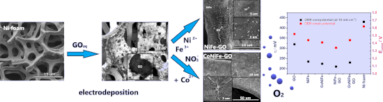
- ]. Afterwards, the current density tended to stabilize for NiFe and CoNiFe, which may be associated with the steady-state formation of the catalyst film on the metallic surface. The addition of cobalt to NiFe resulted in a lower overall current density during the synthesis process. In the case of the deposition
- of NiFe and CoNiFe on GO/nickel foam, the specific current density peak appeared after around 8 s and 20 s of the deposition for CoNiFe-GO and NiFe-GO, respectively. Because the metallic films were deposited on the surface of nickel foam already modified with GO, the peak may be associated with the
- reduction process of the already deposited GO. Afterwards, the current density increased due to the film formation, and then it gradually stabilized over time. A different chronoamperometric trend can be observed in the case of the electrodeposition of GO on the surface of nickel foam (Figure 1a inset). In


Plasmonic nanotechnology for photothermal applications – an evaluation
Beilstein J. Nanotechnol. 2023, 14, 380–419, doi:10.3762/bjnano.14.33

- materials [7][8], such as Au nanoparticles (AuNPs), in photodynamic therapy [9][10][11]. Metal nanoparticles in general have been extensively explored in PPT applications due to their high free electron density and the possibility of intricate tuning of light absorption [12]. Noble metal nanoparticles with
- curvature [35]. Finally, changes to the material composition, such as through doping or vacancy processing, can affect the LSPR because of changes in the free electron density, the electron effective mass, and the electronic band structure in general [36][37]. An understanding of the changes in absorbance
- is the polarization density. P can be arrived at by solving the equation of motion for a single electron as Hence the expression relating the dielectric displacement (D) and the external electric field can be obtained as where is the natural frequency of oscillation of the electron cloud. Comparing


Quercetin- and caffeic acid-functionalized chitosan-capped colloidal silver nanoparticles: one-pot synthesis, characterization, and anticancer and antibacterial activities
Beilstein J. Nanotechnol. 2023, 14, 362–376, doi:10.3762/bjnano.14.31

- acid hydrate, Cell Proliferation Kit II test (Roche). XTT solution was added to each plate at 50 µL and was incubated for 4 h at 37 °C. Then, the absorbance (optical density, OD) of the solution in each plate was read at 450 nm by a spectrophotometer (BiotekELx800, Winooski, VT, USA). Statistical


Polymer nanoparticles from low-energy nanoemulsions for biomedical applications
Beilstein J. Nanotechnol. 2023, 14, 339–350, doi:10.3762/bjnano.14.29

- roughly estimated by [18]: where Ms is the surfactant molecular weight, as is the area occupied per surfactant molecule at the O/W interface, NA is Avogadro’s number, ρ0 is the density of the oil phase, Ros is the oil/surfactant mass ratio, and vL is the molar volume of the hydrophobic part of the
- solubility of polymers in the used solvents rarely exceeds 10 wt %). Experimental dP/dE ratios are above of those expected if the nanoparticles were to be obtained with a density equal to that of the polymer in the bulk, that is, by applying the formula where mP/mT is the polymer/solvent mass ratio and ρT/ρP
- is the solvent/polymer bulk density ratio (this equation assumes that each droplet generates one single nanoparticle). In other words, the polymer nanoparticles seem to be, in general, less dense than in the bulk, which could be attributed to porosity generated during solvent evaporation


Overview of mechanism and consequences of endothelial leakiness caused by metal and polymeric nanoparticles
Beilstein J. Nanotechnol. 2023, 14, 329–338, doi:10.3762/bjnano.14.28

- effectiveness of NanoEL closely depends on the physicochemical properties of the NPs such as size, shape, density, and surface charge [12][19][20][21]. Moreover, it is worth to mention that the biological effects of NPs to endothelial cells also depend on the microenvironments. The adhesion of proteins and/or
- induction depends on the density of NPs, where the effective density of Si NPs ranged from 1.57 to 1.72 g/cm3 [20]. The leakage rate increases with increasing nanoparticle density. They also showed that a force of approximately 1.8 nN/μm along the boundaries of VE-cad adherens junctions mediated by


Bismuth-based nanostructured photocatalysts for the remediation of antibiotics and organic dyes
Beilstein J. Nanotechnol. 2023, 14, 291–321, doi:10.3762/bjnano.14.26

- surface charge, low carrier density, small electron effective mass, long electron mean free path, and extremely low band overlap energy, bismuth can transition from a semimetal to a semiconductor by shrinking its crystallite size [25][71][72][73][74][75][76][77]. To hasten the separation of photogenerated
- important for electronic transport and semimetal-to-semiconductor transition, as well as its highly anisotropic Fermi surface (with an electron and hole Fermi energies of 27.2 and 10.8 meV, respectively), which results in an extremely low carrier density of around 3 × 1017 cm−3 [78] and very little overlap
- semiconductor and a noble metal with an appropriate work function. A unidirectional charge transfer is enabled by the Schottky potential barrier, increasing charge density and separation [72]. Shen et al. [166] created a Schottky junction by synthesising NiSe2 nanosheets on top of BiVO4 nanosheets using a


Biocatalytic synthesis and ordered self-assembly of silica nanoparticles via a silica-binding peptide
Beilstein J. Nanotechnol. 2023, 14, 280–290, doi:10.3762/bjnano.14.25

- combination with NH3. The reaction kinetics were monitored via measuring the optical density (OD) with UV–vis spectroscopy and the conversion of substrate via gas chromatography coupled with mass spectroscopy (GC–MS). Size and net surface charge distribution of the particles were determined with dynamic light
- with different concentrations of the peptide to examine whether the peptide had a synergistic effect on the formation of SiO2 particles. Kinetic measurements The reaction rates were monitored by measuring the optical density (OD) of the particles at 445 nm (Varioskan Flash micro-plate reader, Thermo


Spin dynamics in superconductor/ferromagnetic insulator hybrid structures with precessing magnetization
Beilstein J. Nanotechnol. 2023, 14, 233–239, doi:10.3762/bjnano.14.22

- a standard procedure [29]: where is the spin operator in electron–hole–spin space, g is the gyromagnetic ratio for free electrons, μB is the Bohr magneton, N0 is the density of states at the Fermi level, and is the Fourier–Winger transform of the Green’s function [29][30] The expression for the
- . However, there is a possibility to induce stationary pure spin currents inside trilayer superconducting structures [1]. The distributions of spin current amplitudes into the S layer are depicted in Figure 2. The amplitudes are normalized by the factor js0 = (ℏ/2e)je0. The charge current density
- spin relaxation processes, but we do not take into account any spin relaxation mechanisms within our model for a superconductor. We should mention that both spin pumping mechanisms in superconductors and normal metals are determined by the penetration of nonequillibrium spin density from the interface


Cyclodextrins as eminent constituents in nanoarchitectonics for drug delivery systems
Beilstein J. Nanotechnol. 2023, 14, 218–232, doi:10.3762/bjnano.14.21

- charges of high density can damage the membranes and organelles of normal cells. With the use of CyD-based DDSs, however, high transfection efficiency and low cytotoxicity have been accomplished with minimal immune stimulation. The preorganized three-dimensional molecular structure of CyD as well as the


A novel approach to pulsed laser deposition of platinum catalyst on carbon particles for use in polymer electrolyte membrane fuel cells
Beilstein J. Nanotechnol. 2023, 14, 190–204, doi:10.3762/bjnano.14.19

- graphitization were used as carbon supports. The best electrochemical measurement results were obtained for Pt deposited on Vulcan XC-72R. The peak power density measured for this material in a membrane electrode assembly (MEA) of a PEMFC (fed with H2/Air) was 0.41 W/cm2, which is a good result compared to 0.57
- and an electrochemical catalyst for electrochemical reactions under low temperatures, are typically used in automobiles and portable electronics [4][5]. The primary application potential is related to their compact size, lightweight, high power density, and low operating temperature. However, they
- and physical methods of Pt deposition [22][23][24][25][26]. Direct deposition of Pt onto carbon supports resulting in a thin catalyst layer and good dispersion of formed Pt nanoparticles (PtNPs) is of particular interest because it should allow for a high Pt mass-specific power density to be achieved


High–low Kelvin probe force spectroscopy for measuring the interface state density
Beilstein J. Nanotechnol. 2023, 14, 175–189, doi:10.3762/bjnano.14.18

- of the effects of semiconductor interface states with high spatial resolution using high and low AC bias frequencies compared with the cutoff frequency of the carrier transfer between the interface and bulk states. Information on the energy spectrum of the interface state density is important for
- interface state density inside semiconductors. We derive an analytical expression for the electrostatic forces between a tip and a semiconductor sample in the accumulation, depletion, and inversion regions, taking into account the charge transfer between the bulk and interface states in semiconductors. We
- show that the analysis of electrostatic forces in the depletion region at high- and low-frequency AC bias voltages provides information about the interface state density in the semiconductor bandgap. As a preliminary experiment, high-low KPFS measurements were performed on ion-implanted silicon


A distributed active patch antenna model of a Josephson oscillator
Beilstein J. Nanotechnol. 2023, 14, 151–164, doi:10.3762/bjnano.14.16

- spatial distribution of the input current density in a JJ, described by the perturbed sine-Gordon equation. In the presence of a magnetic field and fluxons, the oscillating current is distributed nonuniformly within the junction. This nonuniformity is essential for the FFO operation. It determines the
- density through the JJ, which has Cooper pair and quasiparticle (QP) components, Here, Jc0 is the Josephson critical current density, η is the Josephson phase difference, and rQP = RQPab is the QP resistance per unit area. Active patch antenna model of a junction Equation 1 is the equation for an active
- TL [37] with a distributed feed-in current density Jz. Therefore, a JJ has many similarities with the microstrip patch antenna. However, there are three main differences: (i) The feed-in geometry. A patch antenna has a point-like feed-in port, through which the oscillating current is applied [34][35


Batch preparation of nanofibers containing nanoparticles by an electrospinning device with multiple air inlets
Beilstein J. Nanotechnol. 2023, 14, 141–150, doi:10.3762/bjnano.14.15

- shrink and bend as much as possible, and the change of external electric field would interact with the accumulated charges on the polymer fluid surface, making the charge density on the charged fluid surface uneven. Accordingly, the formulas to calculate these three forces are as follows: where ρ is the
- density of spinning solution (kg/m3), g is the gravitational acceleration (m/s2), h is the fluctuation height of the polymer spinning solution (m), γ is the surface tension coefficient of the spinning solution (N/m), ε0 is vacuum dielectric constant, E0 is the edge electric field intensity (V/m), Ep is


Characterisation of a micrometer-scale active plasmonic element by means of complementary computational and experimental methods
Beilstein J. Nanotechnol. 2023, 14, 110–122, doi:10.3762/bjnano.14.12

- polaritons (SPPs) are mixed states of photons and electron density waves propagating along the interface between a conductor and a dielectric. As a result of this phenomenon, an electric field strongly confined in the z-direction is produced at the interface. As direct excitation of a smooth metallic surface
- contraction per point for the lock-in amplifier to integrate over. The time constant for the lock-in process was set to 10 ms to match the time the tip is over each pixel. The sensitivity of the LIA was set to 200 μV. The applied voltage was set based on the current density through the sample so as to match
- surrounding the sample as a function of applied current. For higher current densities, a wider distribution of the temperature is expected. A current buffer was used to ensure the current density through the element was consistent throughout an AFM scan. The probe was left electrically floating during


