Search results
Search for "electron" in Full Text gives 1789 result(s) in Beilstein Journal of Nanotechnology. Showing first 200.
ZnO-decorated SiC@C hybrids with strong electromagnetic absorption
Beilstein J. Nanotechnol. 2023, 14, 565–573, doi:10.3762/bjnano.14.47

- filler load of 20 wt % for all SCZ samples. This indicates that multiple dielectric relaxation processes (such as Maxwell–Wagner relaxation and electron polarization) may occur when the electromagnetic waves interact with the materials [31]. The plots of ε′ and ε″ for all samples are quasi-linear


SERS performance of GaN/Ag substrates fabricated by Ag coating of GaN platforms
Beilstein J. Nanotechnol. 2023, 14, 552–564, doi:10.3762/bjnano.14.46

- substrates were examined regarding their optical properties using UV–vis spectroscopy and regarding their morphology using scanning electron microscopy. SERS properties of the fabricated GaN/Ag substrates were evaluated by measuring SERS spectra of 4-mercaptobenzoic acid molecules adsorbed on them. For all
- morphology of fabricated Ag layers examined by scanning electron microscopy (SEM). Then, we present the results of their optical properties determined using UV–vis spectroscopy. Finally, we compare the SERS performance of the GaN/Ag substrates toward 4-mercaptobenzoic acid (pMBA) molecules adsorbed on them
- GaN/Ag substrates The morphology of the fabricated GaN/Ag substrates was visualized using a scanning electron microscope (SEM) (Quanta 3D FEG, FEI Company, Eindhoven, Netherlands). The thickness of the reference Ag layers, deposited on flat silicon substrates at room temperature, was measured with an


Observation of multiple bulk bound states in the continuum modes in a photonic crystal cavity
Beilstein J. Nanotechnol. 2023, 14, 544–551, doi:10.3762/bjnano.14.45

- To verify the multiple modes in the bandgap mirror-assisted BIC cavity, several samples with different sidelengths (w) were fabricated by electron beam lithography (EBL) and inductively coupled plasma (ICP) etching on 500 nm thick AlGaAs on a sapphire wafer. The parameter sweep of w around 400 nm was
- carried out to compensate for deviations between fabricated and designed values. To obtain devices with larger Q factors and higher scattering power, cavities with larger Na = 30 and Nb = 10 were fabricated. Optical and scanning electron microscopy (SEM) images are given in Figure 3a. A microscope was
- all bulk modes. (d) The near-field H field intensity distribution of modes M11 to M44. The yellow dashed squares indicate the boundary of region A. Fabricated samples and optical setup. (a) Optical and scanning electron microscopy images of fabricated samples, scale bar: 10 μm. (b) Diagram of the


Carbon nanotube-cellulose ink for rapid solvent identification
Beilstein J. Nanotechnol. 2023, 14, 535–543, doi:10.3762/bjnano.14.44

- length of 5 μm were produced at CTNano/UFMG [59][60][61]. Morphological analysis was carried out by scanning electron microscopy (SEM) in a Quanta 200 FEG, using secondary electrons between 2 and 10 kV. Atomic force microscopy (AFM) was carried out on a Bruker MultiMode8 SPM using the intermittent
- pressure of the solvents controls the time the liquid will stay within the sensor before it evaporates. This makes it a key factor regarding the swelling process of the CPC matrix and the electron tunneling process. To investigate this hypothesis, we designed an experiment to mimic the thermal effects


Nanoarchitectonics to entrap living cells in silica-based systems: encapsulations with yolk–shell and sepiolite nanomaterials
Beilstein J. Nanotechnol. 2023, 14, 522–534, doi:10.3762/bjnano.14.43

- systems were studied by means of optical and electron microscopy (SEM and FE-SEM). Both techniques allowed us to study in detail the cellular arrangement of the microorganisms and their interaction with the inorganic matrix system. FE-SEM microscopy images of the different gel encapsulation systems are
- without staining. Electron microscopy imaging was conducted using a field-emission scanning electron microscope FEI-NOVA NanoSEM 230 equipped with an Apollo XL silicon drift detector from EDAX-Ametek or using a high-resolution JEOL IT500HR/LA microscope equipped with an energy dispersive X-ray


On the use of Raman spectroscopy to characterize mass-produced graphene nanoplatelets
Beilstein J. Nanotechnol. 2023, 14, 509–521, doi:10.3762/bjnano.14.42

- widely used characterization tool for GR2Ms [8]. A search of Web of Science showed that of 97,532 articles published in the last five years with “Graphene” in the abstract, 9.3% also mentioned “Raman”. This is compared with atomic force microscopy (AFM) (2.4%), scanning electron microscopy (SEM) (11.4
- %), transmission electron microscopy (TEM) (7.2%) or X-ray photoelectron spectroscopy (XPS) (5.6%). It has the advantages of relatively low cost, simple sample preparation, quick measurements, and automated analysis, offering clear benefits for quality control applications. It has been demonstrated in several


The origin of black and white coloration of the Asian tiger mosquito Aedes albopictus (Diptera: Culicidae)
Beilstein J. Nanotechnol. 2023, 14, 496–508, doi:10.3762/bjnano.14.41

- analysed using scanning electron microscopy, transmission electron microscopy, and fluorescence microscopy. Reflectance spectra of the white areas are measured. No clear difference is present in the morphology of micro- and nanostructures of black and white scales in SEM and TEM, but black scales contain a
- . The ultrastructure of the white and black scales on the hindlegs of Ae. albopictus is analysed using scanning electron microscopy, transmission electron microscopy, and fluorescence microscopy. Moreover, reflectance spectra of the white areas are measured. The scales are present also on other body
- (Figure 4b–d,h). Such nanovoids originate from the rests of epidermal cells and appear in TEM as white or light grey areas inside the scales, together with electron-dense debris (Figure 4h). Their occurrence is higher at the bases of microribs, because the cuticle thickness is higher there (Figure 4h


A mid-infrared focusing grating coupler with a single circular arc element based on germanium on silicon
Beilstein J. Nanotechnol. 2023, 14, 478–484, doi:10.3762/bjnano.14.38

- than that of a MIR grating coupler with conventional tapered linear gratings (5.49%). Because the proposed structure is geometrically simple, it is easy to implement experimentally. The proposed MIR FGC based on Ge-on-Si can be fabricated by electron beam lithography (EBL) and inductively coupled


Mixed oxides with corundum-type structure obtained from recycling can seals as paint pigments: color stability
Beilstein J. Nanotechnol. 2023, 14, 467–477, doi:10.3762/bjnano.14.37

- results. The Raman modes are A1g (ca. 149 cm−1 and ca. 501 cm−1) and E1g (ca. 222 cm−1, ca. 290 cm−1, ca. 298 cm−1, ca. 402 cm−1, and ca. 615 cm−1, where 290 cm−1 and 298 cm−1 usually are a doublet with E1g symmetry and cannot be easily resolved [20]. Scanning electron microscopy (SEM) The morphology of
- -performance detector, with a power of 300 W. A scanning electron microscope Hitachi SU8020 SEM (Tokyo, Japan) was used to obtain morphology information. The oxidation state and composition of the chemical elements at the surface were evaluated by X-ray photoelectron spectroscopy (XPS) (Versaprobe PHI 5000
- the four vibrational modes E1g characteristic of Cr2O3, and (b) sample 2, which features the seven characteristic vibrational modes (two A1g modes and five E1g modes) of Fe2O3. Scanning electron microscopy images of (a) sample 1 (low magnification, SE detector), (b) sample 1 (high magnification, SE


Conjugated photothermal materials and structure design for solar steam generation
Beilstein J. Nanotechnol. 2023, 14, 454–466, doi:10.3762/bjnano.14.36

- semiconductor materials, optical absorption significantly varies with the wavelength, depending on the bandgap energy. When semiconductor materials are irradiated with light, electron–hole pairs with energies close to the bandgap are produced. The excited electrons eventually return to a lower energy state and
- dyes, such as cyanines, croconaines, and diketopyrrolopyrroles (DPPs), have been evaluated for PTMs because of their intense absorption in the NIR range. These materials consist of long conjugated groups that are bridging electron donors or acceptors. The absorption properties of these PTMs can be
- photophysical properties and hydrophobicity through organic reactions. In general, DPP dyes have high photoluminescence quantum yields, but they have a relatively low photostability, degrading after 150 min under a collimated 300 W Xe lamp light source. It was previously reported that introducing electron


Molecular nanoarchitectonics: unification of nanotechnology and molecular/materials science
Beilstein J. Nanotechnol. 2023, 14, 434–453, doi:10.3762/bjnano.14.35

- greatly to the elucidation of the elementary processes of materials synthesis. The development of observation and analysis techniques for ultrasmall structures by nanotechnology has clarified processes of materials creation. For example, as summarized in a recent review by Harano, electron microscopic


Evaluation of electrosynthesized reduced graphene oxide–Ni/Fe/Co-based (oxy)hydroxide catalysts towards the oxygen evolution reaction
Beilstein J. Nanotechnol. 2023, 14, 420–433, doi:10.3762/bjnano.14.34
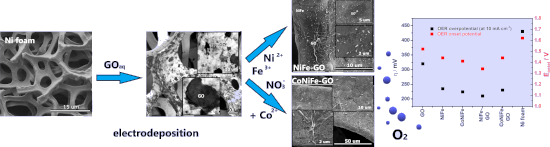
- graphene material with Ni-, Fe- and/or Co-based oxides/hydroxides with high chemical reactivity provides both an effective electron pathway through the catalyst [20] and high specific surface area [21], which is desirable for the OER process [13]. The overall electrocatalytic performance of the hybrid
- OER catalyst of Gr/NiFe layered double hydroxide (LDH) was chemically fabricated on a GCE. The catalyst revealed an OER Eonset of 1.48 V vs RHE and η of 250 mV determined in 0.1 M KOH. Improved electron transport was provided by the graphene material in the catalyst structure. Enhanced OER catalytic
- NiFe-LDH/RGO/NF, respectively. The efficient OER was associated with the presence of the electron interaction between the metal and graphene. The literature presents the possibility of improving OER performance of the electrode by combining Fe-, Ni- and/or Co-based oxides/hydroxides and GO instead of


Plasmonic nanotechnology for photothermal applications – an evaluation
Beilstein J. Nanotechnol. 2023, 14, 380–419, doi:10.3762/bjnano.14.33

- materials [7][8], such as Au nanoparticles (AuNPs), in photodynamic therapy [9][10][11]. Metal nanoparticles in general have been extensively explored in PPT applications due to their high free electron density and the possibility of intricate tuning of light absorption [12]. Noble metal nanoparticles with
- not absorbed by generic PT materials can be utilized for absorption and eventual conversion into heat by incorporation of plasmonic nanoparticles of appropriate sizes and shapes. Plasmons, that is, collective electron excitations, are either excited in the bulk of the material (volume plasmons) or on
- effective localization of the incident photon energy, and the decay of this oscillation (through phenomena such as electron–electron, electron–phonon, and electron–surface scattering) releases the absorbed energy into the lattice as heat (or as photons), often making them efficient tunable PT energy


Quercetin- and caffeic acid-functionalized chitosan-capped colloidal silver nanoparticles: one-pot synthesis, characterization, and anticancer and antibacterial activities
Beilstein J. Nanotechnol. 2023, 14, 362–376, doi:10.3762/bjnano.14.31

- infrared (FTIR) spectroscopy, and transmission electron microscopy (TEM). The characteristic surface plasmon resonance (SPR) absorption band has been found at 417 and 424 nm for Ch/Q- and Ch/CA-Ag NPs, respectively. The formation of a chitosan shell comprising quercetin and caffeic acid, which surround the
- of quercetin, caffeic acid, chitosan, Ch/Q-, and Ch/CA-Ag NPs were monitored using a Perkin Elmer Spectrum Two FTIR-ATR spectrophotometer in the range of 4000–400 cm−1. Transmission electron microscopy (TEM) measurements were performed with a JEOL JEM-2100 electron microscope operating at 200 kV
- TEM due to energetic electron bombardment causing burn, negative staining using uranyl acetate was performed. Figure 4d shows the TEM image of the Ch/Q-Ag NPs exposed by negative staining. It is seen that the chitosan/quercetin shell structure uniformly covers the core Ag NPs (see insets of Figure 4d


The steep road to nonviral nanomedicines: Frequent challenges and culprits in designing nanoparticles for gene therapy
Beilstein J. Nanotechnol. 2023, 14, 351–361, doi:10.3762/bjnano.14.30

- cells. (f) Annual prevalence of reporting imaging and (or) flow cytometry during the last five years. Of note, “imaging” refers to images captured by widefield fluorescence microscopy or confocal microscopy (electron microscopy excluded). See details about experimental approach and scope in Supporting


Bismuth-based nanostructured photocatalysts for the remediation of antibiotics and organic dyes
Beilstein J. Nanotechnol. 2023, 14, 291–321, doi:10.3762/bjnano.14.26

- a nutshell, when exposed to light of the desired wavelength (enough energy), an electron (e−) in the photocatalyst's valence band absorbs photon energy and is excited to the conduction band on a femtosecond scale. This results in the formation of a hole (h+) in the valence band and a charge carrier
- pair (e− and h+) on the surface of the photocatalyst. Three possibilities exist at this point: (a) The generated charge carriers recombine and generate heat, (b) the generated interfacial charge carriers simultaneously reduce and oxidise contaminants, or (c) the generated charge carrier and an electron
- donor or acceptor on the surface of the photocatalyst may continue to interact. Nothing happens in the first scenario. In the second scenario, an electron or hole interacts with dissolved oxygen or water to produce ROS (e.g., •OH, O2•−). These ROS play a significant role in the photo-oxidation/reduction


Biocatalytic synthesis and ordered self-assembly of silica nanoparticles via a silica-binding peptide
Beilstein J. Nanotechnol. 2023, 14, 280–290, doi:10.3762/bjnano.14.25

- scattering (DLS). The efficiency of the self-assembly was evaluated with scanning electron microscopy (SEM), UV–vis spectroscopy, and qualitative visual demonstration. Results and Discussion SiBP alone as catalyst Reaction kinetics were studied via OD measurements of the particles and GC analysis of
- covers were moved completely out of the colloidal solution. Scanning electron microscopy To analyze as-synthesized particles, 50 µL aliquots of the reaction solutions were placed on standard microscope cover slides. The excess liquid was removed by absorbing on a clean absorbent paper. To analyze self


Spin dynamics in superconductor/ferromagnetic insulator hybrid structures with precessing magnetization
Beilstein J. Nanotechnol. 2023, 14, 233–239, doi:10.3762/bjnano.14.22

- a standard procedure [29]: where is the spin operator in electron–hole–spin space, g is the gyromagnetic ratio for free electrons, μB is the Bohr magneton, N0 is the density of states at the Fermi level, and is the Fourier–Winger transform of the Green’s function [29][30] The expression for the
- the free electron gas value N0 ≈ 4.9·1046 J−1·m−3. The coherence length has been estimated using , where kB is the Boltzmann constant and ξ0 ≈ 11 nm. We numerically solve Equation 1 in mixed representation with the normalization condition. To obtain physical observables from the quasiclassical Green’s
- induced magnetization dynamics on the electron perturbations in the S film. The dynamics of any observable will be periodic and can be characterized by its amplitude value. Thus, we only need to calculate the doubled absolute value of the coefficients in Equation 6 and Equation 7, which are exactly the


A novel approach to pulsed laser deposition of platinum catalyst on carbon particles for use in polymer electrolyte membrane fuel cells
Beilstein J. Nanotechnol. 2023, 14, 190–204, doi:10.3762/bjnano.14.19

- recorded using a rotating electrode with an RRDE ring [42]. The number of electron was calculated as: while the amount of hydrogen peroxide was calculated from the equation: where ID is the disc current, IR is the ring current, and η is the electrode collection coefficient. The results of RRDE measurements
- . Materials A, C, and D are characterized by a higher percentage of the two-electron reduction of oxygen in the mechanism than in the case of the commercial catalyst, which translates into a higher contribution of hydrogen peroxide in the reaction products (Figure 5d). Material C excels in this comparison
- , which is consistent with its composition, namely the lowest amount of platinum on the surface, which is responsible for the four-electron reduction of oxygen, and a significant fraction in the reaction of active carbon centers, which reduce oxygen in a two-electron process. The best performance was


High–low Kelvin probe force spectroscopy for measuring the interface state density
Beilstein J. Nanotechnol. 2023, 14, 175–189, doi:10.3762/bjnano.14.18

- given by Similar results can be obtained for a p-type semiconductor. Next, we consider the charge Qit due to the interface states. In indirect-bandgap semiconductors such as Si with a low carrier density below 1017 cm−3, the charge (electron and hole) transfer between the interface and bulk states at
- low carrier density can be explained by the model with Shockley–Read–Hall (SRH) statistics [25][26]. This model is based on the charge capture and emission between the interface and bulk states (Figure 2). Assume that and are the capture rates for electrons and holes per electron and hole
- , respectively, when all interface states are unoccupied, and and are the emission rates for electrons and holes per electron and hole, respectively. The capture rates per unit volume for electrons and holes ( and ) are given by [25][26] where fit is the fraction of occupied interface states. n and p are the


Structural, optical, and bioimaging characterization of carbon quantum dots solvothermally synthesized from o-phenylenediamine
Beilstein J. Nanotechnol. 2023, 14, 165–174, doi:10.3762/bjnano.14.17

- surface states, precursors, preparation methods, and heteroatom doping [9]. Previous investigations showed that possible mechanisms of the CQD photoluminescence are radiative recombination of electron–hole pairs in the sp2 domains inside the sp3 matrix as well as the effect of zig-zag edges [6][18]. Apart
- through energy transfer to molecular oxygen [21]. Chong et al. claimed that superoxide anions are involved in the generation of singlet oxygen, implying that electron transfer is an intermediate step for the generation of singlet oxygen by photoexcited graphene quantum dots [20]. In nitrogen-doped
- −polyoxypropylene−polyoxyethylene Pluronic 68 generate singlet oxygen through energy transfer to molecular oxygen [21]. But CQDs prepared from o-phenylenediamine do not generate singlet oxygen or OH radicals through energy or electron transfer, because the condensation process of these dots includes NH2 groups in


Batch preparation of nanofibers containing nanoparticles by an electrospinning device with multiple air inlets
Beilstein J. Nanotechnol. 2023, 14, 141–150, doi:10.3762/bjnano.14.15

- using an electronic balance (XJ120A, Precisa LTD.). The nanofiber morphology was investigated by a scanning electron microscopy (SEM, Hitachi S4800, Hitachi LTD.), and Image J software (National Institute of Mental Health) was used to characterize the fiber diameter distribution by random selection of


Formation of nanoflowers: Au and Ni silicide cores surrounded by SiOx branches
Beilstein J. Nanotechnol. 2023, 14, 133–140, doi:10.3762/bjnano.14.14

- small pieces were ready for thin film deposition. Metallic bilayers of Au and Ni of three different thickness ratios and a total thickness of 20 nm were deposited onto the SiO2/Si substrate by electron beam evaporation (CS400ES, VON ARDENNE) at a working pressure of 1 × 10⁻⁶ mbar. The Au layer was
- annealed at 1050 °C was named 15Au5Ni. The morphology was imaged by optical microscopy (OM, Zeiss Axiotech) and high-resolution scanning electron microscopy (HR-SEM, Hitachi S-4800) equipped with energy-dispersive X-ray spectroscopy (EDS, Thermo Scientific). The SEM images were recorded by using mixed


Characterisation of a micrometer-scale active plasmonic element by means of complementary computational and experimental methods
Beilstein J. Nanotechnol. 2023, 14, 110–122, doi:10.3762/bjnano.14.12

- polaritons (SPPs) are mixed states of photons and electron density waves propagating along the interface between a conductor and a dielectric. As a result of this phenomenon, an electric field strongly confined in the z-direction is produced at the interface. As direct excitation of a smooth metallic surface


Antimicrobial and mechanical properties of functionalized textile by nanoarchitectured photoinduced Ag@polymer coating
Beilstein J. Nanotechnol. 2023, 14, 95–109, doi:10.3762/bjnano.14.11

- [10]), gold [11][12], zinc oxide [13][14], and especially silver nanoparticles [15][16][17][18]. Silver is known to target peptidoglycane, a cellular membrane component of Gram-negative and -positive bacteria. If introduced directly in its ionic form, silver interacts with the electron-donor groups of
- electron microscopy (SEM), transmission electron microscopy (TEM), and reflectance measurements to assess the optical properties and the durability of the functionalized textiles. Results and Discussion Photoinduced synthesis of the Ag@polymer coating Specific monomers poly(ethylene glycol) 600 diacrylate
- , as well as the final thickness of the metallic layer, account for this difference in reflectivity. Scanning electron microscopy (SEM) carried out on the surface of functionalized textiles revealed the homogenous distribution of AgNPs, with average sizes of 62 ± 2 nm and 58 ± 1 nm for the Ag@PEG600DA


