Search results
Search for "electron microscopy" in Full Text gives 1257 result(s) in Beilstein Journal of Nanotechnology. Showing first 200.
Nanoglasses: a trail towards uncharted regions of vitreous materials and their properties?
Beilstein J. Nanotechnol. 2026, 17, 1047–1062, doi:10.3762/bjnano.17.72
- tens of nanometres. Given a thickness of the glass–glass interfaces of the order of a few nanometres, it is expected that different structural arrangements exist within the grains in comparison to the glass–glass interfaces; this has been confirmed recently by so-called fluctuation electron microscopy
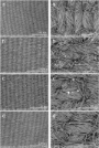
- a transmission electron microscope (TEM), so that projection artefacts that are inherent in the analysis of powder-compacted nanoglasses can be avoided. Figure 3a presents a scanning electron microscopy (SEM) overview of the columnar nanoglass thin films, highlighting their overall structural
- . Further confirmation of these distinct phases is provided by the cross-sectional high-angle annular dark-field scanning transmission electron microscopy (HAADF-STEM) image in Figure 3c, which differentiates the glass grains and the glass–glass interface regions based on contrasting dark and bright areas


Influence of an external electric field on the catalytic CO oxidation of nanoscaled CeO2 and its La3+ and Gd3+ congeners
Beilstein J. Nanotechnol. 2026, 17, 1028–1038, doi:10.3762/bjnano.17.70
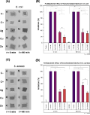
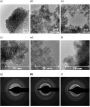
- Information File 1, Figures S20–S24). All cerium oxide nanoparticles are strongly aggregated and form dense strongly corrugated films with an agglomerated particle size of about 50 nm in scanning electron microscopy (SEM) (Supporting Information File 1, Figure S25). Transmission electron microscopy (TEM) and
- high-resolution transmission electron microscopy (HRTEM) reveal highly crystalline spherical, slightly faceted nCeO2 and 5% doped-nCeO2 with a diameter of around 15 nm (Figure 1a–c). The observed d-spacings are characteristic of nCeO2 (0.31 nm), Gd3+–nCeO2 (0.31 nm), and La3+–nCeO2 (0.29 nm) (Figure 1d


Synthesis and characterization of RF-sputtered ZnTe/Cu2−xTe thin films for solar cell applications
Beilstein J. Nanotechnol. 2026, 17, 1016–1027, doi:10.3762/bjnano.17.69
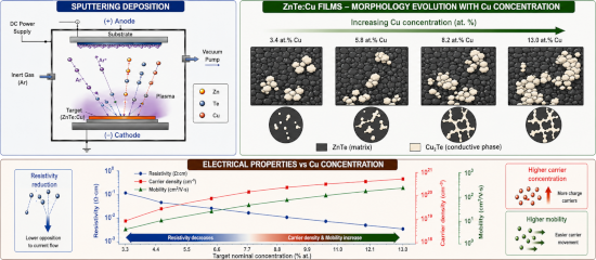
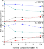
- produced only minor lattice modifications, while higher Cu and O contents promoted the formation of Cu2−xTe secondary phases, as confirmed by Raman spectroscopy, grazing-incidence X-ray diffraction and scanning electron microscopy. Optical measurements showed a significant reduction in infrared
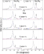
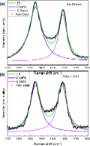
- . Vibrational and structural surface properties Figure 4 shows Raman spectra and a scanning electron microscopy (SEM) image of the CuZnTeO film grown at 300 °C with a nominal Cu and O concentration of 3 atom %. The SEM image reveals an irregular surface morphology characterized by agglomerate formation with non



Ultrasonic irradiation in the synthesis of nanohydroxyapatite: a chemically friendly technique for improving hemocompatibility and antibiofilm applications
Beilstein J. Nanotechnol. 2026, 17, 991–1015, doi:10.3762/bjnano.17.68
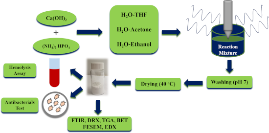
- quantitative analysis of particle size was conducted using field-emission scanning electron microscopy (FESEM) and BET surface area measurements. These findings, along with their corresponding statistical evaluations, are presented and extensively discussed in section “Field emission scanning electron
- only undergoes transformations leading to its decomposition at temperatures above 1000 to 1300 °C; this promotes the formation of other biocompatible phosphate species, such as tetracalcium phosphate and tricalcium phosphate [77]. Field-emission scanning electron microscopy and particle size
- the material’s performance in biological assays, such as hemocompatibility and antibacterial activity. The particle size, as discussed in the preceding paragraphs, can be determined statistically through electron microscopy imaging, as well as by calculating the specific surface area of the




Materials challenges in solid-state sensors for continuous monitoring of ions in water
Beilstein J. Nanotechnol. 2026, 17, 935–973, doi:10.3762/bjnano.17.66



Enhanced erosion resistance and radiation stability of WC–WO3 nanocomposite films under 100 keV Kr+ ion irradiation
Beilstein J. Nanotechnol. 2026, 17, 922–934, doi:10.3762/bjnano.17.65
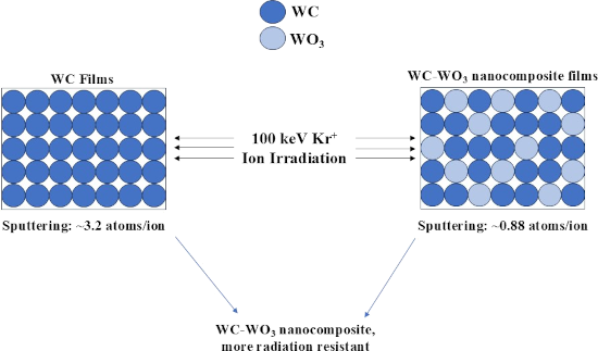
- experimental sputtering trends. Furthermore, preferential sputtering of lower-Z elements (C and O) was observed in both material systems. Glancing incidence X-ray diffraction analysis revealed post-irradiation grain growth in WC–WO3 films, while scanning electron microscopy results show morphological changes
- , Netherlands) in the 2θ range from 20° to 80°. Scanning electron microscopy measurements of pristine and irradiated S1 films were performed using a MIRA Tescan II SEM at a high voltage of 25 kV using detector working in secondary-emission mode. Results and Discussion Phase and compositional studies of the



Supramolecular one-dimensional conducting nanofibers from a C3-symmetric tetrathiafulvalene derivative
Beilstein J. Nanotechnol. 2026, 17, 872–881, doi:10.3762/bjnano.17.63
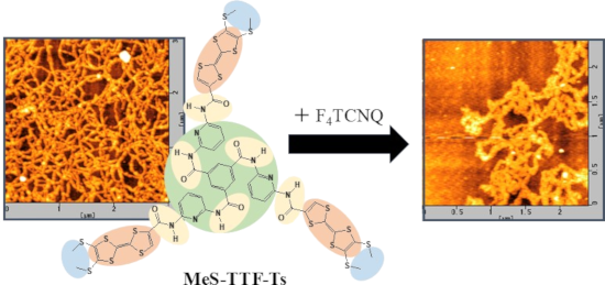
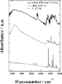
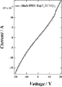
- marked differences in the observed morphologies. In addition to AFM observations, scanning electron microscopy (SEM) measurements were performed for representative samples deposited on HOPG substrates. Representative SEM images are provided in Supporting Information File 1 (Figures S2–S4). The


He+ FIBID-fabricated 3D AFM tip architectures: an exploratory study of hollow pillars, helices, and spirals
Beilstein J. Nanotechnol. 2026, 17, 863–871, doi:10.3762/bjnano.17.62
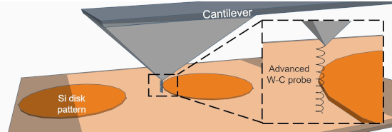
- examined by electron microscopy before and after AFM use. The main degradation modes were geometric deformation of the apex or shaft and mechanical fracture, most frequently at the tip–cantilever interface. While a few structures remained operational through repeated measurement cycles, others failed
- measurements from commercial reference probes serving as a step height baseline. Importantly, each printed structure was also inspected by electron microscopy before and after AFM use in order to document morphology changes, degradation pathways and architecture-dependent failure modes. In this way, the work
- tested conditions, confirming basic probe functionality, but without demonstrating any imaging advantage over commercial tips. The systematic before/after electron microscopy inspection shows that the dominant degradation modes are apex or shaft deformation and mechanical fracture, most frequently at the


Glycerol photoelectrochemical oxidation reaction at carbon nitrides/BiVO4 materials
Beilstein J. Nanotechnol. 2026, 17, 806–817, doi:10.3762/bjnano.17.57
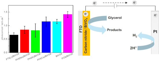
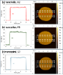
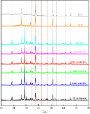
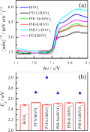
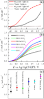
- acetylacetonate at 500 °C for 2 h. The CN/BiVO4 heterojunctions presented bandgap energy values, Eg, similar to pure BiVO4. X-ray diffraction analysis also revealed that the BiVO4 phase was not altered by the presence of the CN. However, scanning electron microscopy analysis coupled to energy-dispersive X-ray
- acquired from 10° to 80° at a rate of 2°·min−1 with a step size of 0.02°. Morphological features and elemental composition were determined by field-emission scanning electron microscopy (FEG-SEM; Zeiss Supra35) coupled with energy-dispersive X-ray spectroscopy (EDS), operating at 15 kV. Optical properties




Restorative potential of laser-synthesized silver nanoparticles with Salvia officinalis for periodontal disease treatment: an in vitro study
Beilstein J. Nanotechnol. 2026, 17, 781–795, doi:10.3762/bjnano.17.55
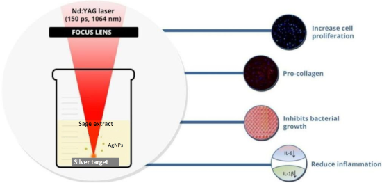
- . AgNPs were synthesized at two laser pulse energies (2 and 6 mJ), in sage extract and deionized water, and characterized by dynamic light scattering, transmission electron microscopy, and inductively coupled plasma optical emission spectroscopy. Synthesis at 6 mJ in sage extract (SageAgNPs6mJ) yielded
- polystyrene cuvettes (DTS0012, Malvern Panalytical, UK) at ambient temperature (25 ± 0.1 °C). The selected AgNPs that displayed antimicrobial effects were further analyzed by transmission electron microscopy (TEM), to evaluate their size, shape, and dispersity. An FEI Talos F200X microscope, operating at 200



Substrate-dependent pore formation in molybdenum disulfide monolayers under ion irradiation
Beilstein J. Nanotechnol. 2026, 17, 769–780, doi:10.3762/bjnano.17.54
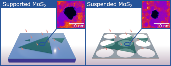
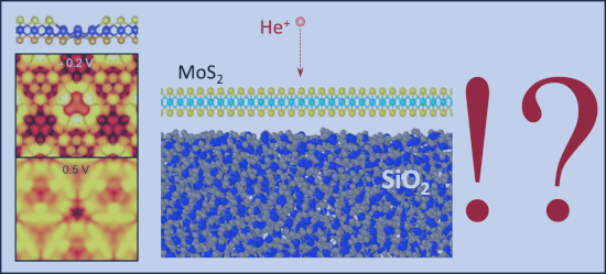
- highly charged ions (HCIs) and swift heavy ions (SHIs) – two types of ions that, despite having vastly different kinetic energies, both interact primarily with the electronic system of the target. Using scanning transmission electron microscopy, we quantify pore radii and pore formation efficiencies for
- under both HCI and SHI irradiation conclusively demonstrate the central role of substrate and interface-dependent electronic dissipation pathways regarding damage under these types of ion irradiation. Keywords: defects; MoS2; nanopores; SiO2; scanning transmission electron microscopy (STEM
- , high-resolution scanning transmission electron microscopy (STEM) generally requires freestanding membranes, while atomic-resolution atomic force microscopy (AFM) and scanning tunneling microscopy (STM) demand exceptionally clean surfaces; also, substrate effects can further complicate interpretation


Tailoring Ag–Pt nanoalloys through solid-state dewetting: structural and optical insights
Beilstein J. Nanotechnol. 2026, 17, 748–759, doi:10.3762/bjnano.17.52

- under an argon atmosphere. The process induced the transformation of continuous bilayers into isolated nanoislands through solid-state dewetting. Scanning electron microscopy and transmission electron microscopy analyses revealed the formation of well-defined, nearly spherical nanoislands with a
- a region with a lower film thickness at grain boundaries, which is well visible on the linear AFM profile in Figure 1 [45][46][47]. Figure 2a presents an exemplary scanning electron microscopy (SEM) image of nanostructures formed as a result of annealing of a silver–platinum bilayer with a thickness
- homogeneous Ag–Pt nanoalloys, high-resolution transmission electron microscopy (HR-TEM) observations were performed. Representative cross-section TEM images of two samples with various compositions are shown in Figure 8. Images for both nanostructures exhibit uniform morphology, which strongly indicates alloy




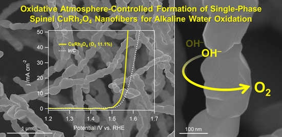
Oxidative atmosphere-driven formation of single-phase spinel CuRh2O4 nanofibers for alkaline water oxidation
Beilstein J. Nanotechnol. 2026, 17, 737–743, doi:10.3762/bjnano.17.50
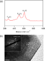
- 609.6 cm−1 (A1g), which are consistent with the spinel CuRh2O4 lattice [17][18], supporting the XRD-based phase assignment (vide supra). As shown in Figure 4b, high-resolution transmission electron microscopy (HRTEM) analysis of the electrospun CuRh2O4 nanofibers reveals clear lattice fringes with an
- electron microscopy (SEM) was employed to investigate the surface morphology and structural uniformity of the electrospun nanofibers after post-annealing. In the as-spun state prior to annealing, the fibers containing PVP exhibit smooth surfaces with an average diameter of approximately 300 nm (Supporting
- characterization Morphology and elemental composition of the synthesized nanomaterials were examined using field-emission scanning electron microscopy (FE-SEM; JEOL JSM-6700F) and high-resolution transmission electron microscopy (HRTEM; JEOL JEM-2100F). Surface chemical states and crystallographic structures were




Environmental applications of silver nanoparticles: state-of-the-art review and emerging trends
Beilstein J. Nanotechnol. 2026, 17, 697–736, doi:10.3762/bjnano.17.49
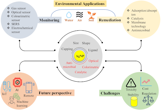
- needed before engineering AgNPs for particular applications. AgNPs are characterised using optical spectroscopy, electron microscopy, X-ray diffraction, and dynamic light scattering (DLS) to measure plasmonic absorbance, size, shape, structure, and stability [49]. Optical spectroscopy is a rapid and
- , which calculated the AgNP concentration as particles per millilitre [53]. Microscopic techniques, such as transmission electron microscopy, provide high-resolution images of individual nanoparticles, confirming morphology, size distribution, and elemental composition when coupled with energy-dispersive
- X-ray analysis [49]. TEM analysis is performed on copper grids with varying mesh sizes and coatings, with carbon/formvar-coated copper grids commonly preferred. Scanning electron microscopy (SEM) provides information on the silver nanoparticles’ surface properties and the aggregation state of dried


Molecular engineering of individual dye-based nanoparticle photostability for ultrabright two-photon fluorescence
Beilstein J. Nanotechnol. 2026, 17, 688–696, doi:10.3762/bjnano.17.48
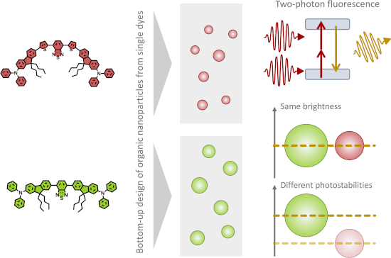
- ) Transmission electron microscopy (TEM) and size distribution of dFONs(1), data reused from [20]. (d) TEM and size distribution of dFONs(2). (e) Normalized absorption spectra of dFONs(1) (green) and dFONs(2) (red). (f) Normalized emission spectra of dFONs(1) (green) and dFONs(2) (red). (g) Two-photon absorption


Decontamination from water pollutants and pathogens by electrospun nanofibers doped with heavy-atom-free borafluorene-BODIPY photosensitizers
Beilstein J. Nanotechnol. 2026, 17, 668–682, doi:10.3762/bjnano.17.46
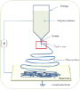
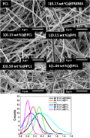
- 30 µm, Rotilabo®, Roth Selection, Germany), which was attached to the collector. After the electrospinning process, all mats were placed under a fume hood for 48 h to evaporate solvents in the fibers. Morphology analysis The morphological properties of samples were examined through scanning electron
- microscopy (SEM) using a JSM-6010PLUS/LV InTouchScope™ system from JEOL (Tokyo, Japan), operating at an accelerating voltage of 11 kV. Prior to imaging, each nonwoven sample underwent a double-coating process with a thin gold layer (2–3 nm). Microstructural analysis was subsequently performed utilizing



afspm: A framework for manufacturer-agnostic automation in scanning probe microscopy
Beilstein J. Nanotechnol. 2026, 17, 653–667, doi:10.3762/bjnano.17.45
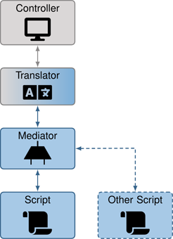
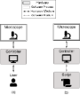
- instruments’ communication interfaces, and may benefit from similar frameworks. We particularly highlight optical and electron microscopy as these instruments share common experimental workflows (e.g., searching a wider region to determine where to image) and may benefit from direct repurposing of automation




Two-step laser synthesis of Ag@TiO2 nanomaterials for the photocatalytic degradation of rhodamine B
Beilstein J. Nanotechnol. 2026, 17, 622–634, doi:10.3762/bjnano.17.43
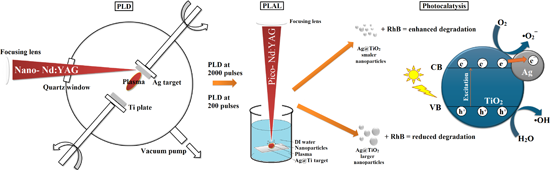
- characterization was performed using scanning electron microscopy (SEM) and transmission electron microscopy (TEM) with energy-dispersive spectroscopy (EDS), aiming to establish a clear correlation between synthesis parameters, nanostructure features, and photocatalytic activity. In our previous studies [6][7][21
- microstructural examination utilizing transmission electron microscopy. Investigations were conducted using scanning transmission electron microscopy, high-angle annular dark-field with energy-dispersive spectroscopy, and conventional and high-resolution transmission electron microscopy. A drop of the suspended


Recent progress in enhancing built-in electric fields of perovskite solar cells via junction engineering
Beilstein J. Nanotechnol. 2026, 17, 602–621, doi:10.3762/bjnano.17.42




Upcycling agroindustrial waste into graphene oxide supports for gold nanoparticles: toward sustainable nanomaterials
Beilstein J. Nanotechnol. 2026, 17, 489–504, doi:10.3762/bjnano.17.32
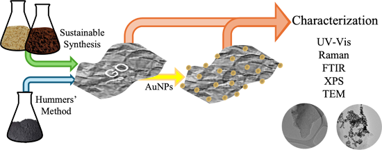
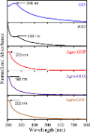
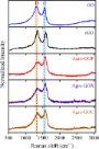
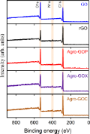
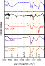
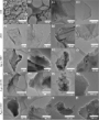
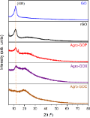
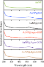
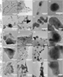
- = 1486.6 eV). The pass energy was set to 10 eV for high-resolution scans and to 40 eV for survey spectra. All binding energies were referenced to the C=C peak at 284.4 eV. Transmission electron microscopy (TEM) was carried using a JEOL JEM-2100 microscope operating at an accelerating voltage of 200 kV. TEM



Defects and defect-mediated engineering of two-dimensional materials: challenges and open questions
Beilstein J. Nanotechnol. 2026, 17, 454–488, doi:10.3762/bjnano.17.31
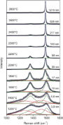
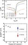
- created by impacts of energetic particles [18][19][20][21] by foreign atoms. Lots of insights into the structure and properties of defective 2D materials have been obtained using transmission electron microscopy (TEM), including conventional TEM and scanning TEM (STEM). These techniques, along with





Eco-efficient materials for agricultural crops based on a mineral rich in MOR- and HEU-type zeolites
Beilstein J. Nanotechnol. 2026, 17, 381–395, doi:10.3762/bjnano.17.26
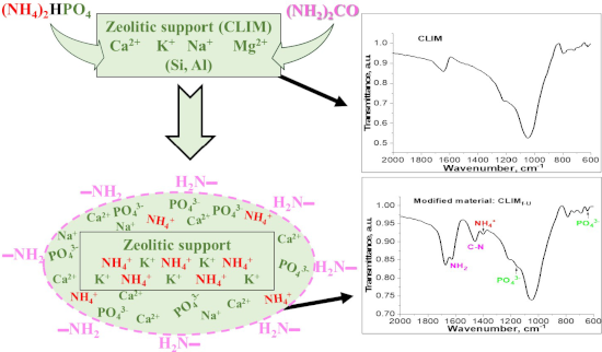
- urea arranged on the surface so that it covers the material and interacts with the zeolitic frameworks, was evidenced by Fourier-transform IR spectroscopy, adsorption measurements, scanning electron microscopy, scanning transmission electron microscopy, and other methods, as well as through culture
- microscopy (SEM), scanning transmission electron microscopy (STEM), N2 physisorption, and other research methods. Results and Discussion Characterization of DAP-modified zeolite CLIM The chemical compositions of natural zeolite (CLIM) from the San Andrés deposit and its modified forms (CLIMf) with ammonium
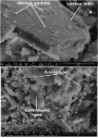
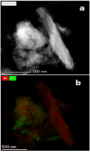
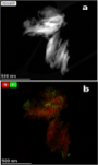
- consequence of the ion exchange processes (Equation 1) occurring during treatment of CLIM with DAP solution, which is in agreement with the data reported in [16][21][42]. Scanning electron microscopy and scanning transmission electron microscopy Microphotography (Figure 5) of natural zeolite (CLIM) revealed




Interconnection morphology effects on the radio frequency response of carbon nanotube sponges
Beilstein J. Nanotechnol. 2026, 17, 343–351, doi:10.3762/bjnano.17.23
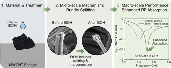
- . In particular, we observed that the response of S11 = −22.6 dB around 4.8 GHz from the CNS antenna improved after a mild treatment with ethanol, reaching S11 = −32.6 dB measured after 10 min of waiting. This observed effect is studied in detail with scanning electron microscopy and Raman spectroscopy
- findings point to a different interpretation related to the morphological effect of ethanol on the CNT mesh [27][29]. A scanning electron microscopy (SEM) study provided insights into the microstructure of the CNT film (Supporting Information File 1, Figure S1) and the sponges (Figure 3). The study



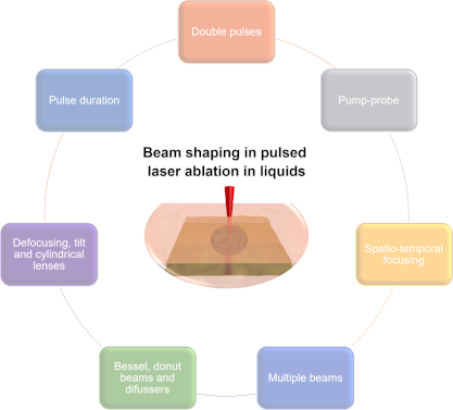
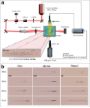
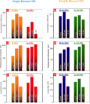
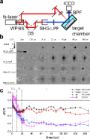
Beam shaping techniques for pulsed laser ablation in liquids: Unlocking tunable control of nanoparticle synthesis in liquids
Beilstein J. Nanotechnol. 2026, 17, 309–342, doi:10.3762/bjnano.17.22







Durable antimicrobial activity of fabrics functionalized with zeolite ion-exchanged nanomaterials against Staphylococcus aureus and Escherichia coli
Beilstein J. Nanotechnol. 2026, 17, 262–274, doi:10.3762/bjnano.17.18
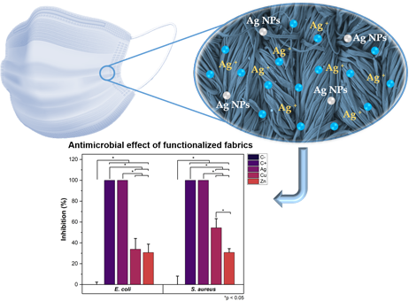
- atom % are evaluated regarding their antimicrobial activity against Staphylococcus aureus (Gram-positive) and Escherichia coli (Gram-negative), as well as regarding their physicochemical and mechanical properties. Scanning electron microscopy confirms the uniform distribution and successful
- ). Scanning electron microscopy confirmed the effective incorporation and uniform distribution of the nanomaterials on the fabric surface, facilitated by a 10% w/w acrylic resin binder. Among the tested materials, silver-based fabrics displayed the highest antibacterial efficacy, followed by copper and zinc
- , transmission electron microscopy (TEM) images were obtained using a JEOL JEM-2200FS (200 kV), and elemental analysis was performed using EDS. The crystalline structure of the modified fabrics was determined by X-ray diffraction (XRD) in a Panalytical AERIS diffractometer using Cu Kα (λ = 1.54184 Å). The