Search results
Search for "gap" in Full Text gives 671 result(s) in Beilstein Journal of Nanotechnology. Showing first 200.
Fe3O4 nanoparticles as a saturable absorber for giant chirped pulse generation
Beilstein J. Nanotechnol. 2019, 10, 1065–1072, doi:10.3762/bjnano.10.107

- 710119, China Hunan Key Laboratory of Super Microstructure and Ultrafast Process, School of Physics and Electronics, Central South University, Changsha and 410083, China 10.3762/bjnano.10.107 Abstract Fe3O4 nanoparticles (FONPs) are magnetic materials with a small band gap and have well-demonstrated
- ultrafast recovery time of 18–30 ps [3]. FONPs can be classified as a semiconductor material (with a band gap of ≈0.3 eV), which can be modulated by tuning the nanoparticle diameter [4]. For the magnetite (Fe3O4) material of anti-spinel structure, Fe(II) and Fe(III) of the octahedral position of the crystal


Electronic and magnetic properties of doped black phosphorene with concentration dependence
Beilstein J. Nanotechnol. 2019, 10, 993–1001, doi:10.3762/bjnano.10.100

- and high carrier mobility [7][8]. Unlike zero-band-gap graphene, the layer-dependent bandgap of black phosphorene ranges from 0.31 to 1.9 eV [9]. The hole-dominated mobility of phosphorene is up to 1000 cm2·V−1·s−1 theoretically [10], which is much higher than that of TMDs. These properties render
- of the supercell increases to 5 × 5, there is a gap of ca. 0.22 eV between the spin-up and spin-down energy bands near the Fermi level in the band structure of S-doped phosphorene, revealing a magnetic semimetal. Si-doped phosphorene also exhibits a semi-metallic state. The opened bandgap may be


Structural and optical properties of penicillamine-protected gold nanocluster fractions separated by sequential size-selective fractionation
Beilstein J. Nanotechnol. 2019, 10, 955–966, doi:10.3762/bjnano.10.96

- energies on nanocluster sizes indicates that the optical luminescence of the samples comes from the quantum confinement effect. The band gap of the NCs increases with a decrease in the dimension of the AuNC quantum structure. Conclusion In this research, a highly polydisperse penicillamine-protected AuNC


Synthesis of novel C-doped g-C3N4 nanosheets coupled with CdIn2S4 for enhanced photocatalytic hydrogen evolution
Beilstein J. Nanotechnol. 2019, 10, 912–921, doi:10.3762/bjnano.10.92

- attention because of the suitable band edge and band gap, as well as tunable optical properties [23][24][25][26][27][28]. For example, CdIn2S4 has been reported in various photoredox catalysis, such as organic photosynthesis, CO2 photoreduction and H2 evolution [29][30][31]. Despite these advances, the
- nanocomposites. It can be clearly observed that the light absorbance decreases in the visible light range upon addition of CdIn2S4 content in CISCCN nanocomposites. The band gap (Eg) of g-C3N4, CCN and CdIn2S4 can be estimated by plotting (αhν)2 as a function of the photon energy (Figure 6b), with α being the
- electrons on the hydrogen scale (about 4.5 eV), X is the electronegativity of the semiconductor, and Eg is the band gap energy of the semiconductor. The edge of the valence band (VB) and conduction band (CB) of g-C3N4, CCN and CdIn2S4 are summarized in Table 1. The separation–recombination rate of photo


Fabrication of silver nanoisland films by pulsed laser deposition for surface-enhanced Raman spectroscopy
Beilstein J. Nanotechnol. 2019, 10, 882–893, doi:10.3762/bjnano.10.89

- transfer) effect. In the CT mechanism the charge transfer between the molecules of the analyte and metallic nanostructures is excited, which leads to a resonant increase in the total EF. When the laser energy matches the energy gap between the HOMO and LUMO of molecules, a direct resonant Raman scattering


Rapid, ultraviolet-induced, reversibly switchable wettability of superhydrophobic/superhydrophilic surfaces
Beilstein J. Nanotechnol. 2019, 10, 866–873, doi:10.3762/bjnano.10.87

- heat treatment has been previously reported and was explained by the formation of Ti–O–H bonds under UV light, while heating of the surface results in the decrease in the concentration of Ti–O–H bonds [33][34]. As reported, due to the low band gap energy of TiO2, the photo-induced electron–hole pairs


Electronic properties of several two dimensional halides from ab initio calculations
Beilstein J. Nanotechnol. 2019, 10, 823–832, doi:10.3762/bjnano.10.82

- conduction-band minimum at the Γ point. Not surprisingly, the value of the bandgap obtained with the HSE functional is much larger than with the GGA. The values of the bandgap are 2.91 eV with GGA and 4.80 eV with HSE. BaFCl is found to be a direct-gap semiconductor with the valence-band maximum and the


Features and advantages of flexible silicon nanowires for SERS applications
Beilstein J. Nanotechnol. 2019, 10, 725–734, doi:10.3762/bjnano.10.72

- different gap sizes resulting in the lacunarity increase. The analysis of fractal dimension and lacunarity shows the results after water immersion are more separated from the dry sample than the results after ethanol immersion, indicating that water places the SiNWs closer together than EtOH. The smaller


The effect of translation on the binding energy for transition-metal porphyrines adsorbed on Ag(111) surface
Beilstein J. Nanotechnol. 2019, 10, 706–717, doi:10.3762/bjnano.10.70

- understanding the whole process. Since the energy depends almost linearly on the position for TM = (Cr, Fe, Co and Ni) it is reasonable to assume that in these cases the process will follow similar dynamics. For VPP, and partially for MnPP, a larger gap occurs between the “i” and “h” position, suggesting that


![[Graphic 1]](/bjnano/content/inline/2190-4286-10-70-i1.svg?max-width=637&scale=1.18182) , for all systems and relative molecule–surface positions. Right: symm...
, for all systems and relative molecule–surface positions. Right: symm...


![[Graphic 7]](/bjnano/content/inline/2190-4286-10-70-i7.svg?max-width=637&scale=1.18182) for selected TMPP systems (M = V, Mn, Co; red: positive values, blue: negative value...
for selected TMPP systems (M = V, Mn, Co; red: positive values, blue: negative value...
Self-assembly and wetting properties of gold nanorod–CTAB molecules on HOPG
Beilstein J. Nanotechnol. 2019, 10, 696–705, doi:10.3762/bjnano.10.69

- 4D. This value, however, does not reflect the true height of CTAB. This is due to convolution effects related to the inter-stripe gap (gap width ≈2.5 nm), which is much smaller than the radius of curvature of the AFM tip (≈8 nm). A more accurate estimation of the height of the CTAB stripes can be
- the gap width (≈2.5 nm), height (≈0.15 nm), and width (≈3 nm) of the residual striped features. (A) Schematic representation of a droplet containing CTAB-coated nanorods and a surplus of CTAB on the HOPG surface; the arrows indicate the relative evaporation rate of the solvent. (B) Hydrophobic HOPG


Outstanding chain-extension effect and high UV resistance of polybutylene succinate containing amino-acid-modified layered double hydroxides
Beilstein J. Nanotechnol. 2019, 10, 684–695, doi:10.3762/bjnano.10.68

- sweeps from 0.1 to 100 rad s−1 and the gap between plates set at 1 mm. In all cases, the oscillatory shear stress amplitude was checked to ensure that measurements were performed inside the linear viscoelastic domain. The storage modulus (G’), loss modulus (G”) and tan δ (ratio of G” and G’) were


Commercial polycarbonate track-etched membranes as substrates for low-cost optical sensors
Beilstein J. Nanotechnol. 2019, 10, 677–683, doi:10.3762/bjnano.10.67

- variations. Therefore, this study provides a new porous transducer adequate for the development of optical sensors. Results and Discussion Optical response of PCTE membranes: a Fabry–Pérot interferometer A FP interferometer is an optical structure consisting of two parallel reflective surfaces with a gap


A carrier velocity model for electrical detection of gas molecules
Beilstein J. Nanotechnol. 2019, 10, 644–653, doi:10.3762/bjnano.10.64

- variation of GNR energy band gap, and conversion of GNR to a n-type or p-type semiconducting material depending on whether it is an acceptor or donor functional molecule [21]. On the other hand, the variation of the energy band gap could convert the GNR properties from metallic to semiconducting, or vice
- carriers over the density of carriers, and is given by [26]: where is the magnitude of velocity (m is electron mass and Eg is energy band gap), and is the Fermi–Dirac distribution function that indicates the probability of occupation of a state at each energy level [27]. The DOS indicates the number of
- direction is obtained as: For the bare AGNR, the value of the hopping integral parameter is t′ = 0 eV. The value of the DOS near the Fermi level would be equal to 0 (eV)−1 for the bare AGNR and the width of zero DOS area should be equivalent to the energy band gap value of bare AGNR. This is because there


Review of time-resolved non-contact electrostatic force microscopy techniques with applications to ionic transport measurements
Beilstein J. Nanotechnol. 2019, 10, 617–633, doi:10.3762/bjnano.10.62

- build-up in the sample at the location of the AFM tip if an appropriate voltage is applied across the tip–sample gap. Measuring the resonance frequency shift as a function of time after the light is turned on/off then allows for the charging/discharging time to be directly acquired, revealing
- conducting materials as well. To probe ionic transport a step potential is applied between the AFM tip and a conducting back electrode, creating an electric field across the tip–sample gap and through the sample, illustrated in Figure 1b. The mobile ions inside the sample move in response to this field over


Temperature-dependent Raman spectroscopy and sensor applications of PtSe2 nanosheets synthesized by wet chemistry
Beilstein J. Nanotechnol. 2019, 10, 467–474, doi:10.3762/bjnano.10.46

- effect. Apart from this, these TMDCs, for example MoS2 and MoSe2, show an indirect to direct band gap transition [13][14][15][16][17]. A 2D platinum diselenide (PtSe2) material has recently joined the growing class of stable TMDCs due its promising applications. The 2D PtSe2 has not been explored much to
- date due to difficulties in synthesis. It is well known that bulk PtSe2 is a semimetal in nature with a nearly zero band gap [18][19]. With the help of theoretical calculations such as density functional theory (DFT) and local-density approximations (LDAs), it has been observed that bulk PtSe2 shows a
- semimetallic nature and single-layer PtSe2 has a semiconducting nature with a bandgap of 1.2 eV. Bilayer PtSe2 is also a semiconducting material but with a slightly smaller band gap than the monolayer material [19]. This layer-dependent conversion of semimetal-to-semiconductor transition has potential for


Reduced graphene oxide supported C3N4 nanoflakes and quantum dots as metal-free catalysts for visible light assisted CO2 reduction
Beilstein J. Nanotechnol. 2019, 10, 448–458, doi:10.3762/bjnano.10.44

- all these interesting properties, pure g-C3N4 only weakly absorbs visible light due to its wide band gap and also has poor electrical conductivity [18]. An efficient way to increase the charge separation and electrical conductivity of g-C3N4 is to modify it with rGO. Besides the structural and
- electron affinity (EEA) and first ionization (Eion) energy; Ee is the energy of free electrons on the hydrogen scale (≈4.5 eV vs NHE); Eg is the band gap of semiconductors. The conduction and valence band potential value for GCN-5 are −1.01 and 1.05 eV, respectively, and is found to be lower than any CN


Advanced scanning probe lithography using anatase-to-rutile transition to create localized TiO2 nanorods
Beilstein J. Nanotechnol. 2019, 10, 412–418, doi:10.3762/bjnano.10.40

- nanostructures. Keywords: hydrothermal crystal growth; lithography; nanostructures; seed crystals; surface processes; oxides; Introduction Rutile TiO2 is a chemically stable semiconductor with a band gap of 3.1 eV [1]. Dependent on the kind of nanostructure and doping, it has outstanding electronic and


Transport signatures of an Andreev molecule in a quantum dot–superconductor–quantum dot setup
Beilstein J. Nanotechnol. 2019, 10, 363–378, doi:10.3762/bjnano.10.36

- Hamiltonian H specified above is infinite-dimensional. However, if the temperature T is low and the superconducting gap Δ is large, then one may simplify the Hamiltonian by eliminating the superconducting quasiparticles from the description. Technically, this is done by integrating out the quasiparticles


Intuitive human interface to a scanning tunnelling microscope: observation of parity oscillations for a single atomic chain
Beilstein J. Nanotechnol. 2019, 10, 337–348, doi:10.3762/bjnano.10.33

- adatom, at a height corresponding to 0.4 μA tunneling current at 100 mV bias, which corresponds to a tunnel gap of 1.2 Å and around 250 kΩ tunnel resistance. Then, the tip is moved towards the adatom under feedback-off conditions while keeping Z constant. Similar to the jump to contact phenomenon that


Geometrical optimisation of core–shell nanowire arrays for enhanced absorption in thin crystalline silicon heterojunction solar cells
Beilstein J. Nanotechnol. 2019, 10, 322–331, doi:10.3762/bjnano.10.31

- ) of the NW array and thickness of supporting layers, the optimal NW dimensions were determined resulting in . It should be noted that an optimisation of the array periodicity could further improve the optical performance, particularly by choosing a value of Λ closer to the band-gap wavelength of c-Si


Site-specific growth of oriented ZnO nanocrystal arrays
Beilstein J. Nanotechnol. 2019, 10, 274–280, doi:10.3762/bjnano.10.26

- nanoscale optoelectronics [1][2][3][4]. ZnO is an important direct band gap (≈3.3 eV), nontoxic, metal oxide semiconductor, which can readily be used for optoelectronic applications. The properties of ZnO can be tailored by changing the morphology of the structures. Thus, fabrication of ZnO having different


Magnetic-field sensor with self-reference characteristic based on a magnetic fluid and independent plasmonic dual resonances
Beilstein J. Nanotechnol. 2019, 10, 247–255, doi:10.3762/bjnano.10.23
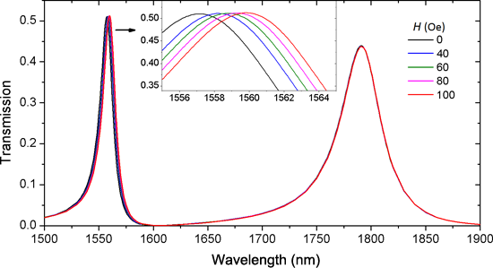
- theoretical analysis. When a disk is coupled to the upper stub 1, cavities modes can directly couple with each other through their evanescent field at small gap distances. When ω1 = ωd = ω, the transmittance of Equation 8 becomes T = |(κ1d + 1)/(κw1 + κ1d + 1)|2. This indicates that a transmission peak


Study of silica-based intrinsically emitting nanoparticles produced by an excimer laser
Beilstein J. Nanotechnol. 2019, 10, 211–221, doi:10.3762/bjnano.10.19

- material such as silica can significantly change the optical absorption spectrum [15][18][19]. Indeed, this can result in additional absorption bands [19] and/or change the band gap [18]. For example, it was suggested that for long-duration laser pulses, point defects can provide “seed” electrons for
- in the glass network and the addition of Ge decreases the silica band gap [18][21][22][23]. The presence of Ge is associated with the appearance of new structures of optically active point defects such as the so-called germanium lone pair center (GLPC) [19][24]. This defect is responsible for an
- , showing that for the used pure silica sample [31] a higher energy is needed. The acquired results confirm the positive role of the Ge doping, which facilitates the material removal by reducing the glass band gap and the presence of the Ge-related defects. By comparing the samples produced with different


Uniform Sb2S3 optical coatings by chemical spray method
Beilstein J. Nanotechnol. 2019, 10, 198–210, doi:10.3762/bjnano.10.18

- sulfide (Sb2S3), an environmentally benign material, has been prepared by various deposition methods for use as a solar absorber due to its direct band gap of ≈1.7 eV and high absorption coefficient in the visible light spectrum (1.8 × 105 cm−1 at 450 nm). Rapid, scalable, economically viable and
- environmentally benign material. As Sb and S are abundant elements in the Earth’s crust, enough raw materials can be supplied to manufacture large quantities of Sb2S3 in the long term. Sb2S3 can be applied as the inorganic absorber in solar cells due to its direct band gap of ≈1.7 eV [1][2]. Sb2S3, prepared by a
- -brown layers. Furthermore, in our previous paper, 250 °C was found to be too high a deposition temperature to obtain sufficient coverage of TiO2 substrate by polycrystalline Sb2S3 thin films, despite the suitable band gap of 1.6 eV and high phase purity [12]. Restricted to deposition temperatures in the


Amorphous NixCoyP-supported TiO2 nanotube arrays as an efficient hydrogen evolution reaction electrocatalyst in acidic solution
Beilstein J. Nanotechnol. 2019, 10, 62–70, doi:10.3762/bjnano.10.6

- heterojunction can lower the band gap of the material thus augment the conductivity. The material band gap can be calculated by measuring the optical absorption edge in UV–vis DRS, shown in Figure 5f. It is observed that the absorption edge showed a red shift after electrodeposition of Ni–P and NiCoP. The
- absorption edges are 398, 405, and 488 nm for TNAs, Ni–P/TNAS, and NixCoyP/TNAs, corresponding the band gaps of 3.12, 3.06, and 2.54 eV, respectively. Sample NixCoyP/TNAs had a band gap 0.52 eV lower than that of Ni–P/TNAs. This indicates that the binary-metal phosphides synthesized via electrodeposition


