


Search results
Search for "ion irradiation" in Full Text gives 58 result(s) in Beilstein Journal of Nanotechnology.
Nanoglasses: a trail towards uncharted regions of vitreous materials and their properties?
Beilstein J. Nanotechnol. 2026, 17, 1047–1062, doi:10.3762/bjnano.17.72
- structural heterogeneities in metallic glasses that have been processed by plastic (shear) deformation or, alternatively, that have been irradiated by ions with a high kinetic energy. Plastic shear deformation leads to extended plate-like shear bands [57], and ion irradiation causes rod-like ion tracks [33


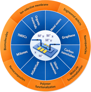
Materials challenges in solid-state sensors for continuous monitoring of ions in water
Beilstein J. Nanotechnol. 2026, 17, 935–973, doi:10.3762/bjnano.17.66


Enhanced erosion resistance and radiation stability of WC–WO3 nanocomposite films under 100 keV Kr+ ion irradiation
Beilstein J. Nanotechnol. 2026, 17, 922–934, doi:10.3762/bjnano.17.65
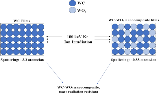
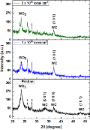
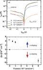
- potential ceramic-based PFC materials, specifically tungsten carbide (WC) thin films and their nanocomposite counterpart, WC–WO3, under 100 keV Kr+ ion irradiation. The films were irradiated at fluences of 1 × 10¹⁶, 3 × 10¹⁶, and 1 × 10¹⁷ ions/cm2. Rutherford backscattering spectrometry was employed to
- resilience to ion irradiation, reinforcing its potential as a radiation-resistant material in nuclear environments [13]. WO3, in contrast, has other advantages, including its capability to act as a radiation absorber and its chemical inertness [14][15][16]. However, hardness and toughness of the
- erosion in the composite thin films. Thus, the present work aims to investigate the erosion behaviour of WC–WO3 nanocomposite films and its comparison with WC films under “low-energy” ion irradiation, i.e., in the nuclear energy loss regime. It is important to note that the nuclear energy loss (Sn



Substrate-dependent pore formation in molybdenum disulfide monolayers under ion irradiation
Beilstein J. Nanotechnol. 2026, 17, 769–780, doi:10.3762/bjnano.17.54
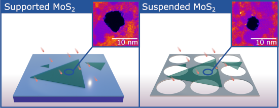
- Abstract Ion irradiation is a versatile tool for nanostructuring surfaces, yet the roles of energy deposition and dissipation at the surface and in ultrathin materials remain poorly understood. In this study, we investigate nanopore formation in monolayer MoS2 on different substrates under irradiation of
- under both HCI and SHI irradiation conclusively demonstrate the central role of substrate and interface-dependent electronic dissipation pathways regarding damage under these types of ion irradiation. Keywords: defects; MoS2; nanopores; SiO2; scanning transmission electron microscopy (STEM
- ); Introduction Ion beams provide a controllable route to engineer defects in two-dimensional (2D) materials, enabling property tuning from doping to nanopore formation [1][2][3][4]. Because kinetic energy, charge state, and mass can be varied over wide ranges, ion irradiation offers a large parameter space for


Defects and defect-mediated engineering of two-dimensional materials: challenges and open questions
Beilstein J. Nanotechnol. 2026, 17, 454–488, doi:10.3762/bjnano.17.31
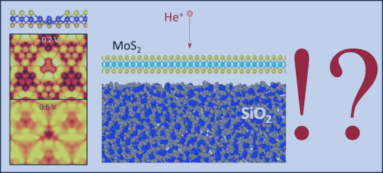
- distribution rather uniform. The average vacancy cluster size in Figure 9a is twelve vacancies. A similar mechanism of vacancy cluster self-organization applies to the moiré of h-BN with Ir(111) [157]. Figure 9d displays the pristine h-BN moiré with pronounced bright spots. Upon 500 eV He+ ion irradiation at





Evaluating metal-organic precursors for focused ion beam-induced deposition through solid-layer decomposition analysis
Beilstein J. Nanotechnol. 2025, 16, 1942–1951, doi:10.3762/bjnano.16.135
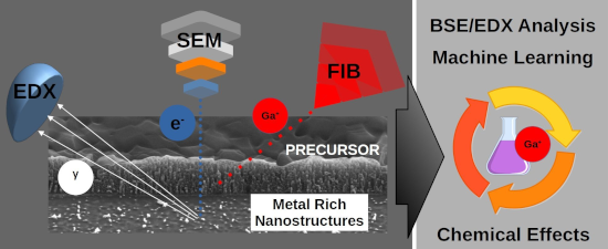
- . These studies also enabled a clear distinction between the processes occurring under ion irradiation and under electron irradiation. Furthermore, investigations on the gold complex [AuMe2(hfac)] have allowed for the assessment of the influence of ion type (mass) and ion energy on molecular decomposition
- occurs throughout ion irradiation, this point marks the transition beyond which further irradiation leads primarily to material removal rather than the structure growth. The structures formed at “the optimal” ion fluence were examined by scanning electron microscopy energy-dispersive X-ray spectroscopy
- layer has a rather homogeneously distributed chemical composition, and only a few low-contrast grooves are visible. During ion irradiation, the BSE contrast increases strongly already in the very early stages of bombardment. An increasing number of (“grid”) dark contrast grooves separating elongated


Electrical, photocatalytic, and sensory properties of graphene oxide and polyimide implanted with low- and medium-energy silver ions
Beilstein J. Nanotechnol. 2025, 16, 1794–1811, doi:10.3762/bjnano.16.123
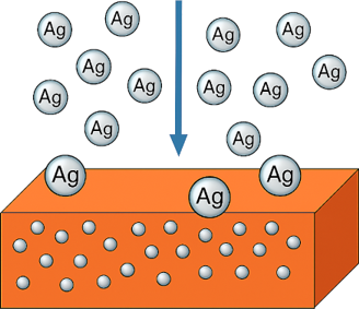
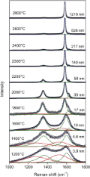
- structural analysis of GO before and after ion irradiation was conducted using Raman spectroscopy [28]. This spectroscopic technique, known for its effectiveness in probing disorders and defects within crystal structures, proved particularly valuable in characterizing graphite and its derivatives [29]. The
- the ID/IG ratio reaching values of 1.06, which is higher than in the previous case. Ag ion irradiation causes more defects in GO when 1.5 MeV energy ions were used. By comparing of the Figure 7a and Figure 7b, we can see that both ion fluences lead to a narrowing of the D and G bands with respect to
- unmodified GO. This narrowing can be induced by structural changes occurring in GO due to ion irradiation. Cracking and breakage of the internal structure of GO may be the most common cause of this profile narrowing [4]. The significant decrease in the intensity of the D peak at both implantation energies


Characterization of ion track-etched conical nanopores in thermal and PECVD SiO2 using small angle X-ray scattering
Beilstein J. Nanotechnol. 2025, 16, 899–909, doi:10.3762/bjnano.16.68
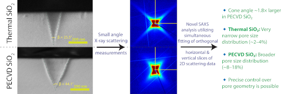
- nanopores in different materials, which is essential for optimizing membrane performance in applications that require precise pore geometry. Keywords: etched ion tracks; SiO2; small angle X-ray scattering (SAXS); swift heavy ion irradiation; track-etched nanopores; Introduction Solid-state nanopores have
- and a wider size distribution. Results and Discussions Figure 1 shows plan-view scanning electron microscopy (SEM) images of nanopores fabricated in thermal (Figure 1a) and PECVD (Figure 1b) SiO2 by etching ion tracks produced with 1.6 GeV Au ion irradiation (see Experimental and Theory section for
- variations in material properties. While thermal SiO2 typically exhibits high homogeneity in local material properties, factors such as the etching process and the ion irradiation energy straggling may introduce an effective narrow size distribution of pores. Although we apply a Schulz–Zimm distribution to


Focused ion and electron beams for synthesis and characterization of nanomaterials
Beilstein J. Nanotechnol. 2025, 16, 613–616, doi:10.3762/bjnano.16.47
- focused electron beam-induced etching (FEBIE), can effectively control edge profiles, supported by continuum modeling [12]. Additionally, using alternative precursors such as Pt(CO)2Cl2 and Pt(CO)2Br2 with low-energy ion irradiation enables the fabrication of high-purity Pt deposits. This process involves

Retrieval of B1 phase from high-pressure B2 phase for CdO nanoparticles by electronic excitations in CdxZn1−xO composite thin films
Beilstein J. Nanotechnol. 2025, 16, 551–560, doi:10.3762/bjnano.16.43

- as an effective tool. Exposure to 120 MeV silver ion irradiation results in the complete amorphization of the B2 phase in CdO nanoparticles, while the crystalline hexagonal wurtzite phase of zinc oxide (ZnO) remains intact. In contrast, 80 MeV oxygen ion irradiation preserves the B2 phase and
- facilitates the reemergence of the B1 phase. The partial damage caused by electronic energy loss during oxygen ion irradiation in the willemite Zn2SiO4 phase is identified as a trigger for the B1 to B2 phase transformation in CdO nanoparticles, enabling the recovery of the B1 phase. The diminishing local
- pressure exerted by the Zn2SiO4 phase on CdO nanoparticles during oxygen ion irradiation leads to the coexistence of both B1 and B2 phases. X-ray absorption near-edge spectra (XANES) reveal minimal changes in the intensity of the spike-like Zn L3,2 pre-edge feature associated with the Zn2SiO4 phase under


N2+-implantation-induced tailoring of structural, morphological, optical, and electrical characteristics of sputtered molybdenum thin films
Beilstein J. Nanotechnol. 2025, 16, 495–509, doi:10.3762/bjnano.16.38
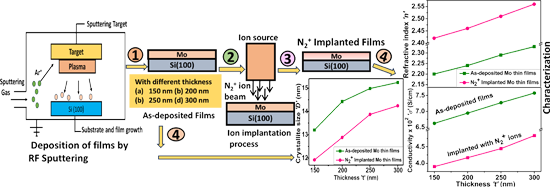
- ][20][21]. Ahmed et al. [13] investigated the effect of helium ion irradiation on the structural and electrical properties of Mo thin films. They noted that α-particles create defects that reduce charge carrier mobility, and the hardness increased from low to high ion fluence. Hoffman et al. [14
- accelerating voltage. At grazing incidence, the observed stress is either minimal or slightly tensile and is mostly unaffected by the accelerating voltage. Tripathi et al. [18] examined the temperature-dependent surface alterations in Mo films induced by He+ ion irradiation within the 773–1073 K range as a
- polycrystalline Mo mirrors for plasma diagnostics when treated with low-energy He+ ion irradiation at ambient temperature and 400 °C. Takamura et al. [21] examined the effects of He plasma irradiation on Mo thin films. The temperature range for nanostructure growth was within a temperature range of 800 to 1050 K


Performance optimization of a microwave-coupled plasma-based ultralow-energy ECR ion source for silicon nanostructuring
Beilstein J. Nanotechnol. 2025, 16, 484–494, doi:10.3762/bjnano.16.37

- impurities, and the effect of chemical compound formation and compound ion irradiation [44][45]. In cases of ultralow-energy ion bombardment, the rate of sputtering is lower compared to medium-energy ion bombardment; therefore, in this case, mass redistribution of the surface atoms plays a key role. There is


Effect of radiation-induced vacancy saturation on the first-order phase transformation in nanoparticles: insights from a model
Beilstein J. Nanotechnol. 2024, 15, 1453–1472, doi:10.3762/bjnano.15.117

- film through in situ ion irradiation, observed using atomic-resolution transmission electron microscopy [16]. The gold sample was irradiated with 2.8 MeV Au4+ ions at 200 °C with a fluence of approximately 1014 ions·cm−2 (equivalent to a dose of 10 dpa). A combination of surface- and radiation-induced
- et al. used transmission electron microscopy to investigate nanoscale Pd under 240 keV Kr ion irradiation with a flux of 1013 ions·cm−2·s−1. Pd had grain sizes, d, ranging from 10 to 100 nm. The authors found that the defect density increases with increasing grain size d, and the slope between defect


Ion-induced surface reactions and deposition from Pt(CO)2Cl2 and Pt(CO)2Br2
Beilstein J. Nanotechnol. 2024, 15, 1427–1439, doi:10.3762/bjnano.15.115

- ion irradiation these PtCl2 or PtBr2 species experience ion-induced sputtering. The difference between halogen and Pt sputter rates leads to a critical ion dose at which only Pt remains in the film. A comparison of the different ion/precursor combinations studied revealed that this sequence of
- ion beam. For Pt deposits, although MeCpPtMe3 meets the volatility and stability requirements, the inability to directly desorb the cyclopentadienyl ligands results in significant carbon contamination upon ion irradiation [21]. Alternatives to the carbon-rich MeCpPtMe3 complex are the four coordinate
- where a substrate at room temperature is exposed to a constant flux of Pt(CO)2Cl2 molecules and Ar+ ions. Results The mass spectra in Figure 1 identify the volatile species produced from Ar+ ion irradiation of Pt(13CO)2Cl2. The UHV chamber background gases (H2, H2O, and 12CO/N2) and Ar (Ar2+, m/z 20; Ar



Unveiling the nature of atomic defects in graphene on a metal surface
Beilstein J. Nanotechnol. 2024, 15, 416–425, doi:10.3762/bjnano.15.37
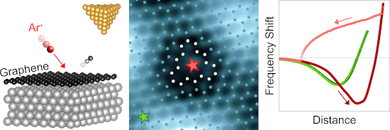
- by noble-gas ion irradiation [6][13][14][17][19][21][24], represents an opportunity for systematic defect studies. The work presented here was stimulated by the lack of experimental data on the actual geometry of atomic-scale defects in graphene. So far, scanning tunneling microscope (STM


Investigating ripple pattern formation and damage profiles in Si and Ge induced by 100 keV Ar+ ion beam: a comparative study
Beilstein J. Nanotechnol. 2024, 15, 367–375, doi:10.3762/bjnano.15.33
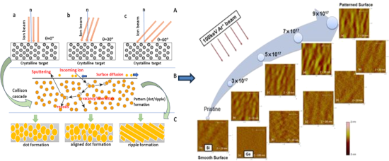
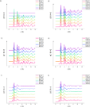
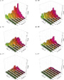
- earlier reports suggested that Ge is resistant to structural changes upon Ar+ ion irradiation, in the present case, a ripple pattern is observed on both Si and Ge. The irradiated Si and Ge targets clearly show visible damage peaks between channel numbers (1000–1100) for Si and (1500–1600) for Ge. The
- chosen from the literature [37][38] as 3, 5, 7, and 9 × 10¹⁷ ions/cm2 to induce complete amorphization within the two surfaces up to the ion range. The ion irradiation experiment was performed in the 90-degree beam line dedicated for materials science experiments in the Low-Energy Ion Beam (LEIB
- analysis of Si and Ge samples irradiated with a fluence of 9 × 10¹⁷ ions/cm2 was performed in cross-sectional mode. The TEM image clearly reveals the surface modification occurred due to Ar ion irradiation. At fewer places, Ar bubbles of ≈15 nm were also visible (marked with a dotted section) in Si. It was


Ion beam processing of DNA origami nanostructures
Beilstein J. Nanotechnol. 2024, 15, 207–214, doi:10.3762/bjnano.15.20
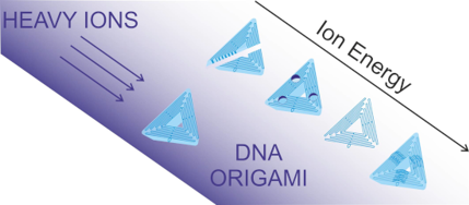
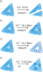
- by ion beams, modeling ion implantation, lithography, and sputtering conditions. Structural changes in 2D DNA origami nanostructures deposited on Si are analyzed using AFM imaging. The observed effects on DNA origami include structure height decrease or increase upon fast heavy ion irradiation in
- vacuum and in air, respectively. Slow- and medium-energy heavy ion irradiation results in the cutting of the nanostructures or crater formation with ion-induced damage in the 10 nm range around the primary ion track. In all these cases, the designed shape of the 2D origami nanostructure remains
- common type of beam processing, namely focused ion beam technology (FIB). Following the results of high- and medium-energy ion irradiation on deposited DNA origami nanostructures, which will be presented in this work, we wanted to explore whether we could observe similar effects using a commonly used


Ultralow-energy amorphization of contaminated silicon samples investigated by molecular dynamics
Beilstein J. Nanotechnol. 2023, 14, 834–849, doi:10.3762/bjnano.14.68
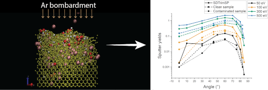
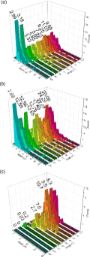
- conditions for contaminant removal. Sample purity is also enhanced since fewer argon atoms are implanted into the sample. This hypothesis regarding contamination removal will be confirmed in the section on the sputtering yields. Sputtering yield The sputtering yield in ion irradiation experiments is




Influence of water contamination on the sputtering of silicon with low-energy argon ions investigated by molecular dynamics simulations
Beilstein J. Nanotechnol. 2022, 13, 986–1003, doi:10.3762/bjnano.13.86
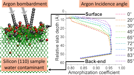
- extreme cases. Nowadays, very little is known about the influence of contaminations on the amorphization process under ion irradiation. Thanks to molecular dynamics (MD) simulations, a wide range of materials properties and process parameters can be reproduced [27][28][29]. In this paper, we are using MD
- cascade happened and to increase it after the energy dissipated into the system. During the ion irradiation simulations, the bottom slab of the sample (one lattice high) was set in an NVT ensemble using the same methodology in order to reproduce a heat-bath effect [55]. The remaining atoms were kept in
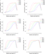
- (iii) the crystalline region, which remains unaffected underneath by ion irradiation. Closer to grazing incidence (e.g., above 75°), argon implantation becomes sparse; however, fragmentation and sputtering of water molecules reach maximum values. Hence, sputtering yields and molecular fragmentation




A broadband detector based on series YBCO grain boundary Josephson junctions
Beilstein J. Nanotechnol. 2022, 13, 325–333, doi:10.3762/bjnano.13.27
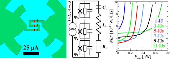
- deposition of YBaCuO films on a bicrystal substrate [25]. This problem can be mitigated by using ion irradiation [4][18][26] or step-edge junction technology [19], which will significantly increase the receiving properties and efficiency of the JJ series at high frequencies. While the integral received power



Is the Ne operation of the helium ion microscope suitable for electron backscatter diffraction sample preparation?
Beilstein J. Nanotechnol. 2021, 12, 965–983, doi:10.3762/bjnano.12.73
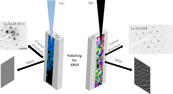
- values throughout the work against which the ion-irradiation-induced effects are evaluated. All values can be found in Table 1. Non-irradiated copper: electropolishing and Ar ion polishing To evaluate the effect of electropolishing and argon ion polishing on EBSD measurements, the Cu sample was polished
- challenging stress/strain analysis. Irradiation of copper at 0° incidence angle To assess the effect of ion irradiation, the copper TEM lamella grids were irradiated with Ga ions using a Ga FIB/SEM or Ne ions using HIM. An ion dose of 3371 ions/nm2 was chosen to allow a comparison with a previously reported
- study on Ga-induced phase transformations in copper [34]. A lower ion dose (2247 ions/nm2) was also evaluated as it corresponds to the dose that is achieved for commonly reported EBSD polishing time values over larger areas [39]. 30 keV Ga ion irradiation at 0° incidence angle The ion trajectory plot



A review of defect engineering, ion implantation, and nanofabrication using the helium ion microscope
Beilstein J. Nanotechnol. 2021, 12, 633–664, doi:10.3762/bjnano.12.52
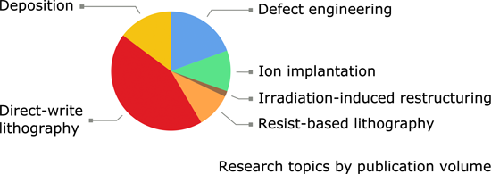
- applications using the highest doses (many orders of magnitude higher than the largest dose shown in Figure 1c) are milling and gas-assisted ion beam-induced deposition. Review 1 Defect engineering The use of the HIM as a source of localized helium ion irradiation with which to tune material properties through
- nanoscale regions. Several other studies of selective helium ion-induced conductivity changes in graphene have also been conducted [23] and a theoretical treatment of defect-induced conductivity changes upon helium ion irradiation of free-standing compared to supported monolayer graphene can be found in [24
- ]. Various 2D transition metal dichalcogenides have also been the subject of conductivity-tuning studies in the HIM. For example, Fox et al. showed that site-selective helium ion irradiation, introducing point defects and local disorder, transformed targeted regions of a supported pristine few-layer MoS2


The patterning toolbox FIB-o-mat: Exploiting the full potential of focused helium ions for nanofabrication
Beilstein J. Nanotechnol. 2021, 12, 304–318, doi:10.3762/bjnano.12.25
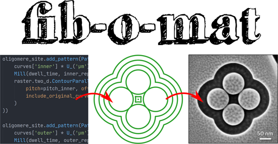
- -based devices encoding bits using nanoscale domain walls or skyrmions [4]. The magnetic properties of thin magnetic films and multilayers can directly be modified in a controlled manner by low-dose ion irradiation. Local variation of the dose using masks or focused ion beams leads to pure magnetic
- opposite out-of-plane magnetization in remanence. We are particularly interested in how ion irradiation changes the morphology of the magnetic domains and how it influences the nucleation and annihilation of domains in a typical adiabatic field cycle as well as after picosecond laser excitation [37][38


Bio-imaging with the helium-ion microscope: A review
Beilstein J. Nanotechnol. 2021, 12, 1–23, doi:10.3762/bjnano.12.1
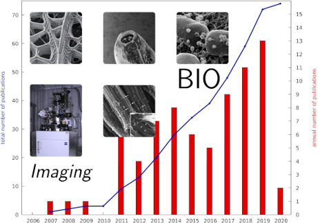
- lower than 1014 ions·cm−2. However, lanthanide-doped nanoparticles proved to be relatively stable against the ion irradiation and seem to be promising materials for biomarkers to be used with the HIM. Later, Mi developed a particle-accelerator-based setup with high-energy protons and alpha particles to


Out-of-plane surface patterning by subsurface processing of polymer substrates with focused ion beams
Beilstein J. Nanotechnol. 2020, 11, 1693–1703, doi:10.3762/bjnano.11.151
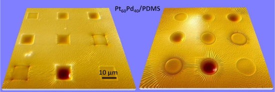
- -plane features, at the nanoscale, of the pre-deposited films. Ion irradiation of the Au-coated samples results in delamination, bulging, and perforation of the Au film, which is attributed to the accumulation of gases from radiolysis at the film–substrate interface. The irradiation with Ne+ and Ga+ ions
- the PMMA polymer under ion irradiation [5][6][7]. The most important physical and chemical phenomena behind this material modification include scission and cross-linking of polymer chains, which can occur simultaneously, as well as the formation of volatile molecules and their desorption from the
- been directed by their diverse applications in micro- and nanotechnology and by the high susceptibility of their structure to ion irradiation [5]. Another important aspect is that the chosen materials are different in their chemical structure, chemical composition, and mechanical properties. This is





