Search results
Search for "nanostructure" in Full Text gives 366 result(s) in Beilstein Journal of Nanotechnology. Showing first 200.
Determination of the radii of coated and uncoated silicon AFM sharp tips using a height calibration standard grating and a nonlinear regression function
Beilstein J. Nanotechnol. 2023, 14, 1200–1207, doi:10.3762/bjnano.14.99

- measured using a tip characterizer and tip qualification or standard calibration grating. In one of those studies, the tip geometry was determined by using a well-known sharp-edged silicon structure, which included height patterns with a certified pitch on a nanostructure plate [10]. Three types of AFM
- mode with very light loading (0.01 nN) to prevent the tips from wear. The noise effect was not considered here, because the measurement was conducted inside the hood of a MFP-3D Origin (Asylum Research) with noise filter system. Considering the geometry of the nanostructure and the scanline signal


A combined gas-phase dissociative ionization, dissociative electron attachment and deposition study on the potential FEBID precursor [Au(CH3)2Cl]2
Beilstein J. Nanotechnol. 2023, 14, 1178–1199, doi:10.3762/bjnano.14.98


Hierarchically patterned polyurethane microgrooves featuring nanopillars or nanoholes for neurite elongation and alignment
Beilstein J. Nanotechnol. 2023, 14, 1157–1168, doi:10.3762/bjnano.14.96

- , the question arises: Can discrete structures be combined with continuous structures for possible synergistic effects? Indeed, several studies have fabricated hierarchical discrete nanostructures on continuous microstructures in order to better mimic the micro- and the nanostructure of the native nerve
- ), indicating dominance of the nanostructure properties in this direction. In contrast, the CA values were higher and remained quite close to each other in magnitude even after O2 plasma treatment, signifying the dominance of the microgroove properties in this orientation. Despite the relatively high CA


Density functional theory study of Au-fcc/Ge and Au-hcp/Ge interfaces
Beilstein J. Nanotechnol. 2023, 14, 1093–1105, doi:10.3762/bjnano.14.90

- candidate for the observed nanostructure. However, a detailed analysis of the scattered intensity of atomic columns [23] suggests that the rows of Au atoms are located directly above the rows of Ge atoms. We therefore built variant D of the heterostructure, with 102 atoms (42 Ge and 60 Au), and the


Properties of tin oxide films grown by atomic layer deposition from tin tetraiodide and ozone
Beilstein J. Nanotechnol. 2023, 14, 1085–1092, doi:10.3762/bjnano.14.89

- have been studied from many perspectives. For example, one can mention anodes for Li-ion batteries [1], gas sensors [2], catalytic activities [3], and stable buffer [4] or base [5] layers in solar cells. More applications can be found, when SnO2 is considered as constituent of a nanostructure or a


Exploring internal structures and properties of terpolymer fibers via real-space characterizations
Beilstein J. Nanotechnol. 2023, 14, 1004–1017, doi:10.3762/bjnano.14.83

- through real-space mapping. Complementing these full-fiber scans, high-resolution topography and stiffness maps on smaller fiber subdomains were also obtained to study the nanostructure of Technora®. From detailed topography maps, we found that the well-aligned surface features observed on the full
- findings provide quantitative details about the branched network of fibrils that defines the nanostructure of Technora®. Technora® vs Kevlar® K29 To further highlight the unique internal nanostructure of Technora®, we compare topography and stiffness maps of Technora® to the more widely studied Kevlar® K29
- contextualize several aspects related to our findings. First, we describe how this real-space characterization provides new information about the Technora® fiber nanostructure. We then focus on fiber microstructures, highlighting how this technique expands upon conclusions from previous studies. Lastly, we


Prediction of cytotoxicity of heavy metals adsorbed on nano-TiO2 with periodic table descriptors using machine learning approaches
Beilstein J. Nanotechnol. 2023, 14, 939–950, doi:10.3762/bjnano.14.77

- interpret and can be calculated quickly without the involvement of expert personnel. These descriptors simplify the nanostructure property calculation and determine the nanoscale interactions without much computational intervention. The use of such descriptors saves time; the descriptors are also cost


Biomimetics on the micro- and nanoscale – The 25th anniversary of the lotus effect
Beilstein J. Nanotechnol. 2023, 14, 850–856, doi:10.3762/bjnano.14.69

- paper “The origin of black and white coloration of the Asian tiger mosquito Aedes albopictus (Diptera, Culicidae)” analysed the reflectance spectra of the white scales as well as the micro- and nanostructure of the black and white scales on the tarsi of A. albopictus. The results show that the white
- colour is produced by the hierarchical micro- and nanostructure of the surface. The reflection of light depends on the angle of incidence. In addition to superhydrophobicity, these results suggest that the scales have another function – their hierarchical structures produce the brilliant white colour


Investigations on the optical forces from three mainstream optical resonances in all-dielectric nanostructure arrays
Beilstein J. Nanotechnol. 2023, 14, 674–682, doi:10.3762/bjnano.14.53

- within the confined fields of three optical resonances supported by all-dielectric nanostructure arrays, including toroidal dipole (TD), anapoles, and quasi-bound states in continuum (quasi-BIC) resonances. By elaborately designing the geometry of a slotted-disk array, three different resonances can be
- large contrast in the optical forces generated with these resonances is attributed to a higher electromagnetic field enhancement provided by the quasi-BIC. These results suggest that the quasi-BIC resonance is preferred when one employs all-dielectric nanostructure arrays for the trapping and
- , these resonances by the spheres are beyond the spectrum of our interest. The presence of PS spheres only leads to some spectral shift of the resonances supported by the silicon nanostructure, which have been fully considered. Using the Maxwell stress tensor (MST) technique [17], the generated optical


Metal-organic framework-based nanomaterials as opto-electrochemical sensors for the detection of antibiotics and hormones: A review
Beilstein J. Nanotechnol. 2023, 14, 631–673, doi:10.3762/bjnano.14.52

- ), impurity-induced defects, or it may exist in pure crystals or molecules. According to the manner of the substance excitation, several distinct forms of luminescence are differentiated, as shown in Figure 6. A molecule, nanostructure, or atom must be able to absorb light radiation, resulting in electronic


Thermal transport in kinked nanowires through simulation
Beilstein J. Nanotechnol. 2023, 14, 586–602, doi:10.3762/bjnano.14.49

- , the conductance is not monotonically decreasing. To explain the increase in conductance for angles beyond 20°, we must consider that the thermal transport in a nanostructure may differ when travelling along orientations of a crystalline lattice different from the [100] direction. Though the thermal
- conductivity of a theoretical crystal with cubic symmetry is isotropic (and investigations of perfectly cubic systems have found such [37]), because of the limited dimensions of a nanostructure along certain crystal axes the contribution to thermal transport in the lattice can be anisotropic. In addition


Observation of multiple bulk bound states in the continuum modes in a photonic crystal cavity
Beilstein J. Nanotechnol. 2023, 14, 544–551, doi:10.3762/bjnano.14.45

- . Such a periodic nanostructure array supports a BIC around 1.56 μm and has an infinite Q factor at the Г point, as shown in Figure 1b and Figure 1c, respectively. The electric field (E field) distribution of the eigenmode is shown in the inset of Figure 1b, and the white arrows indicate the in-plane E


The origin of black and white coloration of the Asian tiger mosquito Aedes albopictus (Diptera: Culicidae)
Beilstein J. Nanotechnol. 2023, 14, 496–508, doi:10.3762/bjnano.14.41

- ; insects; nanostructure; scales; structural white; Introduction Body color (coloration) and light signals (bioluminescence) have a fundamental role in insect inter- and intra-specific visual communication allowing for species recognition, mating, prey capture, and predator avoidance [1]. Insect colours


Conjugated photothermal materials and structure design for solar steam generation
Beilstein J. Nanotechnol. 2023, 14, 454–466, doi:10.3762/bjnano.14.36

- on conjugated organic materials. Conjugated organic materials are processed into fibers, membranes, and porous structures. Therefore, nanostructure design based on the concept of nanoarchitectonics is crucial to achieve high SSG efficiency. We discuss the considerations for designing SSG absorbers


Evaluation of electrosynthesized reduced graphene oxide–Ni/Fe/Co-based (oxy)hydroxide catalysts towards the oxygen evolution reaction
Beilstein J. Nanotechnol. 2023, 14, 420–433, doi:10.3762/bjnano.14.34
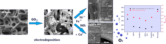
- nanostructure of CoNiFe and some agglomerations of GO microflakes, which was not the case for GO and CoNiFe alone (Figure 1b and Figure 1d, respectively). A difference was observed for NiFe-GO, that is, the morphology of GO and NiFe remained virtually the same after the combination of the catalysts. Another


Plasmonic nanotechnology for photothermal applications – an evaluation
Beilstein J. Nanotechnol. 2023, 14, 380–419, doi:10.3762/bjnano.14.33

- controlled due to extremely localised heating [38]. For increasing the spatial distribution of the generated heat, compared to an individual nanoparticle, nanoparticle assemblies and/or increased interfaces (by including constructions such as holes and other scattering centres) within a single nanostructure


Bismuth-based nanostructured photocatalysts for the remediation of antibiotics and organic dyes
Beilstein J. Nanotechnol. 2023, 14, 291–321, doi:10.3762/bjnano.14.26

- promising green and sustainable wastewater treatment method for a cleaner environment. Due to their narrow bandgaps, distinctive layered structures, plasmonic, piezoelectric and ferroelectric properties, and desirable physicochemical features, bismuth-based nanostructure photocatalysts have emerged as one
- static electric field, which effectively aids in the separation and transfer of photogenerated carriers. Bulk Bi and Bi-based nanostructure morphologies can also be easily altered using a variety of synthesis techniques due to their unique electrical and optical properties, which are directly tied to the
- plasmonic and photocatalytic properties. The typical and most recently applied bismuth-based nanostructure photocatalysts are depicted in Figure 2. Structural, optoelectronic, and magnetic properties Bismuth's peculiar optical, electronic, and more recently discovered photocatalytic and plasmonic properties


Atmospheric water harvesting using functionalized carbon nanocones
Beilstein J. Nanotechnol. 2023, 14, 1–10, doi:10.3762/bjnano.14.1

- occurs due to the presence of hydrophilic sites at the nanocone entrance. The functionalization, together with the high mobility of water inside nanostructures, leads to a fast water flow through the nanostructure. We show using molecular dynamics simulations that this device is able to collect water if


Electrical and optical enhancement of ITO/Mo bilayer thin films via laser annealing
Beilstein J. Nanotechnol. 2022, 13, 1589–1595, doi:10.3762/bjnano.13.133

- by many factors, such as the type of substrate [15], the deposition technique [16][17][18], the deposition conditions [19][20][21][22], and the annealing treatment [23]. Among these factors, heat treatment is a significant factor in rearranging the nanostructure, removing defects, and improving the
- size increased with the laser energy up to 200 mJ. It decreased to reach a minimum at an energy of 240 mJ. This trend in crystallite size is due to the rearrangement of the nanostructure. The particles sizes increase, defects are reduced, and the dislocation density (δ) decreases from 6.53 × 10¹⁴ to


Recent trends in Bi-based nanomaterials: challenges, fabrication, enhancement techniques, and environmental applications
Beilstein J. Nanotechnol. 2022, 13, 1316–1336, doi:10.3762/bjnano.13.109

- semiconductor surface. SPRs can potentially boost quantum yield by broadening the spectral response range of semiconductors. Fe, Au, Co, Ag, Ni, Bi, Al, and other metallic elements are often deposited and doped. For example, a nanostructure composite based on plasmonic Ag metal nanoclusters and monoclinic BiVO4


Enhanced electronic transport properties of Te roll-like nanostructures
Beilstein J. Nanotechnol. 2022, 13, 1284–1291, doi:10.3762/bjnano.13.106

- work, the electronic transport properties of Te roll-like nanostructures were investigated in a broad temperature range by fabricating single-nanostructure back-gated field-effect-transistors via photolithography. These one-dimensional nanostructures, with a unique roll-like morphology, were produced
- charges have been studied in p-type Te NBs [13]. In this work, we have studied the electronic transport properties of a distinct one-dimensional t-Te nanostructure with a roll-like morphology, which resembles cinnamon sticks. The nanostructures were obtained by a facile PVP-assisted hydrothermal route
- -nanostructure back-gate FETs, as well as the electrical resistivity of the nanostructures as a function of temperature from 5 to 400 K. The transport measurements were carried out in a low-noise custom-made system for electrical characterization of FET devices [16][17][18]. FET devices were built by laser


Laser-processed antiadhesive bionic combs for handling nanofibers inspired by nanostructures on the legs of cribellate spiders
Beilstein J. Nanotechnol. 2022, 13, 1268–1283, doi:10.3762/bjnano.13.105

- special fingerprint-like surface nanostructure. In this work, we present a theoretical model of the interaction of linear nanofibers with a sinusoidally corrugated surface. This model allows for a prediction of the adhesive interaction and, thus, the design of a suitable surface structure to prevent
- metatarsus of the hindmost (fourth) legs [10] (Figure 1). The 10–30 nm thick silk nanofibers do not stick to the calamistrum due to a special fingerprint-like nanostructure. This was characterized recently [14] for the calamistrum of Uloborus plumipes (commonly named feather-legged lace weaver or the garden
- nanostructure on the calamistrum in fact reduces adhesion of native spider silk and that this reduced adhesion can be mimicked by artificially structured polymer foils [14]. In order to technically integrate these antiadhesive structures, the structures have to be adapted as typical technical nanofibers differ


Studies of probe tip materials by atomic force microscopy: a review
Beilstein J. Nanotechnol. 2022, 13, 1256–1267, doi:10.3762/bjnano.13.104

- of the internal Pd nanowires will help probe more surface conductivity measurement, the nanowires with nanostructure or form good ohmic contact to the characterization of surface, external carbon nanotubes provide higher mechanical stability, can make the probe after many times of measuring still

Design of surface nanostructures for chirality sensing based on quartz crystal microbalance
Beilstein J. Nanotechnol. 2022, 13, 1201–1219, doi:10.3762/bjnano.13.100

- QCM system, which include organic molecules, supermolecular assemblies, inorganic nanostructures, and metal surfaces. The sensing mechanisms based on these surface nanostructures and the related potentials for chiral detection by the QCM system are also summarized. Keywords: assembled nanostructure


Application of nanoarchitectonics in moist-electric generation
Beilstein J. Nanotechnol. 2022, 13, 1185–1200, doi:10.3762/bjnano.13.99

- macroscopic potential difference generated in a nanoscale network structure by a flowing current is also called a liquid–solid triboelectric generator. The effect of surface modification of the nanostructure is evident, with devices with nanowires yielding a 50% increased induced charge compared to devices
- the highest under a moisture airflow parallel to the nanostructure direction. If the structure direction is perpendicular to the airflow, the voltage is the lowest. The output voltage of a non-directional nanoscale network structure under airflow is at a medium level. In comparison with directional
- the fraction of hydroxy groups on the output power. The was a generally positive correlation. However, an excess of hydroxy group content as shown in Figure 7f may affect the stability of the nanostructure and lead to the collapse of the structure. Cellulose materials have great application potential


