Search results
Search for "electronic" in Full Text gives 1102 result(s) in Beilstein Journal of Nanotechnology. Showing first 200.
Density functional theory study of Au-fcc/Ge and Au-hcp/Ge interfaces
Beilstein J. Nanotechnol. 2023, 14, 1093–1105, doi:10.3762/bjnano.14.90

- displacements due to significant mismatch. Finally, analyzing the electronic properties, we demonstrate that Au/Ge systems have metallic character, but covalent-like bonding states between interfacial Ge and Au atoms are also present. Keywords: Au/Ge heterostructures; density functional theory; electronic
- effects are significant. The main aim of our study was to analyse the atomic ordering in different planar Au/Ge interfaces, characterize their energetic properties and present the accompanying changes in the electronic structure. To this end, the concepts of interfacial energy and of the work of
- microscopy image [23] one can identify the Au-hcp plane parallel to Ge substrate as (010). We discuss the optimized structures and defects that could stabilize the interface. Finally, we demonstrate the electronic properties of Au/Ge junctions and the formation of Ge–Au bonds at the interface. The Appendices


Dual-heterodyne Kelvin probe force microscopy
Beilstein J. Nanotechnol. 2023, 14, 1068–1084, doi:10.3762/bjnano.14.88

- applications of KPFM are extremely broad. It is now used by physicists, chemists, and biologists to characterize the nanoscale electronic/electrostatic properties of an ever-expanding range of materials, interfaces, and devices, in ambient conditions, under ultrahigh vacuum, or at the liquid–substrate
- depositing caesium lead halide perovskite nanosheets (NSs) on a highly oriented pyrolytic graphite (HOPG) substrate. Lead halide perovskites have emerged recently as materials with unique optical and electronic properties, such as high absorption coefficients, high defect tolerance, and charge mobility. Due


Experimental investigation of usage of POE lubricants with Al2O3, graphene or CNT nanoparticles in a refrigeration compressor
Beilstein J. Nanotechnol. 2023, 14, 1041–1058, doi:10.3762/bjnano.14.86

- in this study was selected in accordance with the R1234yf as the refrigerant. Superheating, which was applied to ensure that the refrigerant enters the compressor in gas phase, was approximately 6 °C. The superheating was controlled by an electronic expansion valve. The refrigerant was gradually
- . Condenser: ALFA LAVAL AC-30EQ-20H-F plate heat exchanger. 3. Expansion valve: DANFOSS ETS 6 electronic valve. 4. Evaporator: ALFA LAVAL AC-70X-20M-F plate heat exchanger. 5. Shut-off valve: DANFOSS GBC manual valve. 6. Filter-drier: DANFOSS DML device. 7. Sight glass: DANFOSS SGP device. The a) FE-SEM


Low temperature atomic layer deposition of cobalt using dicobalt hexacarbonyl-1-heptyne as precursor
Beilstein J. Nanotechnol. 2023, 14, 951–963, doi:10.3762/bjnano.14.78

- Mathias Franz Mahnaz Safian Jouzdani Lysann Kassner Marcus Daniel Frank Stahr Stefan E. Schulz Fraunhofer-Institute for Electronic Nano Systems ENAS, Technologie-Campus 3, 09126 Chemnitz, Germany Chemnitz University of Technology, Straße der Nationen 62, 09111 Chemnitz, Germany scia Systems GmbH
- Process equipment The ALD process development was done on a scial Atol 200 single-wafer reactor equipped with cassette loading and a handling robot. This machine was designed and fabricated by scia Systems GmbH in corporation with Fraunhofer Institute for Electronic Nano Systems ENAS, Center for


Upscaling the urea method synthesis of CoAl layered double hydroxides
Beilstein J. Nanotechnol. 2023, 14, 927–938, doi:10.3762/bjnano.14.76

- ]. These materials play a key role both from a fundamental point of view and regarding potential applications in electronic devices, drug delivery, and energy storage and conversion, to name a few [5][6][7][8]. Layered materials range from monoelementals (i.e., graphene, silicene, germanene, or pnictogens
- high-left and low-right shoulders around 492 and 450 nm. The shape and the position of these d–d electronic transition bands are assigned to the 4T1g→4T1g(P) and 4T1g→4A2g(F) transitions in octahedral divalent cobalt cations (CoII(Oh)) [31][51][52]. However, the sample x25M contains an extra band with
- [30][45][56][57][58]. This has been observed in different large-scale approaches, where different phases besides hydroxides have been observed at high concentrations [59][60]. In order to provide a comprehensive understanding of the electronic and structural features resulting from the scale-up


A wearable nanoscale heart sound sensor based on P(VDF-TrFE)/ZnO/GR and its application in cardiac disease detection
Beilstein J. Nanotechnol. 2023, 14, 819–833, doi:10.3762/bjnano.14.67

- susceptible to noise, and relies heavily on the practitioner’s experience, new stethoscope technologies have emerged as contemporary research fields, including electronic stethoscopes [4][5], Doppler stethoscopes [6][7], and Bluetooth heart sound stethoscopes [8]. Piezoelectric materials, which can convert
- known as the positive piezoelectric effect. Most current electronic stethoscopes utilize the positive piezoelectric properties of rigid piezoelectric materials such as lead zirconate titanate (Pb(Zr1−xTix)O3, PZT). These materials convert sound wave vibrations into proportional electrical signals. After
- advancement in wearable electronic devices within the healthcare field, leading to several noteworthy breakthroughs. For instance, D. Wan et al. [11] presented a groundbreaking development in the form of a flexible wearable friction patch. This innovative patch consists of a dual-layer PDMS membrane infused


In situ magnesiothermic reduction synthesis of a Ge@C composite for high-performance lithium-ion batterie anodes
Beilstein J. Nanotechnol. 2023, 14, 751–761, doi:10.3762/bjnano.14.62

- , is a possible alternative for graphite electrodes due to its high theoretical capacity of 1623 mAh·g−1 (four times higher than that of graphite) and good rate performance due to high electronic (2.1 S·m−1, 1 × 10⁴ times higher than that of silicon) and ionic (6.51 × 10⁻¹² cm2·s−1, 400 times higher
- results indicate that this chemical contact is enhanced by the high-temperature treatment, which is in agreement with the improved behavior of Ge/C-SSS750 compared to Ge/C-HT180. In addition, the in situ synthesis induces an improved contact between Ge and the carbon matrix, leading to enhanced electronic


Current-induced mechanical torque in chiral molecular rotors
Beilstein J. Nanotechnol. 2023, 14, 711–721, doi:10.3762/bjnano.14.57

- linear response (under the threshold current). A small symmetry breaking is needed in order to discriminate between the three states. Quantum effects are responsible for a rich transport phenomenology of molecular junctions [20]. Here, we pause to discuss quantum effects related to the electronic degrees


![[Graphic 29]](/bjnano/content/inline/2190-4286-14-57-i54.svg?max-width=637&scale=1.18182)


The microstrain-accompanied structural phase transition from h-MoO3 to α-MoO3 investigated by in situ X-ray diffraction
Beilstein J. Nanotechnol. 2023, 14, 692–700, doi:10.3762/bjnano.14.55

- , making them multifunctional electronic and optical materials for applications in ion batteries [3][4], lubricants [5], gas detectors [6][7], photochromism [8][9], photocatalysis [10][11], and superconductors [12][13]. The molybdenum oxide MoO3 can crystalize into several structures, including α-MoO3 [14


Humidity-dependent electrical performance of CuO nanowire networks studied by electrochemical impedance spectroscopy
Beilstein J. Nanotechnol. 2023, 14, 683–691, doi:10.3762/bjnano.14.54

- chemisorption and physisorption at the nanowire interface, which suppress electronic transport inside the p-type semiconductor nanowire but enhance ionic transport in the water layers adsorbed on the nanowire surface. Possible physicochemical processes at the nanowire surface are discussed in line with
- explained by parallel contributions to the net electrical signal from different conduction paths, for example, electronic and ionic transport inside the material and on the surface [29]. First, the conduction at very low RH is presumed to be primarily due to electronic transport inside the material. The CuO
- with the adsorbed oxygen and Cu sites on the surface also neutralize holes: [30]. Hence, the impedance can increase with increasing RH (up to about 50% in our system) because of the affected electronic transport inside the material. Simultaneously, as the hydroxy groups begin to form clusters on the


Metal-organic framework-based nanomaterials as opto-electrochemical sensors for the detection of antibiotics and hormones: A review
Beilstein J. Nanotechnol. 2023, 14, 631–673, doi:10.3762/bjnano.14.52

- , environmental, food safety, and health analyses. They have exceptional physico-chemical and opto-electronic properties, a high surface area-to-volume ratio, and their surfaces are easy to functionalize. Additionally, compared to their bulk counterparts, nanomaterials are particularly sensitive to changes in
- ), impurity-induced defects, or it may exist in pure crystals or molecules. According to the manner of the substance excitation, several distinct forms of luminescence are differentiated, as shown in Figure 6. A molecule, nanostructure, or atom must be able to absorb light radiation, resulting in electronic
- fluorophore by a spacer, PCT sensors typically feature an integrated receptor and fluorophore [46]. Intramolecular charge transfer (ICT): When the fluorophore contains both electron-withdrawing and electron-donating groups, ICT, an electron transfer process, takes place. In contrast to PET, the electronic


Titania nanoparticles for photocatalytic degradation of ethanol under simulated solar light
Beilstein J. Nanotechnol. 2023, 14, 616–630, doi:10.3762/bjnano.14.51

- gas production has been detected for the samples from series “b”, whereas the CO2 evolution was observed for all samples from series “a”. Keywords: ethanol; H2 production; laser pyrolysis; photocatalyst; TiO2 nanoparticles; Introduction Semiconductor materials are widely used, from electronic


ZnO-decorated SiC@C hybrids with strong electromagnetic absorption
Beilstein J. Nanotechnol. 2023, 14, 565–573, doi:10.3762/bjnano.14.47

- mm). The excellent properties of the materials suggest great prospect as electromagnetic absorbers. Keywords: carbon; dielectric; electromagnetic absorption; SiC nanowires; ZnO; Introduction With increasing functionality of electronic devices, the widening of the working frequency bands, and the


Observation of multiple bulk bound states in the continuum modes in a photonic crystal cavity
Beilstein J. Nanotechnol. 2023, 14, 544–551, doi:10.3762/bjnano.14.45

- levels, similar to the quantization of electronic states in quantum dots. Each quantized BIC mode has its specific bulk mode profile and radiation pattern. Combining a photonic bandgap perimeter with the finite-size BIC cavity could significantly prevent transverse leakage, thus giving rise to ultrahigh


Carbon nanotube-cellulose ink for rapid solvent identification
Beilstein J. Nanotechnol. 2023, 14, 535–543, doi:10.3762/bjnano.14.44

- rapid, inexpensive, and robust liquid analysis and identification. Keywords: carbon nanotube; electronic tongue; fibrillated cellulose; liquid sensor; Introduction The development of a new generation of smart sensors that allow for the monitoring of industrial processes in real time and for wearable
- and flexible devices are paradigms of the current “Industry 4.0”. One can envision applications such as multicomponent liquid and gas sensors, wearables for healthcare, paper-based sensors, and electronic solutions for smart city applications [1][2][3][4][5]. Another area of increasing demand is the
- fluorescence spectroscopy, and inductively coupled plasma mass spectrometry (ICP-MS). These techniques are complex, expensive, and require experts to carry them out. Also, they often require several pretreatment steps with high-cost materials [10][11]. Electronic tongues are a category of liquid sensors that


On the use of Raman spectroscopy to characterize mass-produced graphene nanoplatelets
Beilstein J. Nanotechnol. 2023, 14, 509–521, doi:10.3762/bjnano.14.42

- . For example, information on flake size, extent of structural defects, chemical or electronic doping, and strain and layer number can all be extracted from one spectrum [13][14][15][16][17][18]. As such, Raman spectroscopy is widely used by producers to assess the quality of their material, in


Mixed oxides with corundum-type structure obtained from recycling can seals as paint pigments: color stability
Beilstein J. Nanotechnol. 2023, 14, 467–477, doi:10.3762/bjnano.14.37

- characteristic Fe3+ satellites at higher binding energies (shifted by ca. 9 eV from Fe 2p3/2) [27], similar to that reported in [28]. Electronic spectroscopy In the UV–vis absorption spectrum of sample 1 (Figure 5a), the prominent band with a maximum centered at 588 nm can be attributed to the 4A2→4T2 transition


Conjugated photothermal materials and structure design for solar steam generation
Beilstein J. Nanotechnol. 2023, 14, 454–466, doi:10.3762/bjnano.14.36

- electricity, chemical energy, and heat through photovoltaic, photochemical, and photothermal processes, respectively. Even though electricity can be converted into thermal energy, it is less efficient than the direct photothermal process. Photothermal effects are produced by electronic excitation and


Molecular nanoarchitectonics: unification of nanotechnology and molecular/materials science
Beilstein J. Nanotechnol. 2023, 14, 434–453, doi:10.3762/bjnano.14.35

- solid substrate could be a key technology for building nanoscale electronic circuits. Nakayama and co-workers have succeeded in controlling the self-assembly and intermolecular chemical reactions of functional molecular components predeposited on a solid surface [112]. Specifically, they fabricated
- expected to pave the way for further functional nanostructures. In organic molecules and materials, the electronic structure and physical properties can be modified by replacing carbon with silicon. For example, silicon-substituted graphene-based materials exhibit exotic properties. However, it is
- various low-dimensional nanostructures will be synthesized by this on-surface synthetic nanoarchitectonics. The bottom-up synthesis of graphene nanoribbons on surfaces has attracted much attention due to their high electronic, optical, and magnetic properties. Sakaguchi and co-workers have synthesized


Evaluation of electrosynthesized reduced graphene oxide–Ni/Fe/Co-based (oxy)hydroxide catalysts towards the oxygen evolution reaction
Beilstein J. Nanotechnol. 2023, 14, 420–433, doi:10.3762/bjnano.14.34
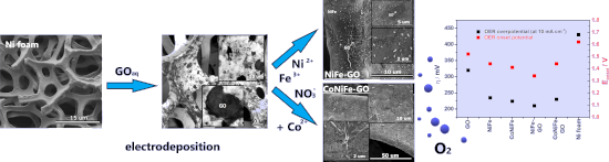
- state in which the local sp2 bonding is influenced mainly by oxygen functionalization [32][33]. The position of the peak and the intensity of the spectra differ for NiFe-GO and CoNiFe-GO, indicating different electronic structures and interactions around Ni, Fe, Co, and GO. Figure 3e presents the XRD
- , Eonset: 1.34 V). Thus, the presence of both nickel in the oxidation state 3+ and the LDH structure results in a more efficient OER reaction. XAS analysis indicated the change in the electronic structure of the catalysts after the addition of GO (Figure 3). The analysis showed that the electronic
- structure around nickel and iron was changed, which may be associated with interactions between NiFe or CoNiFe and GO (carbon domains). Something similar was observed in the case of the addition of N-doped nanocarbon to NiFe [16]. To summarize, the disturbed morphology and the change in the electronic


Plasmonic nanotechnology for photothermal applications – an evaluation
Beilstein J. Nanotechnol. 2023, 14, 380–419, doi:10.3762/bjnano.14.33

- electronic, translation, vibration, and rotational transitions. The interaction time period of electromagnetic radiation with electrons is around 10−14 to 10−15 s. SPR falls within the regime of electronic transitions and, generally, electronic transitions can be interband as well as intraband transitions
- curvature [35]. Finally, changes to the material composition, such as through doping or vacancy processing, can affect the LSPR because of changes in the free electron density, the electron effective mass, and the electronic band structure in general [36][37]. An understanding of the changes in absorbance
- ultimate conversion of electron scattering into heat. The energy distribution of hot carriers (which decides the relaxation times) depends on the electronic band structure [78], particle size, density of states, and the geometry of nanoparticles [79]. Figure 12 shows the vast differences in the population


Bismuth-based nanostructured photocatalysts for the remediation of antibiotics and organic dyes
Beilstein J. Nanotechnol. 2023, 14, 291–321, doi:10.3762/bjnano.14.26

- plasmonic and photocatalytic properties. The typical and most recently applied bismuth-based nanostructure photocatalysts are depicted in Figure 2. Structural, optoelectronic, and magnetic properties Bismuth's peculiar optical, electronic, and more recently discovered photocatalytic and plasmonic properties
- important for electronic transport and semimetal-to-semiconductor transition, as well as its highly anisotropic Fermi surface (with an electron and hole Fermi energies of 27.2 and 10.8 meV, respectively), which results in an extremely low carrier density of around 3 × 1017 cm−3 [78] and very little overlap
- visible in Bi nanowires with a diameter of around 1–3 nm, but as the diameter increased, they became less visible because of the intense quantum confinement effect. In addition to the electronic properties of Bi, its outstanding optical properties have a big impact on how effective it is as a


Structural, optical, and bioimaging characterization of carbon quantum dots solvothermally synthesized from o-phenylenediamine
Beilstein J. Nanotechnol. 2023, 14, 165–174, doi:10.3762/bjnano.14.17

- (QDs) of nanometer scale, the CQD edges influence the electronic structure of the conjugated sp2 domains [35][36]. Figure 2 shows FTIR, UV–vis and PL spectra of CQDs/PU composite samples. It is obvious from Figure 2a that there are some additional peaks in the CQDs/PU FTIR spectrum compared to that of


Batch preparation of nanofibers containing nanoparticles by an electrospinning device with multiple air inlets
Beilstein J. Nanotechnol. 2023, 14, 141–150, doi:10.3762/bjnano.14.15

- purification. Preparation of spinning solution Firstly, 4.5 g PAN and 44 g DMF solution were weighed separately by an electronic balance (XJ120A, Shanghai Precisa Co., LTD), mixed and placed on an unheated magnetic stirrer (HJ-6A, Gongyi Yuhua Instrument Co., LTD.) for stirring for 24 h. Then 1.5 g ZnO
- using an electronic balance (XJ120A, Precisa LTD.). The nanofiber morphology was investigated by a scanning electron microscopy (SEM, Hitachi S4800, Hitachi LTD.), and Image J software (National Institute of Mental Health) was used to characterize the fiber diameter distribution by random selection of


Characterisation of a micrometer-scale active plasmonic element by means of complementary computational and experimental methods
Beilstein J. Nanotechnol. 2023, 14, 110–122, doi:10.3762/bjnano.14.12

- underneath and its ability to interact with electronic circuits [22]. The performance of the active element can be characterised in terms of modulation localisation and depth. Localisation addresses how confined the active control is at the nanoscale, while modulation depth is an indicator of how well the


