Search results
Search for "sensor" in Full Text gives 445 result(s) in Beilstein Journal of Nanotechnology. Showing first 200.
Hydrophilicity and carbon chain length effects on the gas sensing properties of chemoresistive, self-assembled monolayer carbon nanotube sensors
Beilstein J. Nanotechnol. 2019, 10, 565–577, doi:10.3762/bjnano.10.58

- attributed to the interaction, via strong hydrogen bonding, of the polar molecules tested to the polar surface of hydrophilic thiols. The approach discussed here could be extended further by combining hydrophilic and hydrophobic thiol SAMs in Au-MWCNT sensor arrays as a helpful strategy for tuning sensor
- gas sensitive nanomaterial to higher temperatures [3] or to irradiate the sensor employing ultraviolet (UV) light, in order to promote surface cleaning. Despite these efforts, sometimes CNTs present irreversible resistance changes due to the chemisorption of gas molecules. In addition, other problems
- such as lack of selectivity, environmental variations (e.g., changes in humidity level) affecting sensor response, or the difficulty to detect gases characterized by low adsorption energies are often encountered [11]. In order to enhance their selectivity and/or their sensitivity, CNTs have been


Wearable, stable, highly sensitive hydrogel–graphene strain sensors
Beilstein J. Nanotechnol. 2019, 10, 475–480, doi:10.3762/bjnano.10.47

- 21500, P. R. China Research institute of Xi'an Jiaotong University, Hangzhou, Zhejiang, 311215, P. R. China 10.3762/bjnano.10.47 Abstract A stable and highly sensitive graphene/hydrogel strain sensor is designed by introducing glycerol as a co-solvent in the formation of a hydrogel substrate and then
- casting a graphene solution onto the hydrogel in a simple, two-step method. This hydrogel-based strain sensor can effectively retain water in the polymer network due to the formation of strong hydrogen bonding between glycerol and water. The addition of glycerol not only enhances the stability of the
- sensor to be used in both stretching and bending modes. As a demonstration, the as-prepared strain sensor was applied to sense the movement of finger knuckles. Given the outstanding performance of this wearable sensor, together with the proposed scalable fabrication method, this stable and sensitive


Temperature-dependent Raman spectroscopy and sensor applications of PtSe2 nanosheets synthesized by wet chemistry
Beilstein J. Nanotechnol. 2019, 10, 467–474, doi:10.3762/bjnano.10.46

- well with the reported 2D transition metal dichalcogenides. A PtSe2 nanosheet-based sensor device was tested for its applicability as a humidity sensor and photodetector. The humidity sensor based on PtSe2 nanosheets showed an excellent recovery time of ≈5 s, indicating the great potential of PtSe2 for
- future sensor devices. Keywords: nanosheets; PtSe2; Raman spectroscopy; sensor; thermal effect; Introduction Graphene, the most well-studied example of the two-dimensional (2D) aromatic compounds, is the building block of all forms of carbon allotropes [1]. In recent years, it has been widely studied
- onto a Si substrate and heated at 100 °C on a hot plate. After complete evaporation, the substrate was annealed in a chemical vapour deposition system at 500 °C in argon gas atmosphere for 5 h. Supporting Information File 1, Figure S1 shows the schematic of the PtSe2 nanosheet synthesis steps. Sensor


Ultraviolet patterns of flowers revealed in polymer replica – caused by surface architecture
Beilstein J. Nanotechnol. 2019, 10, 459–466, doi:10.3762/bjnano.10.45

- (Camag, Muttenz, Switzerland) illumination at 366 nm. An extension of the sensor detection spectrum of the D 300s camera from 340 nm to 1100 nm was implemented by Optik Makario (Mönchengladbach, Germany) and allowed images in the UV-spectrum to be captured. An analog Nikon FM2 was used to take pictures


Sub-wavelength waveguide properties of 1D and surface-functionalized SnO2 nanostructures of various morphologies
Beilstein J. Nanotechnol. 2019, 10, 379–388, doi:10.3762/bjnano.10.37

- commercial application as a gas sensor, transparent conducting electrodes, and catalyst [13][14][15]. SnO2 NSs have been used in several other areas such as sub-wavelength waveguide sensors [4], microelectronics [6], Li-ion batteries [16], and lubricants [17]. Oxygen vacancy related defects in SnO2


Transport signatures of an Andreev molecule in a quantum dot–superconductor–quantum dot setup
Beilstein J. Nanotechnol. 2019, 10, 363–378, doi:10.3762/bjnano.10.36

- the price of decreasing the currents, too. Charge sensing [76][77] is another method to map out the boundaries of the phase diagram, as we illustrate in the right column of Figure 2. A charge sensor is usually engineered to be mostly sensitive to the average electron occupation of one of the quantum
- charge sensor is an additional device element. Similar methods, yielding information related to average electron occupation, are based on reflectometry with electromagnetic radiofrequency signals [78][79] or microwave resonators [80][81]; those are not discussed further in this work. The ground-state
- tunnel-coupled to the QD–SC–QD system. Transport Calculation As pointed out earlier, a charge-sensing measurement is demanding, since the addition of the charge sensor complicates device fabrication. However, the ground-state phase diagrams discussed above can also be explored experimentally by


Intuitive human interface to a scanning tunnelling microscope: observation of parity oscillations for a single atomic chain
Beilstein J. Nanotechnol. 2019, 10, 337–348, doi:10.3762/bjnano.10.33

- structural evolution of the junction during the manipulation operation and alter the trajectory at will. Figure 1 shows the scheme of communication between operator and STM using the MD simulator. The 3D motion tracking sensor sends the same x,y,z- signals to both the STM and the simulator simultaneously and
- the operator, and depends on the speed with which the 3D motion control sensor is moved. In the scale of the operator this is approximately 5 cm/sec, which corresponds to 1 Å/sec on the atomic scale. We perform a classical MD simulation here in which we ignore the electronic effects (which in fact


Nitrous oxide as an effective AFM tip functionalization: a comparative study
Beilstein J. Nanotechnol. 2019, 10, 315–321, doi:10.3762/bjnano.10.30

- with exposures of 0.5–1.7 L. AFM measurements were performed with a qPlus sensor (resonance frequency ca. 30 kHz; k ≈ 1800 N/m), using an oscillation amplitude of 50 pm. Prior to functionalization, the Pt tip was repeatedly indented into the Au(111) substrate several nanometers deep for sharpening and


Relation between thickness, crystallite size and magnetoresistance of nanostructured La1−xSrxMnyO3±δ films for magnetic field sensors
Beilstein J. Nanotechnol. 2019, 10, 256–261, doi:10.3762/bjnano.10.24

- films consisting of columnar nanograins have already been successfully applied for the sensing of high pulsed magnetic fields (B-scalar sensor) [13][14]. Despite this development, the scalar (independent of field orientation) CMR effect under a low magnetic field is still a challenging goal towards


Magnetic-field sensor with self-reference characteristic based on a magnetic fluid and independent plasmonic dual resonances
Beilstein J. Nanotechnol. 2019, 10, 247–255, doi:10.3762/bjnano.10.23
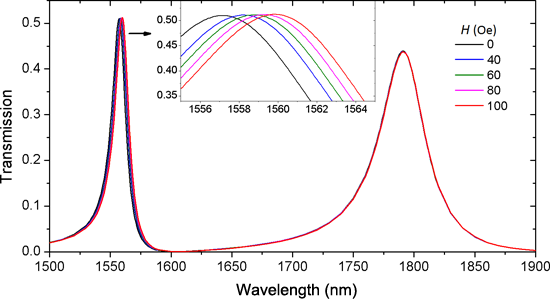
- , Tianjin 300222, China 10.3762/bjnano.10.23 Abstract A magnetic-field sensor with self-reference characteristic based on metal–dielectric–metal (MDM) plasmonic waveguides and a magnetic fluid (MF) is proposed and theoretically investigated. Independent dual resonances are supported by the coupled
- resonances on the external field, a magnetic-field sensor with self-reference characteristic is achieved. The magnetic-field nanosensor shows an excellent performance with a high sensitivity of 27 pm/Oe, i.e., 270 pm/mT. The proposed sensor takes advantage of the refractive-index tunability of the MF and the
- compactness of the MDM waveguide structure. This research may open new opportunities to design nanoscale magnetic sensors with good performance. Keywords: dual resonance; magnetic fluid; magnetic sensor; plasmonic waveguide; self-reference; surface plasmon polaritons; Introduction Sensors that can detect


Wet chemistry route for the decoration of carbon nanotubes with iron oxide nanoparticles for gas sensing
Beilstein J. Nanotechnol. 2019, 10, 105–118, doi:10.3762/bjnano.10.10

- with iron oxide nanoparticles substantially ameliorated the response towards nitrogen dioxide. Keywords: benzene detection; doping; gas sensor; metal nanoparticle decoration; multiwalled carbon nanotubes; NO2 detection; room temperature gas sensing; surface modification; Introduction Carbon nanotubes
- ) well below air quality guidelines [24][25], which indicates the importance of fabricating such a gas sensor to be used in different applications. In this paper, we report on a wet chemistry route that was successfully employed to chemically modify CNTs by decorating them with iron oxide nanoparticles
- study of the gas sensing properties of the different hybrid nanomaterials was conducted in an effort to determine the optimal functionalization parameters to maximize sensor response. The selectivity of the resulting layer for potential interfering gases such as CO and benzene has also been investigated


Graphene–graphite hybrid epoxy composites with controllable workability for thermal management
Beilstein J. Nanotechnol. 2019, 10, 95–104, doi:10.3762/bjnano.10.9

- method requires a transiently heated plane sensor, which consists of an electrically conducting pattern in the shape of a double spiral. This spiral is sandwiched between two thin sheets of an insulating material (kapton). When performing a TD measurement, the plane Hot Disk sensor is fitted within the
- two composite samples. While heating up, the sensor measures the temperature increase inside the sample over time. The time-dependent change in temperature is used to calculate the TD and thermal conductivity of the measured material. The measurements were conducted in air at 25 °C [67]. Electron


Pull-off and friction forces of micropatterned elastomers on soft substrates: the effects of pattern length scale and stiffness
Beilstein J. Nanotechnol. 2019, 10, 79–94, doi:10.3762/bjnano.10.8

- samples without a terminal layer. For these two conditions, one of the five measurements could not be completed because the sensor reached its maximum capacity. Because of the small sample size, we refrained from presenting boxplots with median and interquartile range, and present only raw data instead
- friction stress on glass for samples of PDMS-580 with various geometries and feature sizes. Sub-microscale samples without terminal layer seem to generate higher friction than the remainder of the samples, but we refrain from drawing any conclusions, as for 6 out of the 35 measurements the sensor reached


Bidirectional biomimetic flow sensing with antiparallel and curved artificial hair sensors
Beilstein J. Nanotechnol. 2019, 10, 32–46, doi:10.3762/bjnano.10.4

- stimuli. Inspired by the neuromasts found in the lateral line of fish, we present a novel flow sensor design based on two curved cantilevers with bending orientation antiparallel to each other. Antiparallel cantilever pairs were designed, fabricated and compared to a single cantilever based hair sensor in
- μV/(m s−1) for a higher air flow velocity range (between ±20–32 m s−1). The antiparallel cantilever design improves directional sensitivity and provides a sinusoidal response to flow angle. In forward flow, the single sensor reaches its saturation limitation, flattening at 67% of the ideal sinusoidal
- curve which is earlier than the antiparallel cantilevers at 75%. The antiparallel artificial hair sensor better compensates for temperature changes than the single sensor. Conclusion: This work demonstrated the successive improvement of the bidirectional sensitivity, that is, improved temperature


Zn/F-doped tin oxide nanoparticles synthesized by laser pyrolysis: structural and optical properties
Beilstein J. Nanotechnol. 2019, 10, 9–21, doi:10.3762/bjnano.10.2

- ], photocatalysts for rhodamine 6G dye degradation in aqueous solution [27] and were proposed as a thermal UV sensor for high-radiation environments [4]. Moreover, the ZTO materials were also employed as volatile organic compound (VOC) (such as methanol, ethanol or acetone vapors) sensors [28], as an anode for Li


A new bioinspired method for pressure and flow sensing based on the underwater air-retaining surface of the backswimmer Notonecta
Beilstein J. Nanotechnol. 2018, 9, 3039–3047, doi:10.3762/bjnano.9.282

- . Keywords: mechanoreceptor; Notonecta sensor; pressure sensor; Salvinia effect; superhydrophobic surfaces; Introduction The surfaces of animals and plants are interfaces between the organisms and the environment. Since animals and plants inhabit many different environments, it is not surprising that over
- mechanosensitive setae not only for drag reduction, but also for the detection of prey or predators. With one exception [16], the involvement of air layers in a sensory function has never been demonstrated. A possible principle for a sensor that uses an air layer for the detection of pressure changes is shown in
- a technical air-retaining surface and an optical sensor (for details see Experimental section). With this setup (Figure 8), which represents a biomimetic proof of principle, we were able to record the verbal conversation of two persons standing in front of the experimental tank. This was the final


Electrostatic force microscopy for the accurate characterization of interphases in nanocomposites
Beilstein J. Nanotechnol. 2018, 9, 2999–3012, doi:10.3762/bjnano.9.279

- , while exciting the probe at its first eigenmode f0 [58]. During the first scan, sample topography was extracted and collected on a first image using the tapping mode. For the second scan, the sensor was lifted by a known distance from the surface, the so-called “lift” distance, and controlled to follow


Size limits of magnetic-domain engineering in continuous in-plane exchange-bias prototype films
Beilstein J. Nanotechnol. 2018, 9, 2968–2979, doi:10.3762/bjnano.9.276

- sensor applications [3][4][5], for stray field design [6][7] and particle transport in lab-on-chip systems [8][9][10][11], or in spintronics and magnonics [12][13][14]. Currently available techniques for domain patterning are either based on focused ion beams (FIB) [15][16][17], ion implantation [18][19
- ][20][21], laser annealing [22][23][24], thermally assisted scanning probe lithography [25], or a combination of spatially broad laser- or ion-beams and shadow masks [26][27][28][29][30]. Especially in magnonic [14] and sensor applications [4] in-plane magnetic domain patterns play a key role and are


![[Graphic 63]](/bjnano/content/inline/2190-4286-9-276-i63.svg?max-width=637&scale=1.18182) .
. ![[Graphic 64]](/bjnano/content/inline/2190-4286-9-276-i64.svg?max-width=637&scale=1.18182) is the angle between the domain wall (DW) normal vector
is the angle between the domain wall (DW) normal vector ![[Graphic 65]](/bjnano/content/inline/2190-4286-9-276-i65.svg?max-width=637&scale=1.18182) and the local unidirectio...
and the local unidirectio...
Investigation of CVD graphene as-grown on Cu foil using simultaneous scanning tunneling/atomic force microscopy
Beilstein J. Nanotechnol. 2018, 9, 2953–2959, doi:10.3762/bjnano.9.274

- are attached to the end of the sensor. The use of metallic tips is particularly crucial in simultaneous measurement of tunnel current and force. Force values are calculated from oscillation amplitude data using the equation above for carbon and hollow sites. This was done for both constant-current (CC


Time-resolved universal temperature measurements using NaYF4:Er3+,Yb3+ upconverting nanoparticles in an electrospray jet
Beilstein J. Nanotechnol. 2018, 9, 2916–2924, doi:10.3762/bjnano.9.270

- ability to be used as a universal temperature sensor. Herein, we introduce a universal calibration protocol for NaYF4:Er3+,Yb3+ upconverting nanoparticles that is robust to environmental changes and gives a precise temperature measurement. We used this new procedure to calculate the temperature profile
- temperature is determined by measuring the ratio of two green photoluminescence bands where the relative intensities are temperature-dependent and related by a Boltzmann factor. We used this thermal sensor to probe the thermal properties at a solid–water interface and found that a nanoscale object optically
- sensor using Er2O3 nanoparticles [37]. (A) An image showing an electrospray jet of 0.8 pM upconverting solution (yellow lines) from a glass pipette (green lines). The red circle represents the tip of a Taylor cone. (B) Emission spectra of UCNPs at different regions as marked in panel (A) with respective


Charged particle single nanometre manufacturing
Beilstein J. Nanotechnol. 2018, 9, 2855–2882, doi:10.3762/bjnano.9.266

- microscopy or force–distance measurements, without the use of additional optical read-out. In Figure 15 an active cantilever is shown, together with a close-up view of the sharp tip at the end of the cantilever. This active cantilever is equipped with a thermomechanical actuator and a piezo-resistive sensor
- . Thereby, a DC voltage generates a static deflection whereas an AC voltage can drive an oscillation of the cantilever. The deflection is determined by the heat generated resistively and up to 30 µm peak-to-peak values of the actuation amplitude can be achieved [149]. The deflection sensor comprises four
- piezo-resistors configured in an integrated Wheatstone bridge to reduce the influence of noise and temperature [150][151]. A simulation model was developed to optimize the size, length and placement of the heater and the deflection sensor [148][152]. Other actuation and sensing principles can be used as


Nanostructure-induced performance degradation of WO3·nH2O for energy conversion and storage devices
Beilstein J. Nanotechnol. 2018, 9, 2845–2854, doi:10.3762/bjnano.9.265

- applications [24][33][34]. Oriented WO3·H2O sheets were hydrothermally grown in mixed acids at 80 °C for 17 h, followed by sintering at 500 °C in order to obtain crystalline WO3 for the photoelectrochemical water oxidation [35]. A 2D WO3 nanosheet sensor fabricated by high-temperature anodization of tungsten


Graphene-enhanced metal oxide gas sensors at room temperature: a review
Beilstein J. Nanotechnol. 2018, 9, 2832–2844, doi:10.3762/bjnano.9.264

- . The improved experimental schemes are raised and the critical research directions of graphene/metal-oxide sensors in the future are proposed. Keywords: gas sensor; graphene; metal oxide; nitrogen dioxide (NO2); room temperature; Review Introduction Since the discovery by Novoselov and Geim [1
- , thus converting it to a semiconductor. Choi et al. [11] prepared GO room-temperature gas sensors by a modified Hummers method. The group found that the sensitivity and repeatability of the sensor depended on the amount of oxygen functional groups on the surface of GO. Moreover, hydroxy groups were the
- ]. The oxygen functional groups that locate on the surface of rGO lead to an electron transfer from rGO to oxygen functional groups, and holes become the main charge carriers, indicating that rGO acts as a p-type semiconductor [14][15][16]. Zhang et al. [17] prepared rGO room-temperature gas sensor with


Accurate control of the covalent functionalization of single-walled carbon nanotubes for the electro-enzymatically controlled oxidation of biomolecules
Beilstein J. Nanotechnol. 2018, 9, 2750–2762, doi:10.3762/bjnano.9.257

- arising from the non-covalent interaction between CNTs and the electron mediator is that the latter may diffuse inside the analyzed medium, resulting in a progressive decrease of the sensor efficiency. A good alternative is therefore to covalently graft an electron mediator onto the CNT sidewalls. While


Au–Si plasmonic platforms: synthesis, structure and FDTD simulations
Beilstein J. Nanotechnol. 2018, 9, 2599–2608, doi:10.3762/bjnano.9.241

- on the sample. The time envelope of the pulse was set to be rectangular. It provided the single wavelength of 395 nm (which is the off-resonant transition for Si) for exactly 10 fs. The sensor was placed in the zx-plane, 10 nm above the Si substrate. The second simulation, by using FDTD and discrete
- . The sensor was placed in the zx-plane, between the light source and the nanoparticle layer, to allow for recording both incident and reflected fluxes. In both cases the pulse propagated along the y-axis, perpendicular to the sample surface, and was of a collimated phase front with a power of 1 W; the


