


Search results
Search for "AFM tips" in Full Text gives 45 result(s) in Beilstein Journal of Nanotechnology.
He+ FIBID-fabricated 3D AFM tip architectures: an exploratory study of hollow pillars, helices, and spirals
Beilstein J. Nanotechnol. 2026, 17, 863–871, doi:10.3762/bjnano.17.62
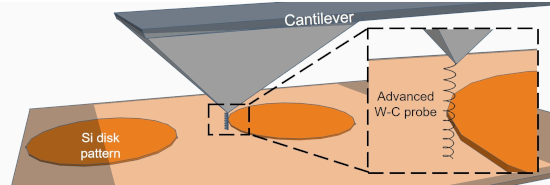
- , Germany 10.3762/bjnano.17.62 Abstract Atomic force microscopy (AFM) relies strongly on tip geometry and mechanical integrity for stable and reproducible surface measurements. Here, we present an exploratory study of tungsten–carbon (W–C) AFM tips with complex three-dimensional (3D) architectures
- required. Keywords: 3D-printed tips; AFM tips; beam induced nanomanufacturing; focused ion beam induced deposition (FIBID); helium ion microscope; nanohelix; nanopillar; nanospiral; scanning tip microscopy; surface topography; tungsten carbide; Introduction The atomic force microscope (AFM) is a
- developed, including both in situ and ex situ approaches [22][24][26][27][28][29][30][31]. While these methods can significantly improve material purity and functional properties, their application to AFM tips requires particular consideration. In tip-based applications, post-deposition treatments may alter


Advancing nanolithography: a comprehensive review of materials for local anodic oxidation with AFM
Beilstein J. Nanotechnol. 2026, 17, 275–291, doi:10.3762/bjnano.17.19
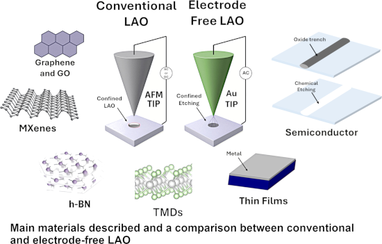
- minimum feature size. Carbon nanotube (CNT)-functionalized AFM tips have been explored for LAO [49][60][61] because their high aspect ratio and good conductivity can, in principle, enable sharper and more controlled oxidation. However, their practical performance is limited by mechanical fragility and


Ultrathin water layers on mannosylated gold nanoparticles
Beilstein J. Nanotechnol. 2025, 16, 2183–2198, doi:10.3762/bjnano.16.151
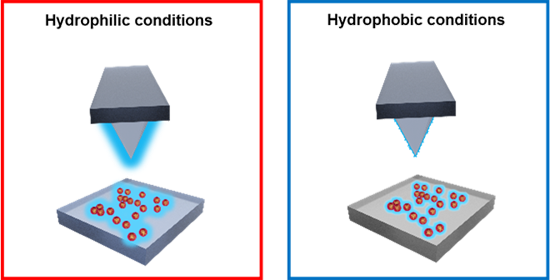
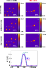
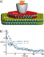
- repeated the experiments under hydrophobic conditions: We employed OTS silicon surfaces and hydrophobic carbon AFM tips. From this, we exclude that the observed phenomena is specific for the type of surface [36] or based on mechanical contact between tip and surface [22][23][37]. The ∆z value under ambient
- assembly by AFM and SEM complement the results discussed above. The use of hydrophilic and hydrophobic surfaces and also AFM tips allows one to distinguish ubiquitous water layers, present on all surfaces, from specific water adsorption on the AuNPs. For the APDMES surface at neutral pH, we expect
- hydrophobic AFM tips, helped us to exclude the role of water adsorbed on the surfaces. We found a 100% thickness increase of the 1.5 nm thick dimannoside ligand shell (i.e., 1.5 nm of water), corresponding to about four layers of water. The water can be absorbed in a layer or absorbed among the various



Design, fabrication, and characterization of kinetic-inductive force sensors for scanning probe applications
Beilstein J. Nanotechnol. 2024, 15, 242–255, doi:10.3762/bjnano.15.23
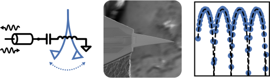
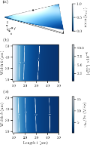
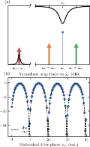
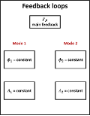
- highly desirable. Furthermore, we would like the integrated sensor package, that is, transducer and detector, to be easily exchangeable, as AFM tips are frequently damaged when scanning over unknown surface features. Dynamic AFM is typically operated in two alternative modes of scanning feedback, namely



Quantitative wear evaluation of tips based on sharp structures
Beilstein J. Nanotechnol. 2024, 15, 230–241, doi:10.3762/bjnano.15.22
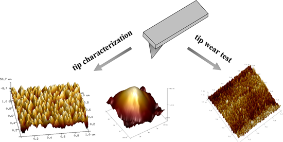
- structures is proposed. This research explored the wear of AFM tips during tapping mode and examined the effects of scanning parameters on estimated tip diameter and surface roughness. The experiment results show that the non-destructive method for measuring tip morphology is highly repeatable. Additionally
- in assessing the topography of AFM tips and delves into the effects of scanning parameters on tip wear. A method employing TipCheck samples has been introduced to determine the shape and structure of AFM tips accurately. Based on its distinct features, the tip morphology can be non-destructively
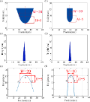
- scan images of the TipCheck sample. (a) 2D topography image and (b) 3D topography image. Extraction of scan line feature points. SEM images of AFM tips. (a) Image of tip and cantilever beam and (b) image of the tip; the dotted frame is a partially enlarged view of the tip. Reconstructed probe model. (a




Determination of the radii of coated and uncoated silicon AFM sharp tips using a height calibration standard grating and a nonlinear regression function
Beilstein J. Nanotechnol. 2023, 14, 1200–1207, doi:10.3762/bjnano.14.99
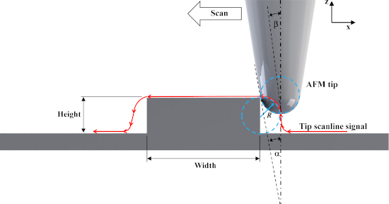
- addition, those studies are limited to the use of uncoated AFM tips with reflectively coated cantilevers. Here, we present the actual measurement of the radius of coated and uncoated AFM tips using the contact scan mode with sub-nanonewton normal load on a height calibration standard grating. The round
- . AFM Tips and Calibration Standard Grating Three types of AFM sharp tips were used, namely a Pt-coated tip (HQ:NSC18/Pt, nominal radius < 30 nm for electrical, force modulation AFM; Figure 1a), a Cr/Au-coated tip (HQ:NSC16/Cr-Au, nominal radius < 35 nm for tapping mode AFM; Figure 1b), and an uncoated
- of SiO2 with height = 20 nm, grate distance = 2 µm, and pitch distance = 5 µm, on top of a silicon substrate, which allows for more space for the AFM tips to sweep along the height grate geometry. The corner edge radius of the grating height is not provided in the specification [15]. However, recent


Exploring internal structures and properties of terpolymer fibers via real-space characterizations
Beilstein J. Nanotechnol. 2023, 14, 1004–1017, doi:10.3762/bjnano.14.83
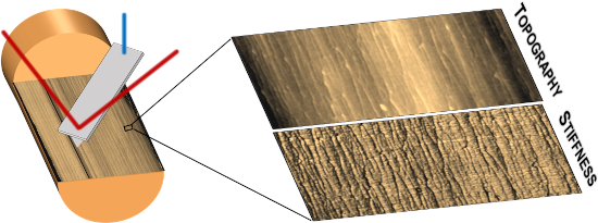
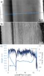
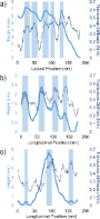
- . Transverse elastic modulus quantifications We present these last results as relative stiffness variations because multiple AFM tips needed to be used to survey these multiple subdomains. Monitoring tip wear is cumbersome when targeting a broad survey of different regions of multiple fibers, so the results
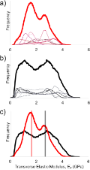
- , that is, using AFM tips with different shapes and sizes, or worn tips, will yield different stiffness values. Thus, when presenting transverse stiffness values, we focus on the relative variations within different maps. Maps of transverse elastic modulus (ET), quantified in [GPa], directly quantify
- subdomains (typically 500 nm × 500 nm, ca. 1 nm/pixel) to reduce the likelihood of tip wear. In addition, subdomains were initially mapped out with “sacrificial” AFM tips, and ET distributions were only then obtained from scans with fresh, well-characterized AFM tips. In quantitative scans, the shape of each






Studies of probe tip materials by atomic force microscopy: a review
Beilstein J. Nanotechnol. 2022, 13, 1256–1267, doi:10.3762/bjnano.13.104
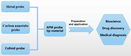
- and poorly controlled. Cheng et al. [11] introduced a method to selectively prepare individual carbon nanotubes on AFM tips by controlling the trigger threshold to regulate the growth solution on the tip. The obtained carbon nanotube probes are of suitable length and do not require a subsequent
- shows that AFM tips sharpened by extracting individual metal nanoclusters can significantly reduce vdW interactions between the tip and the sample and improve spatial resolution. This type of nano-tip is exceptionally robust and can detect different samples. It is expected that tip functionalization
Temperature and chemical effects on the interfacial energy between a Ga–In–Sn eutectic liquid alloy and nanoscopic asperities
Beilstein J. Nanotechnol. 2022, 13, 817–827, doi:10.3762/bjnano.13.72
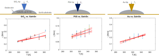
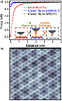
- atomic force microscopy (AFM) tips of different chemistries as a function of the temperature (T = 21–90 °C) by AFM force spectroscopy using an XE100 AFM equipped with a heating stage (manufactured by Park Instruments, Republic of Korea). We recorded force–distance curves with PtSi-coated Si cantilevers
- and calculate the corresponding work of adhesion Wad as suggested in [19] for solid interfaces. The authors measured the adhesion between atomically smooth quasicrystalline surfaces of TiN-coated AFM tips in ultrahigh vacuum by analyzing the pull-off force during atomic force spectroscopy measurements
- surface of the eutectic Ga–In–Sn melt with three AFM tips of different chemistries, namely SiOx, PtSi, and Au. Figure 2 also indicates the surface roughness Rq value for each topography image. We recorded the presented topography images in contact mode by setting and controlling the normal force to Fn = 2



The role of convolutional neural networks in scanning probe microscopy: a review
Beilstein J. Nanotechnol. 2021, 12, 878–901, doi:10.3762/bjnano.12.66







Application of contact-resonance AFM methods to polymer samples
Beilstein J. Nanotechnol. 2020, 11, 1714–1727, doi:10.3762/bjnano.11.154
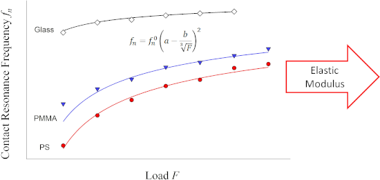
- with a Cypher AFM (Asylum Research, Oxford Instruments, Santa Barbara, USA). Two kinds of silicon AFM tips have been used: PPP-FMAuD (kc ≅ 3 N/m) from Nanosensors (NanoWorld, Neuchatel, Switzerland) and AC240 (kc = 0.775 N/m) from Asylum Research. Additional measurements have been done with a silica


Protruding hydrogen atoms as markers for the molecular orientation of a metallocene
Beilstein J. Nanotechnol. 2020, 11, 1432–1438, doi:10.3762/bjnano.11.127
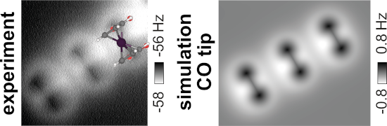
- experiments (5 and 77 K) with qPlus sensors as well as at room temperature using silicon cantilevers [22]. Although the NC-AFM tips were not functionalised, i.e., not specifically terminated with atoms or molecules for imaging, we find a very good agreement between the experimental data and probe particle
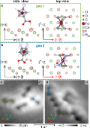


![[Graphic 10]](/bjnano/content/inline/2190-4286-11-127-i10.svg?max-width=637&scale=1.18182) row of FDCA molecules in geo 2. (a–c) Constant-height frequency-shi...
row of FDCA molecules in geo 2. (a–c) Constant-height frequency-shi...
Atomic defect classification of the H–Si(100) surface through multi-mode scanning probe microscopy
Beilstein J. Nanotechnol. 2020, 11, 1346–1360, doi:10.3762/bjnano.11.119
- -functionalized AFM tips to image the molecular structure of pentacene [28]. Other functionalisations of AFM tips have been explored including Cu–O tips [29][30] and Xe tips [31][32]. The use of H2 [33][34] and D2 [35] provided the first successful demonstration of the enhanced imaging contrast by scanning
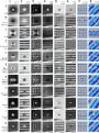
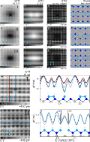
- using a field ion microscope (FIM) [90]. AFM tips used the third-generation Giessibl tuning forks with a FIB mounted tungsten tip (f0 ≈ 28 kHz, Q-factor ≈ 16k–22k) [91]. The tip was cleaned and sharpened in vacuum using a FIM [90]. In situ tip conditioning was done by executing controlled contact on a
- hydrogen-desorbed patch of silicon [43][92]. Bright contrast, H-functionalised AFM tips were routinely formed with controlled contact on H-terminated portions of the surface, while bare silicon AFM tips were formed using only desorbed patches (although not all controlled contacts on a desorbed patch



Revealing the local crystallinity of single silicon core–shell nanowires using tip-enhanced Raman spectroscopy
Beilstein J. Nanotechnol. 2020, 11, 1147–1156, doi:10.3762/bjnano.11.99
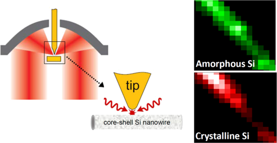
- antenna. This nanoantenna is typically made by chemical etching of a thin Ag or Au wire or by evaporating a Ag or Au thin film on AFM tips. The tip works like an optical antenna when it is brought as close as a few nanometers to the sample surface and when it is illuminated with a tightly focused laser


Quantitative determination of the interaction potential between two surfaces using frequency-modulated atomic force microscopy
Beilstein J. Nanotechnol. 2020, 11, 729–739, doi:10.3762/bjnano.11.60
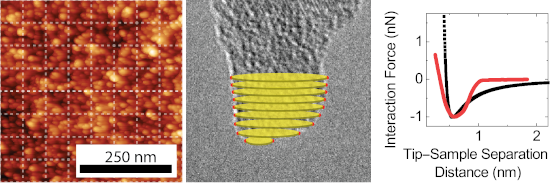
- 0.6 ± 0.2 nm, where the error represents the standard deviation of the mean values determined. Qualitatively comparable observations were made with the other AFM tips tested in these series of measurements. There is limited literature pertaining to the Wadh and z0 values for a silicon/SiOx–diamond


Charged particle single nanometre manufacturing
Beilstein J. Nanotechnol. 2018, 9, 2855–2882, doi:10.3762/bjnano.9.266
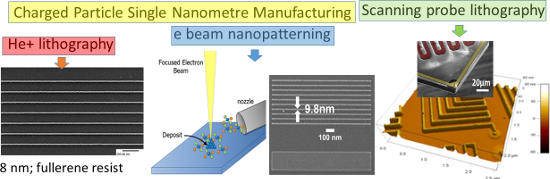
- sample preparation. In addition, there are no restrictions on the substrate to be patterned, accommodating everything from flat wafers to AFM tips. Extensive reviews of EBID and EBIE can be found in [47][48][49][50]. Due to the versatility of FEBIP, it has been used for several different applications


Low cost tips for tip-enhanced Raman spectroscopy fabricated by two-step electrochemical etching of 125 µm diameter gold wires
Beilstein J. Nanotechnol. 2018, 9, 2718–2729, doi:10.3762/bjnano.9.254
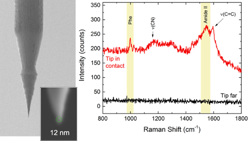
- tip [29][30]. TERS tips are nowadays produced by the chemical/electrochemical etching of metal wires [31][32][33][34][35], metal coatings of AFM tips [36][37][38], electroless deposition, [39] galvanic displacement [40] or by advanced nanostructuration techniques such as electron beam induced
- deposition (EBID) and focused ion beam (FIB) milling [41][42][43] (see [30][44] for reviews). Fabrication methods capable of guaranteeing high reproducibility, cost-effectiveness and scalability to industrial production are, however, still not available at present. Metal vapor deposition on AFM tips is
- nanocube monomers [53] predict a 100-fold smaller light emission with respect to the nanocube-on-surface configuration, and the origin of the signal is attributed to photoluminescence rather than to ERS. Sanders et al. [57], working on Au-coated spherical AFM tips, have shown a remarkable correlation


Nanoscale characterization of the temporary adhesive of the sea urchin Paracentrotus lividus
Beilstein J. Nanotechnol. 2018, 9, 2277–2286, doi:10.3762/bjnano.9.212
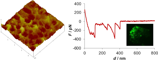
- artificial seawater (ASW)) exhibited a mean pull-off force of 0.41 ± 0.20 nN [2]. Later on, adhesive footprints were probed in a moist environment with ASW using different AFM tips (Si3N4 and functionalized with CH3 terminal groups) and the obtained force–extension curves exhibited the characteristic


Recent highlights in nanoscale and mesoscale friction
Beilstein J. Nanotechnol. 2018, 9, 1995–2014, doi:10.3762/bjnano.9.190
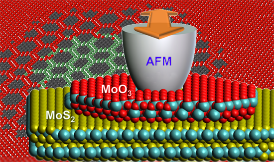
- the latter term should be considered to be more accurate [42]. The experimental analysis of structural lubricity has long since been difficult, because well-defined junctions between conventional AFM tips and substrates cannot readily be found for single-asperity contacts. Instead, the detailed
- structure and composition of AFM tips is often ill-defined and therefore obstructs any systematic analysis of problems where accurate interface structures are required [43]. As a consequence, a growing number of studies is now focusing on friction of sliding nano-objects, where well-defined interfaces are


Friction force microscopy of tribochemistry and interfacial ageing for the SiOx/Si/Au system
Beilstein J. Nanotechnol. 2018, 9, 1647–1658, doi:10.3762/bjnano.9.157
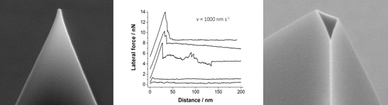
- sequence was performed first with tips with intact passivating layer and then repeated with activated tips. Electron microscopy (SEM, TEM) Contamination and modification of the AFM tips were examined by scanning electron microscopy (10 kV acceleration voltage) using secondary-electron and backscattered
- passivating Si(100), as we did not find any wear debris on the tips or on the surfaces. Wear rates of sharp AFM tips after sliding distances of up to 1 μm against diamond have been calculated earlier [24]. The wear volumes and sliding distances were much smaller than in our experiments but the wear rates of
- lateral forces. The AFM tips were worn flat with an angle imposed by the geometry of the AFM. The flat was smooth and no wear debris was found. Therefore an adhesive wear process where single atoms were removed through formation and breaking of chemical bonds is a most likely microscopic scenario [24][25




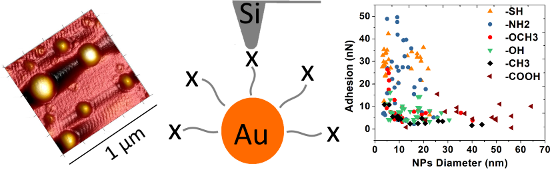
Tuning adhesion forces between functionalized gold colloidal nanoparticles and silicon AFM tips: role of ligands and capillary forces
Beilstein J. Nanotechnol. 2018, 9, 660–670, doi:10.3762/bjnano.9.61


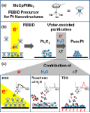
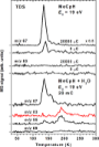
Electron-driven and thermal chemistry during water-assisted purification of platinum nanomaterials generated by electron beam induced deposition
Beilstein J. Nanotechnol. 2018, 9, 77–90, doi:10.3762/bjnano.9.10
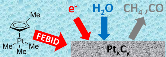
- ]. Applications of this technology range from repair of masks for photolithography [2] and the fabrication of AFM tips [1] to novel photonic [3][4] or plasmonically active [5] devices and sensor concepts [6]. Also, nanoscale structures grown by FEBID may possess promising magnetic properties [7][8]. However



A robust AFM-based method for locally measuring the elasticity of samples
Beilstein J. Nanotechnol. 2018, 9, 1–10, doi:10.3762/bjnano.9.1
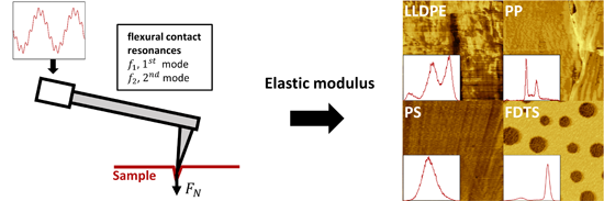
- soft FDTS-coating of the tip is sensed (see also Figure 8). The effect of collecting Teflon-like molecules with AFM tips has been known for a long time. It has been successfully used for the topographic imaging of the Si(111) surface with atomic resolution. Howald et al. [27] studied the Si(111) 7 × 7


The rational design of a Au(I) precursor for focused electron beam induced deposition
Beilstein J. Nanotechnol. 2017, 8, 2753–2765, doi:10.3762/bjnano.8.274
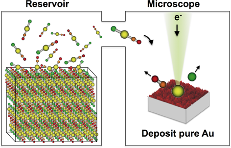
- be etched [16]. As it is damage-free, it is used for repairing the masks for ultraviolet and extreme ultraviolet lithography [17][18], which is a major industry. FEBIP also enables the prototyping of 3D structures, such as AFM tips [19] and photonically active components [20], and the direct


Exploring wear at the nanoscale with circular mode atomic force microscopy
Beilstein J. Nanotechnol. 2017, 8, 2662–2668, doi:10.3762/bjnano.8.266
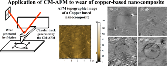
- humidity of 30%. The AFM tips were either a unique DLC coating tip with a rectangular cantilever (from NT-MDT) or a unique silicon nitride (Si3N4) probe with a triangular cantilever. Both nominal tip radius values were 100 nm and 70 nm for the DLC and Si3N4 probes, respectively, and the cantilever





