Search results
Search for "UPS" in Full Text gives 65 result(s) in Beilstein Journal of Nanotechnology.
Recent progress in enhancing built-in electric fields of perovskite solar cells via junction engineering
Beilstein J. Nanotechnol. 2026, 17, 602–621, doi:10.3762/bjnano.17.42

- to p-type, and thus induced a vertical p–n homojunction in the lower bulk region of the film. This band restructuring significantly amplified and extended the BEF, thereby facilitating directional charge separation and transport. Ultraviolet photoelectron spectroscopy (UPS) revealed an increase in
- constructing an n–p homojunction. Accordingly, UPS and Kelvin probe force microscopy (KPFM) measurements showed that the surface work function increased by about 0.5 eV and the potential difference increased by about 0.26 V. Mott–Schottky analysis further revealed an increase in Vbi of roughly 0.1 V
- compositional gradient with Sn enrichment at the bottom and Pb enrichment at the top. TOF-SIMS depth profiling and UPS measurements confirmed that this gradient introduced approximately 0.32 eV of band bending within the bulk, which generated a quasi-BEF even without external bias, raising the Vbi to 0.96 V


Functional surface engineering for cultural heritage protection: the role of superhydrophobic and superoleophobic coatings – a comprehensive review
Beilstein J. Nanotechnol. 2026, 17, 63–96, doi:10.3762/bjnano.17.6

- principles. Ethyl lactate acts as the organic solvent, PHB as the gelator, and DFO as a chelating agent for Fe(III), all functioning effectively at a mildly acidic pH (~4.8). The authors prepared several mock-ups of mild steel by chemically inducing corrosion and coating with Paraloid® B72, replicating real
- conservation challenges. Application of the PHB–EL–DFO gel on these mock-ups demonstrated its ability to safely and efficiently remove both corrosion products and polymer coatings, even when coatings penetrated the corrosion layer. The gel was prepared at 110 °C and cooled to form a malleable, easy-to-use


Insights into the electronic and atomic structures of cerium oxide-based ultrathin films and nanostructures using high-brilliance light sources
Beilstein J. Nanotechnol. 2025, 16, 860–871, doi:10.3762/bjnano.16.65

- between spin–orbit split lines [24]. In contrast, Ce 3d spectra exhibit five partially overlapped spin–orbit split components originating from different final states, which complicate the analysis [40]. Synchrotron radiation-based photoemission has proven to be significantly more versatile than XPS/UPS


Direct electron beam writing of silver using a β-diketonate precursor: first insights
Beilstein J. Nanotechnol. 2024, 15, 1117–1124, doi:10.3762/bjnano.15.90

- evaporation temperatures for 3D printing. (a) Scanning electron micrograph showing the upper right quadrant of a square deposit with the different halo regions and their close-ups and (b) the corresponding simulated range of SE + BSE. The white dashed line in (a) indicates the position of the cross-sectional
- cut for the TEM sample preparation. (c) Transmission electron micrograph of the deposit cross-section with close-ups (d–f). Scanning electron micrographs of a spot deposit with 60 min continuous spot irradiation (a) with the corresponding close-ups of the halo regions. (b) High-resolution SEM image 6


Ultrasensitive and ultrastretchable metal crack strain sensor based on helical polydimethylsiloxane
Beilstein J. Nanotechnol. 2024, 15, 270–278, doi:10.3762/bjnano.15.25

- sensor. Insets: close-ups of the selected areas. (e) Hysteresis curve of the helical strain sensor at 280% strain. (f) Frequency tests at an applied strain of 0 to 200%. (g) Durability test for 1000 stretch–release cycles under 150% strain. (h) Comparison of maximum working range and GF of the helical


CdSe/ZnS quantum dots as a booster in the active layer of distributed ternary organic photovoltaics
Beilstein J. Nanotechnol. 2024, 15, 144–156, doi:10.3762/bjnano.15.14

- relations of refractive indices and extinction coefficient were investigated. The morphologies of the thin films were studied with atomic force microscopy. The chemical boundaries of the ternary layers were determined by Raman spectroscopy. Based on UPS studies, the energy diagram of the potential devices
- monocrystalline silicon. A WITec Alpha 300 M+ spectrometer with a 488 nm laser, 600 groove grating, and a 100× ZEISS objective was used for Raman measurements. The samples were deposited on a glass substrate. Ultraviolet photoelectron spectroscopy (UPS) was conducted in an ultrahigh-vacuum chamber with a base
- pressure of approximately 8 × 10⁻¹⁰ mbar, using the XPS/UPS/ARPES PREVAC setup. The analysis chamber was equipped with a PREVAC Ea15 hemispherical analyzer and a PREVAC EA15 40B source (UV power U = 0.56 kV, PUV = 55 W, He I). The beam energy scale was calibrated at the Fermi level of 16.87 eV. The samples


Self-assembly of C60 on a ZnTPP/Fe(001)–p(1 × 1)O substrate: observation of a quasi-freestanding C60 monolayer
Beilstein J. Nanotechnol. 2022, 13, 857–864, doi:10.3762/bjnano.13.76

- keeping the sample grounded and applying a continuous or sinusoidal bias voltage to the tip. We followed the convention to indicate as positive the bias for which electrons tunnel from filled states of the tip to empty states of the sample. The ultraviolet photoelectron spectroscopy (UPS) data have been
- acquired at normal emission with a 150 mm hemispherical electron analyzer from SPECS GmbH. The probing depth of UPS is a few angstroms [49]. A He lamp has been employed as a source of non-monochromatized unpolarized UV photons. The He-I line, with a photon energy of 21.2 eV, has been used to excite the
- sample. The full width at half maximum (FWHM) energy resolution of the UPS experiment is 0.05 eV. Results and Discussion Figure 1a and Figure 1b report the structural characterization of the ZnTPP/Fe(001)–p(1 × 1)O sample in the reciprocal and in direct space, respectively. The low-energy electron


Investigation of a memory effect in a Au/(Ti–Cu)Ox-gradient thin film/TiAlV structure
Beilstein J. Nanotechnol. 2022, 13, 265–273, doi:10.3762/bjnano.13.21

- 284.8 eV. Ultraviolet photoelectron spectroscopy (UPS) was performed using a non-monochromatic He I line (21.22 eV) excitation source with a step size of 0.025 eV. A bias voltage of −5 V was applied to the thin film sample during UPS measurements to obtain a clear secondary electron cutoff. The binding
- energies of the spectra were referred to the Fermi level (EF) determined from a cleaned reference Au sample. Measurement results were analyzed with the aid of CasaXPS software. In the case of XPS and UPS measurements, the results were averaged over a certain surface area, that is, the beam diameter was
- related to lattice oxygen (for TiO2 and CuO), hydroxy groups (OH−) and adsorbed water molecules (H2Oads). The UPS spectrum of the (Ti0.48Cu0.52)Ox thin film is shown in Figure 7. The position of the valence band maximum (VBM) was determined from the extrapolation of the line fit to the leading edge of the


Bio-imaging with the helium-ion microscope: A review
Beilstein J. Nanotechnol. 2021, 12, 1–23, doi:10.3762/bjnano.12.1


Free and partially encapsulated manganese ferrite nanoparticles in multiwall carbon nanotubes
Beilstein J. Nanotechnol. 2020, 11, 1891–1904, doi:10.3762/bjnano.11.170

- values was estimated to be equal to ±0.1 eV. Due to the charging effect of the oxides, electron flooding was carried out for charge compensation. A helium lamp with 21.2 eV (He I) excitation energy was used for ultraviolet photoemission spectroscopy (UPS, Omicron Nanotechnology). A −5 V sample bias was
- are the first UPS measurements carried out for this system. Figure 1e provides the structure of the valence band of free MnFe2O4 nanoparticles. Experimental results indicate that the density of states (DOS) at the Fermi level, EF (i.e., at a zero binding energy in the UPS spectrum) is consistent with
- graphite and it is explained by the destabilization of π electrons due to the curvature of the graphene sheets [35]. As observed from Figure 1e and Figure 6, there are large spectral differences between free MnFe2O4, MnFe2O4/MWCNTs, and pristine MWCNTs. Considering that the probing depth of UPS is only at


Application of contact-resonance AFM methods to polymer samples
Beilstein J. Nanotechnol. 2020, 11, 1714–1727, doi:10.3762/bjnano.11.154

- DART measurement leads to a depression of the whole scanned area, eventually accompanied by the formation of pile-ups. For example, measurements on a 120 nm thick PS film with a static force higher than ca. 250 nN leave depressions that are visible even with an optical microscope, and the depth of
- of a depression, eventually accompanied by pile-ups at the sides of the scan surface. In this case, the mechanical properties are altered because of the changes in thickness and, more important, because of compression. (3) Even when the load is not high enough to modify the whole scan surface through


The influence of an interfacial hBN layer on the fluorescence of an organic molecule
Beilstein J. Nanotechnol. 2020, 11, 1663–1684, doi:10.3762/bjnano.11.149

- PTCDA and hBN/Cu(111) is weak and physisorptive [32] as opposed to the chemisorptive bond between PTCDA and Cu(111) [33]. Ultraviolet photoelectron spectroscopy (UPS) experiments showed that on the Cu(111) surface the chemical bonding leads to a filling of the LUMO [33]. In contrast, on hBN/Cu(111), the
- PTCDA from Cu(111). For PTCDA on Ag(111) and Au(111) [39], it has been shown that FL can only be observed from the second and third molecular layer onward. The excitation of the first layers is completely quenched by the metal substrates as described above. In UPS experiments, a partial filling of the
- LUMO of PTCDA was found on Ag(111), but not on Au(111) [33]. Thus, the quenching on Ag(111) is directly understood by the static charge transfer seen in UPS. The quenching on Au(111), not as evident from UPS, demonstrates the sensitivity of FL spectroscopy to an overlap of wave functions of excited


Impact of fluorination on interface energetics and growth of pentacene on Ag(111)
Beilstein J. Nanotechnol. 2020, 11, 1361–1370, doi:10.3762/bjnano.11.120

- ) on Ag(111) via X-ray standing waves (XSW), low-energy electron diffraction (LEED) as well as ultraviolet and X-ray photoelectron spectroscopy (UPS and XPS). XSW revealed that the adsorption distances of F4PEN in (sub)monolayers on Ag(111) were 3.00 Å for carbon atoms and 3.05 Å for fluorine atoms
- ][30][31][32][33][34][35]. PEN and PFP have almost identical optical gaps in thin films (1.85 eV and 1.75 eV, respectively) [36][37], and the experimental gas phase IEs (measured by UPS) are 6.59 eV [38] and 7.50 eV [39], respectively. This trend of the IEs is also found for thin films comprised of PEN
- alignment was investigated by UPS. Furthermore, we compared the adsorption behavior of F4PEN on Ag(111) with that of PEN and PFP on the same substrate to understand the influence of fluorine substitution on the interfacial electronic structure of prototypical pentacene derivatives at organic–metal


Hybridization vs decoupling: influence of an h-BN interlayer on the physical properties of a lander-type molecule on Ni(111)
Beilstein J. Nanotechnol. 2020, 11, 1168–1177, doi:10.3762/bjnano.11.101

- The ultraviolet photoelectron spectroscopy (UPS) measurements of the DBP films on Ni(111) and h-BN/Ni(111) are depicted in Figure 4. We use the notation proposed by Kirchhuebel et al. to assign spectroscopic features to the underlying molecular orbitals, taking into consideration the probing process
- [37]. Within this notation, each feature is ascribed to the involved molecular orbital with the probing process being characterized by the initial state as subscript and the final state as a superscript. For example, a single-photon photoionization (UPS measurement) describes a transition from the
- identification of the underlying orbitals very difficult. The UPS features of DBP on h-BN/Ni(111), on the other hand, are much sharper and shifted to higher binding energies. The reduction of the line width can be explained by an increase of the structural order, which was already discussed in the last section


Label-free highly sensitive probe detection with novel hierarchical SERS substrates fabricated by nanoindentation and chemical reaction methods
Beilstein J. Nanotechnol. 2019, 10, 2483–2496, doi:10.3762/bjnano.10.239

- form a structure similar to fish scales with fx = 5 μm and fy = 1 μm. Additionally, the inside of the cavities and the surface of the sample are smooth. However, the surface of the sample, the inside of the cavities, and pile-ups of material are roughened when using HCl and AgNO3 solutions. Ag
- nanoparticles are generated on different positions including inside the cavities, in the pile-ups of material, and the surface of the sample as shown in Figure 1b–e. Figure 1b shows SEM images of arrayed triangular cavities etched by AgNO3 with fx = 2 μm and fy = 1 μm. More complex structures can be generated
- via the adjacent cavities that are overlapped and squeezed using the normal force control method with a decrease in feed (fy). The nanoparticles are generated inside of the cavities and the pile-ups of the cavities using the AgNO3 solution. The SEM images of arrayed pyramidal cavities etched by AgNO3


Kelvin probe force microscopy work function characterization of transition metal oxide crystals under ongoing reduction and oxidation
Beilstein J. Nanotechnol. 2019, 10, 1596–1607, doi:10.3762/bjnano.10.155

- applications are nowadays based on oxide heterostructures, not only is macroscopic information of the work function needed (which may be provided by averaging techniques such as ultraviolet photoelectron spectroscopy (UPS)) but also spatial resolution on the nanoscale. Driven by its remarkable lateral and
- ) eV, which is almost 1 eV lower than previous X-ray photoemission electron microscopy (XPEEM) and UPS studies (4.13 and 4.2 eV) for untreated oxide [32][33]. As stated before, KPFM investigations reveal certain variations in the work function value of TiO nanostructures. To illustrate this properly a
- pristine TiO crystal. To date, the only values for the TiO WF come from polycrystalline samples (films, nanoparticles) and from the laterally averaging method of UPS, thus this cannot be reasonably compared with our findings. The WF value obtained for the reduced SrTiO3(100) surface of 3.12(18) eV follows


Kelvin probe force microscopy of the nanoscale electrical surface potential barrier of metal/semiconductor interfaces in ambient atmosphere
Beilstein J. Nanotechnol. 2019, 10, 1401–1411, doi:10.3762/bjnano.10.138

- photoelectron spectroscopy (UPS) in UHV at the macroscale. The existence of the Schottky barrier was demonstrated at +120 meV for the Mo layer and −80 meV for the Au layer reflecting the formation of MoSe2 and Au/Bi2Se3 alloy, respectively. The results of both methods (KPFM and UPS) were in good agreement. We
- voltage of 20 kV (which results in a penetration depth of the electrons of 1 µm into Bi2Se3) for a period of maximally 360 s. The work function (WF) was determined by utraviolet photoelectron spectroscopy (UPS) using a helium gas discharge source with He I radiation (hν = 21.22 eV). All UPS measurements
- functions were measured by surface-sensitive ultraviolet photoelectron spectroscopy (UPS) (Figure 8) employing He I irradiation (hν = 21.22 eV) with an information depth up to 3 nm. The work function was determined from UPS spectra as an intersection between the background and the linear extrapolation of


Imaging the surface potential at the steps on the rutile TiO2(110) surface by Kelvin probe force microscopy
Beilstein J. Nanotechnol. 2019, 10, 1228–1236, doi:10.3762/bjnano.10.122

- ]. Concerning the charge properties of steps on TiO2, it has been measured with using ultraviolet photoelectron spectroscopy (UPS) that surfaces with a high step density have a lower work function than surfaces with a low step density [28]. The local change in the surface potential at steps on TiO2 has been

![[Graphic 16]](/bjnano/content/inline/2190-4286-10-122-i16.svg?max-width=637&scale=1.18182) and
and ![[Graphic 17]](/bjnano/content/inline/2190-4286-10-122-i17.svg?max-width=637&scale=1.18182) .
.


![[Graphic 38]](/bjnano/content/inline/2190-4286-10-122-i38.svg?max-width=637&scale=1.18182) and
and ![[Graphic 39]](/bjnano/content/inline/2190-4286-10-122-i39.svg?max-width=637&scale=1.18182) steps. (a) Topographic image...
steps. (a) Topographic image...


![[Graphic 72]](/bjnano/content/inline/2190-4286-10-122-i72.svg?max-width=637&scale=1.18182) , b)
, b) ![[Graphic 73]](/bjnano/content/inline/2190-4286-10-122-i73.svg?max-width=637&scale=1.18182) , c) reduced
, c) reduced ![[Graphic 74]](/bjnano/content/inline/2190-4286-10-122-i74.svg?max-width=637&scale=1.18182) , and d)
, and d) ![[Graphic 75]](/bjnano/content/inline/2190-4286-10-122-i75.svg?max-width=637&scale=1.18182) steps. B...
steps. B...
Charged particle single nanometre manufacturing
Beilstein J. Nanotechnol. 2018, 9, 2855–2882, doi:10.3762/bjnano.9.266

- undesirable effects such as dopant spreading associated with local temperature rise. 3.1.1 Experimental set-ups forFE-eSPL. A pattern is written by moving the scanning probe along a pre-defined path using a piezo-scanner [144]. FE-eSPL systems are typically operated in a constant-current mode [120][126], in


Intrinsic ultrasmall nanoscale silicon turns n-/p-type with SiO2/Si3N4-coating
Beilstein J. Nanotechnol. 2018, 9, 2255–2264, doi:10.3762/bjnano.9.210

- Moore’s law to reach the Si-crystallization limit of ca. 1.5 nm [15]. In our present work, we prove by hybrid-density functional theory (h-DFT) simulations and synchrotron-based long-term ultraviolet photoelectron spectroscopy (UPS) that usn-Si indeed can have a massive ΔE of their electronic density of
- electron microscopy (TEM) and the measurement of the highest occupied DOS over energy for Si-NWell samples embedded in SiO2 or Si3N4 by synchrotron-based long-term UPS. With this experimental confirmation of our h-DFT results, we present the concept of undoped Si-NWire field-effect transistors (FETs). We
- of information on h-DFT accuracy as compared to experiment, details of UPS measurements and NEGF are contained in Supporting Information File 1. Experimental h-DFT material calculations Hybrid-DFT calculations were carried out in real space with a molecular orbital basis set (MO-BS) and both Hartree


Spin-coated planar Sb2S3 hybrid solar cells approaching 5% efficiency
Beilstein J. Nanotechnol. 2018, 9, 2114–2124, doi:10.3762/bjnano.9.200

- Sb2S3 cells by the polymer is to a large extent parasitic [27]. The applied polymers differ in band gap as can be seen from the measured absorption spectra in Figure 4c and the position of the highest occupied molecular orbital (HOMO). The HOMO of Sb2S3 obtained from ultraviolet photon spectroscopy (UPS
- ) measurements is reported to lie between 5.3 and 5.5 eV [30][51][63] with one report claiming 5.9 eV [32]. Reported HOMO values of the polymers are 4.9–5.1 eV for P3HT [64][65] and 5.3–5.4 eV for KP115 [61][66] and are obtained from cyclic voltammetry measurements, which yields lower lying HOMO levels than UPS


Fatigue crack growth characteristics of Fe and Ni under cyclic loading using a quasi-continuum method
Beilstein J. Nanotechnol. 2018, 9, 1000–1014, doi:10.3762/bjnano.9.93

- . Zhang et al. have examined the effect of the phase boundary on the fatigue crack propagation in an α/β-iron biphasic system under cyclic tensile loading [13]. They found that the nucleation of new cracks typically appears at the phase boundary because of dislocation pile-ups. However, most of these


Cyclodextrin inhibits zinc corrosion by destabilizing point defect formation in the oxide layer
Beilstein J. Nanotechnol. 2018, 9, 936–944, doi:10.3762/bjnano.9.86
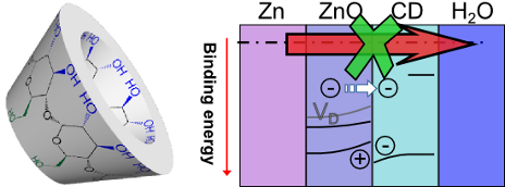
- , with Raman spectra of the interface proving the adsorption of the intact β-CD. Angular dependent X-ray photoelectron spectroscopy (ADXPS) and ultraviolet photoelectron spectroscopy (UPS) were used to extract a band-like diagram of the β-CD/ZnO interface, showing a large energy level shift at the
- containing electrolyte, samples were analysed by angle-dependent X-ray photoelectron spectroscopy (ADXPS) combined with ultraviolet photoelectron spectroscopy (UPS). Results and Discussion Electrochemical measurements of the corrosion potential Ecorr displayed in Figure 1a show a cathodic shift by several
- shift for all energy regions [35], as opposed to what is observed. Since the XPS was not sensitive for the region of the highest occupied molecular orbital (HOMO) of β-CD, this region was analyzed by UPS. Figure 3f presents the magnification of the low-energy onset of the UP spectra, which allows for


Nematic topological defects positionally controlled by geometry and external fields
Beilstein J. Nanotechnol. 2018, 9, 109–118, doi:10.3762/bjnano.9.13

- mimic geometric set-ups that could be realized experimentally using, for instance, the atomic force microscope (AFM) scribing method [17]. In a typical experimental set up one confines a nematic LC within a thin plane-parallel cell, where at least one (“master”) surface imposes anchoring conditions


![[Graphic 25]](/bjnano/content/inline/2190-4286-9-13-i36.svg?max-width=637&scale=1.18182) with the largest positive eigenvalue, corresponding to the 2D biaxi...
with the largest positive eigenvalue, corresponding to the 2D biaxi...


Transition from silicene monolayer to thin Si films on Ag(111): comparison between experimental data and Monte Carlo simulation
Beilstein J. Nanotechnol. 2018, 9, 48–56, doi:10.3762/bjnano.9.7

- form and the film becomes more and more inhomogeneous, resulting in a larger fraction of the surface uncovered by the thick Si islands. Experimental Experiments were performed in two UHV set-ups with 10−10 mbar base pressure. The Ag(111) sample was cleaned by series of cycles of Ar ion sputtering at


