Search results
Search for "charge transport" in Full Text gives 123 result(s) in Beilstein Journal of Nanotechnology.
Flexible freestanding MoS2-based composite paper for energy conversion and storage
Beilstein J. Nanotechnol. 2019, 10, 1488–1496, doi:10.3762/bjnano.10.147

- ][34]. However, MoS2 possesses only a low intrinsic conductivity, which hinders the charge transport [35]. Using MoS2 together with conducting support materials, such as multiwalled carbon nanotubes (MWCNTs) has already been demonstrated to improve the catalytic properties [35]. Herein, we report on


Electroluminescence and current–voltage measurements of single-(In,Ga)N/GaN-nanowire light-emitting diodes in a nanowire ensemble
Beilstein J. Nanotechnol. 2019, 10, 1177–1187, doi:10.3762/bjnano.10.117

- a slight decrease. However, the decisive difference is that for the ensemble measurement the fraction of NWs participating in charge transport and emitting EL can only be roughly estimated, essentially because the NWs in the dense ensemble cannot be optically resolved [12]. Furthermore, from the


An efficient electrode material for high performance solid-state hybrid supercapacitors based on a Cu/CuO/porous carbon nanofiber/TiO2 hybrid composite
Beilstein J. Nanotechnol. 2019, 10, 781–793, doi:10.3762/bjnano.10.78

- channels for faster ionic charge transport to enhance the capacitance performance of the Cu/CuO/PCNF/TiO2 composite material. To study the internal resistance of the electrode and the electrode/electrolyte resistance of supercapacitors based on polymer gel electrolyte, electrochemical impedance
- diffusion and adsorption onto the electrode surface. (ii) A high number mesopores allows effective access to the electrolyte to the electrode surface due to easier ionic charge transport through the number of channels, thus improving the electrochemical properties of composite electrode material. (iii) The


Hydrophilicity and carbon chain length effects on the gas sensing properties of chemoresistive, self-assembled monolayer carbon nanotube sensors
Beilstein J. Nanotechnol. 2019, 10, 565–577, doi:10.3762/bjnano.10.58

- approach, carbon nanotubes act as support and charge transport transducing elements while the recognition function is performed by grafted molecules. Two examples of this have consisted of obtaining thiol-functionalized carbon nanotube buckypapers [27] or self-assembled monolayers (SAMs) of thiol molecules
- S1, Supporting Information File 1). While thiol molecules behave as a chemoselective material responsible for the recognition of gas species, carbon nanotubes act as efficient charge transport networks, enabling the implementation of a chemoresistive transduction. Different thiols were attached to
- principle, behave as a chemoselective material responsible for the recognition of gas species. In contrast, carbon nanotubes should not play a major role as receptors for target gas molecules, but instead act as efficient charge transport networks, enabling the efficient implementation of chemoresistive


Advanced scanning probe lithography using anatase-to-rutile transition to create localized TiO2 nanorods
Beilstein J. Nanotechnol. 2019, 10, 412–418, doi:10.3762/bjnano.10.40

- and might charge the film locally. The charges are likely trapped in defect states generated by the scratching process. Furthermore, the native silicon oxide layer prevents a quick charge transport into the conductive boron-doped silicon substrate. A charged film might attract the precursor more


A Ni(OH)2 nanopetals network for high-performance supercapacitors synthesized by immersing Ni nanofoam in water
Beilstein J. Nanotechnol. 2019, 10, 281–293, doi:10.3762/bjnano.10.27

- peaks, which is related to the poor conductivity (larger ohmic resistance) of Ni(OH)2 nanopetals [21][43]. Larger ohmic resistance leads to slow kinetics of charge transport and interfacial charge transfer of the material. Thus, the electrode reaction rate slows down, resulting in a reduced


Interaction of Te and Se interlayers with Ag or Au nanofilms in sandwich structures
Beilstein J. Nanotechnol. 2019, 10, 238–246, doi:10.3762/bjnano.10.22

- ], enhanced abrasive properties of metal films [9] as well as effects like charge transport anisotropy [10] and giant magneto-optical Kerr response [11]. We have recently shown that depositing silver with an ultrathin germanium interlayer alters the density profile of the silver film [12]. Among the most


Amorphous NixCoyP-supported TiO2 nanotube arrays as an efficient hydrogen evolution reaction electrocatalyst in acidic solution
Beilstein J. Nanotechnol. 2019, 10, 62–70, doi:10.3762/bjnano.10.6

- -frequency area correspond to the impedance of charge transport inside the electrode [15][42][43][44]. In Figure 8a, the Nyquist curves are shown as two arcs with different radius in the high and low frequency, suggesting that the catalytic reaction was limited by the charge transfer step. The arc radii of


Lead-free hybrid perovskites for photovoltaics
Beilstein J. Nanotechnol. 2018, 9, 2209–2235, doi:10.3762/bjnano.9.207

- open-circuit voltage of up to 1.19 V and fill factor (FF) of almost 90% when introduced into inverted solar cells with PEDOT:PSS and PCBM charge transport layers [101]. Despite the high Voc and FF values, the cells showed quite a low efficiency of ≈0.3% indicating huge recombinational losses and
- (Figure 13a). As this modification has a relatively low charge transport efficiency, various approaches are developed to forward the HP formation to other modifications, including the above-discussed introduction of Cl− ions as well as the replacement of bulky cations with smaller ones, for example, with
- nanocrystals (NCs) [16][24][28][29][30][43][50][53][54][55][56]. Recently, broad recognition was gained by 1D and 2D layered hybrid perovskite materials with strong anisotropy of electron properties. Such materials are currently treated as very promising light harvesters with highly tunable optical and charge


Electrospun one-dimensional nanostructures: a new horizon for gas sensing materials
Beilstein J. Nanotechnol. 2018, 9, 2128–2170, doi:10.3762/bjnano.9.202


Spin-coated planar Sb2S3 hybrid solar cells approaching 5% efficiency
Beilstein J. Nanotechnol. 2018, 9, 2114–2124, doi:10.3762/bjnano.9.200

- [32] or liquid [6] sulfur sources might reduce the density of electronic defects in Sb2S3 for certain deposition methods that leave sulfur deficient films [29][72]. Another aim in terms of fabrication is to exploit the anisotropic nature of Sb2S3 by aligning the 1D ribbons with the direction of charge
- transport between the contacts. A beneficial effect was demonstrated for the structurally identical Sb2Se3 [9]. A proper substrate choice or embedding a seed layer might be the key to directed growth in Sb2S3. Experimental Chemicals: All chemicals were purchased from Sigma-Aldrich except for KP115 which was


Numerical analysis of single-point spectroscopy curves used in photo-carrier dynamics measurements by Kelvin probe force microscopy under frequency-modulated excitation
Beilstein J. Nanotechnol. 2018, 9, 1834–1843, doi:10.3762/bjnano.9.175

- account the built-up time of the SPV, which is the time needed for the surface photovoltage to appear in the first place. This time is associated with the exciton generation, charge dissociation and charge transport along the material so that a photo-generated surface potential can be detected using KPFM


Robust topological phase in proximitized core–shell nanowires coupled to multiple superconductors
Beilstein J. Nanotechnol. 2018, 9, 1512–1526, doi:10.3762/bjnano.9.142

- produced in a charge transport measurement by tunneling electrons between the semiconductor wire and external electrodes attached to its ends [14][15][16][17][18][19][20][21][22][23][24]. These experiments have provided strong indications regarding the presence of Majorana bound states at the end of the


![[Graphic 30]](/bjnano/content/inline/2190-4286-9-142-i36.svg?max-width=637&scale=1.18182) ) = 0 and
) = 0 and ![[Graphic 31]](/bjnano/content/inline/2190-4286-9-142-i37.svg?max-width=637&scale=1.18182) = 0. The white areas are t...
= 0. The white areas are t...


![[Graphic 40]](/bjnano/content/inline/2190-4286-9-142-i46.svg?max-width=637&scale=1.18182) ) ≠ 0 and
) ≠ 0 and ![[Graphic 41]](/bjnano/content/inline/2190-4286-9-142-i47.svg?max-width=637&scale=1.18182) = 0. The white areas are topol...
= 0. The white areas are topol...

![[Graphic 50]](/bjnano/content/inline/2190-4286-9-142-i56.svg?max-width=637&scale=1.18182) ) ≠ 0 and
) ≠ 0 and ![[Graphic 51]](/bjnano/content/inline/2190-4286-9-142-i57.svg?max-width=637&scale=1.18182) 1 = 0,
1 = 0, ![[Graphic 52]](/bjnano/content/inline/2190-4286-9-142-i58.svg?max-width=637&scale=1.18182) 3 = π/2,
3 = π/2, ![[Graphic 53]](/bjnano/content/inline/2190-4286-9-142-i59.svg?max-width=637&scale=1.18182) 5 = −π/2. T...
5 = −π/2. T...

![[Graphic 65]](/bjnano/content/inline/2190-4286-9-142-i71.svg?max-width=637&scale=1.18182) ) ≠ 0 and
) ≠ 0 and ![[Graphic 66]](/bjnano/content/inline/2190-4286-9-142-i72.svg?max-width=637&scale=1.18182) 1 = π/2,
1 = π/2, ![[Graphic 67]](/bjnano/content/inline/2190-4286-9-142-i73.svg?max-width=637&scale=1.18182) 3 = −π/2,
3 = −π/2, ![[Graphic 68]](/bjnano/content/inline/2190-4286-9-142-i74.svg?max-width=637&scale=1.18182) 5 = π/2, and ...
5 = π/2, and ...


![[Graphic 79]](/bjnano/content/inline/2190-4286-9-142-i85.svg?max-width=637&scale=1.18182) = 3 of a triangular wi...
= 3 of a triangular wi...


Cr(VI) remediation from aqueous environment through modified-TiO2-mediated photocatalytic reduction
Beilstein J. Nanotechnol. 2018, 9, 1448–1470, doi:10.3762/bjnano.9.137

- charge transfer (lower PL peak) of Cu2O-modified TiO2 than the pure TiO2 [96]. The enhanced charge transport efficiency can be found from photoelectrochemical studies using a three electrode system (working electrode, counter electrode and reference electrode). A current intensity–applied voltage (I–V
- (e.g., MFe2O4) results in a smaller arc radius of the Nyquist plot, as shown in Figure 6, and hence, better charge transport is observed [97]. Modification of TiO2 with carbon-based advanced materials Advanced carbon nanomaterials, such as graphene and its derivatives, carbon nanotubes (CNTs) and
- spheres have also been prepared by Chen et al. A coating of an ultrathin TiO2 layer on CdS nanoparticles imparts good light harvesting properties, enhanced adsorption capacity, effective charge transport and longer lifetime of excitons, for which the core–shell spheres exhibited higher efficiency for


Interplay between pairing and correlations in spin-polarized bound states
Beilstein J. Nanotechnol. 2018, 9, 1370–1380, doi:10.3762/bjnano.9.129

- STM tip and the superconducting substrate, inducing a charge transport that, in a subgap regime () originates from the Andreev (particle to hole) scattering mechanism. The polarized Andreev current can be expressed by the Landauer–Büttiker formula where transmittance is defined as and The anomalous


![[Graphic 23]](/bjnano/content/inline/2190-4286-9-129-i39.svg?max-width=637&scale=1.18182) obtained for |J| < Jc in the absence of spin–orbit coupling (le...
obtained for |J| < Jc in the absence of spin–orbit coupling (le...

![[Graphic 26]](/bjnano/content/inline/2190-4286-9-129-i42.svg?max-width=637&scale=1.18182) as a function of the r...
as a function of the r...


Ag2WO4 nanorods decorated with AgI nanoparticles: Novel and efficient visible-light-driven photocatalysts for the degradation of water pollutants
Beilstein J. Nanotechnol. 2018, 9, 1308–1316, doi:10.3762/bjnano.9.123

- impedance spectroscopy (EIS) measurement was applied to study the charge transport and separation [49]. A smaller arc radius commonly signifies a higher charge transport rate. As displayed in Figure 10, the arc radius of 0.3AgI/Ag2WO4 is smaller than that of AgI, suggesting that 0.3AgI/Ag2WO4 holds a higher


Cyclodextrin inhibits zinc corrosion by destabilizing point defect formation in the oxide layer
Beilstein J. Nanotechnol. 2018, 9, 936–944, doi:10.3762/bjnano.9.86
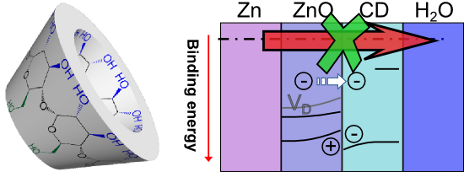
- interface, making the interface behave similarly to an n–p junction. Charge transport is hence only possible from the n-type ZnO to β-CD, which behaves like a p-type layer, effectively blocking the anodic reaction. Most decisively, the energy level shift induced by the changes in the defect chemistry


Perovskite-structured CaTiO3 coupled with g-C3N4 as a heterojunction photocatalyst for organic pollutant degradation
Beilstein J. Nanotechnol. 2018, 9, 671–685, doi:10.3762/bjnano.9.62

- heterojunctions are of great interest in the photocatalysis domain for achieving environmental sustainability [10][11]. These nanocomposites are known for their greater photogenerated electron–hole mobility across the heterojunction interface, which reduces the distance and time of charge transport to impede


Anchoring of a dye precursor on NiO(001) studied by non-contact atomic force microscopy
Beilstein J. Nanotechnol. 2018, 9, 242–249, doi:10.3762/bjnano.9.26

- , Switzerland 10.3762/bjnano.9.26 Abstract The properties of metal oxides, such as charge-transport mechanisms or optoelectronic characteristics, can be modified by functionalization with organic molecules. This kind of organic/inorganic surface is nowadays highly regarded, in particular, for the design of


One-step chemical vapor deposition synthesis and supercapacitor performance of nitrogen-doped porous carbon–carbon nanotube hybrids
Beilstein J. Nanotechnol. 2017, 8, 2669–2679, doi:10.3762/bjnano.8.267

- reduces the resistance at the carbon surface/electrolyte interface and the nanotubes permeating the porous carbon provide fast charge transport in the cell. Keywords: bimetallic catalyst; electrochemical impedance spectroscopy; N-doped carbon; porous carbon–carbon nanotube hybrid; supercapacitor
- . The value is larger when the fraction of porous carbon in the sample is lower (Table S1 in Supporting Information File 1). This fact evidences the role played by the MWCNTs in the enhancement of the charge transport properties of the materials. The fast ion-transfer process in the cells results in


The role of ligands in coinage-metal nanoparticles for electronics
Beilstein J. Nanotechnol. 2017, 8, 2625–2639, doi:10.3762/bjnano.8.263

- substrates to create highly conductive patterns for an electroluminescent device [42]. Yu et al. successfully used silver nanoparticle (Ag NP) inks to prepare grids for polymer solar cells by inkjet or flexographic printing [51]. Charge transport in spaced metal nanoparticle layers is strongly affected by
- inks colloidally stable, but they may prevent electrical contacts in deposited films [32]. Charge transport can be improved after deposition by removing the surface-bound ligands [105], by linking nanoparticles chemically [106], or by ligand exchange in order to manipulate spacing in metal nanoparticle
- well dispersed and had a lower Tp than those with a dense shell, so that conductive films (2 × 10⁵ S/cm) could be formed already at 145 °C. Charge transport also depended on the substituents in ligands, for example, in para-substituted thiophenol ligands on gold nanoparticles. Electron-donating


Inelastic electron tunneling spectroscopy of difurylethene-based photochromic single-molecule junctions
Beilstein J. Nanotechnol. 2017, 8, 2606–2614, doi:10.3762/bjnano.8.261

- theoretical analysis of charge transport through diarylethene-derived single-molecule devices, which are created using the mechanically controlled break-junction technique. Inelastic electron tunneling (IET) spectroscopy measurements performed at 4.2 K are compared with first-principles calculations in the
- properties of several species of photochromic molecules in single-molecule junctions with gold electrodes have been investigated extensively to understand the mechanisms of charge transport and optical switching [11][12][13][14][15][16]. Among the photochromic molecules, diarylethene derivatives are
- , including the energy of the highest occupied molecular orbital (HOMO) and the lowest unoccupied molecular orbital (LUMO) and their coupling to electrodes. This behavior results in a change of the charge transport properties of the corresponding molecular junctions, most prominently of the electrical


Electronic structure, transport, and collective effects in molecular layered systems
Beilstein J. Nanotechnol. 2017, 8, 2094–2105, doi:10.3762/bjnano.8.209

- ; Introduction Implementing molecular spintronics requires the understanding and the ability to modify and control charge-transport characteristics of organic molecules. Thus a solid understanding of the basic effects that govern the transport characteristics in the desired material is required for the


![[Graphic 29]](/bjnano/content/inline/2190-4286-8-209-i41.png?max-width=637&scale=1.18182) between the occupations nA and nB of the two checkerboard sublattices for a) asy...
between the occupations nA and nB of the two checkerboard sublattices for a) asy...

![[Graphic 30]](/bjnano/content/inline/2190-4286-8-209-i42.png?max-width=637&scale=1.18182) per site for a) asymmetric tunneling, Γtop/Γbottom = 0.5, and b) symmetric tunneli...
per site for a) asymmetric tunneling, Γtop/Γbottom = 0.5, and b) symmetric tunneli...
Spin-dependent transport and functional design in organic ferromagnetic devices
Beilstein J. Nanotechnol. 2017, 8, 1919–1931, doi:10.3762/bjnano.8.192

- , namely an inversion of the rectification, may happen. This has been discussed in detail in [59]. Note that the concept of SC rectification reviewed here is based on spin-polarized charge transport. This phenomenon has also been reported in a molecular junction with one ferromagnetic and one nonmagnetic
- -electron and radical spins has so far been treated in a mean-field approximation, which neglects the dynamics of the radical spins. Spin and also charge transport is expected to be affected by the dynamics, which requires a quantum-mechanical description since the radicals typically carry spins S = 1/2


Parylene C as a versatile dielectric material for organic field-effect transistors
Beilstein J. Nanotechnol. 2017, 8, 1532–1545, doi:10.3762/bjnano.8.155

- organic light-emitting diode (OLED) (10−6 g/m2 per day) [23]. Nevertheless, some of the organic semiconductors (mostly electron-transporting materials) require an encapsulation layer, in order to observe charge transport in the transistor architecture [24]. According to our knowledge, there is a limited
- traps but they cannot entirely eliminate surface SiOH groups [39]. When polyethylene was used as a buffer dielectric, unhindered charge transport was observed [40], suggesting that thin polymer layers could play the same role as SAMs do. For this reason, polymers are often used as a part of twin
- hole-type semiconductor. In this case, a more effective charge transport was observed when a Parylene C dielectric film was used instead of the Si/SiO2 combination. An application of parylene insulator also facilitated an evaluation of the influence that the crystalline structure of the semiconductor


