Search results
Search for "convolution" in Full Text gives 87 result(s) in Beilstein Journal of Nanotechnology.
Energy distribution in an ensemble of nanoparticles and its consequences
Beilstein J. Nanotechnol. 2019, 10, 1452–1457, doi:10.3762/bjnano.10.143

- the determination of the particle size distribution is the description of the experimental data by the convolution function. In view of mathematical statistics, the Poisson distribution would be appropriate for particle size distributions stemming from a random process. However, quite often, a normal


Nanoscale spatial mapping of mechanical properties through dynamic atomic force microscopy
Beilstein J. Nanotechnol. 2019, 10, 1332–1347, doi:10.3762/bjnano.10.132

- verify predictions of how the surface behaves under sliding conditions [14]. A previous study of tip convolution on HOPG surfaces [24] illustrated a possible change in the elastic modulus over HOPG steps, but they could not clarify their idea because of the lack of experimental data. Additionally, there
- made about HOPG and graphene step edges to interpret friction and AFM tip-convolution measurements made previously. In this paper, CR AFM is used to clearly identify atomic-scale defects, such as atomic step edges, that show mechanical property variations on surfaces of HOPG. FMM is then used to scan


Influence of dielectric layer thickness and roughness on topographic effects in magnetic force microscopy
Beilstein J. Nanotechnol. 2019, 10, 1056–1064, doi:10.3762/bjnano.10.106

- . The position of the tip dipole is assumed to be at the half radius of the tip [17]. Cross section simulation of MFM phase The first scan of MFM measurements provides a topographic image displaying a convolution of the tip and the nanoparticle [24]. The topographic cross section is simulated by using a
- Gaussian profile at the position of the nanoparticle (black line in Figure 6). The width of the Gaussian profile is much broader than the width of the nanoparticle (assumed to be 12 nm) because of the convolution with the tip with a radius of 84 nm. Both magnetic and electric forces for a single SPION can


![[Graphic 2]](/bjnano/content/inline/2190-4286-10-106-i7.svg?max-width=637&scale=1.18182) ; black line) and measured phase shift for single nanoparticles with 10 ± 2 nm diameter...
; black line) and measured phase shift for single nanoparticles with 10 ± 2 nm diameter...


Self-assembly and wetting properties of gold nanorod–CTAB molecules on HOPG
Beilstein J. Nanotechnol. 2019, 10, 696–705, doi:10.3762/bjnano.10.69

- 4D. This value, however, does not reflect the true height of CTAB. This is due to convolution effects related to the inter-stripe gap (gap width ≈2.5 nm), which is much smaller than the radius of curvature of the AFM tip (≈8 nm). A more accurate estimation of the height of the CTAB stripes can be


Review of time-resolved non-contact electrostatic force microscopy techniques with applications to ionic transport measurements
Beilstein J. Nanotechnol. 2019, 10, 617–633, doi:10.3762/bjnano.10.62

- operating (scanning) parameters (bandwidth of ca. 100 Hz) the PLL response will not affect the extracted values obtained from directly fitting the data. However, as the relaxation time approaches the response time of the PLL, the output signal will become a convolution of the PLL response function and the


Geometrical optimisation of core–shell nanowire arrays for enhanced absorption in thin crystalline silicon heterojunction solar cells
Beilstein J. Nanotechnol. 2019, 10, 322–331, doi:10.3762/bjnano.10.31

- silicon diode with known spectral response was used as reference. The short-current density (Jsc) was determined by a convolution of the measured EQE and the photon flux of the AM1.5 spectrum (). The internal quantum efficiency (IQE) was calculated by dividing the measured EQE by (1 − R), where R is the
- structure were used. Simulation results consists of reflection (R) and absorption (Ai) in each layer (i) of the model, as functions of the wavelength of the incident light. A convolution of the obtained spectral data with the AM1.5 photon flux results in the implied photocurrent density (Jph,i) generated
- explain the boost in absorption observed at (III) in Figure 4. The convolution of Ac−Si with the photon flux of the solar spectrum (Equation 1) allows for the quantification of the optical performance improvement introduced by the presence of nanowires. The implied photocurrent density generated in the


Mechanism of silica–lysozyme composite formation unravelled by in situ fast SAXS
Beilstein J. Nanotechnol. 2019, 10, 182–197, doi:10.3762/bjnano.10.17

- this aggregate as Sint(q), then similar to Hashimoto et al. [43] and Lin et al. [44], we can express the scattering intensity by the generalized Equation 22, in which “” denotes a convolution operation of the functions: where Vagg and represent the volume and the volume fraction of aggregates in the


Enhancement of X-ray emission from nanocolloidal gold suspensions under double-pulse excitation
Beilstein J. Nanotechnol. 2018, 9, 2609–2617, doi:10.3762/bjnano.9.242

- of the water film (a) and the gold nanosphere colloidal solution film (b) at Δt = 6 ns. The laser irradiates the solution film from the right side in these figures. The fit constitutes a multi-Gaussian convolution. The intensity of the pre-pulse is 80 μJ. Under double-pulsed excitation, the spatial


Performance analysis of rigorous coupled-wave analysis and its integration in a coupled modeling approach for optical simulation of complete heterojunction silicon solar cells
Beilstein J. Nanotechnol. 2018, 9, 2315–2329, doi:10.3762/bjnano.9.216

- , especially if simulated at 1 nm wavelength accuracy. The smoother result shown in the figure was achieved by averaging the absorption at 11 wavelengths simulated on 1 nm and presented on 10 nm, as with all other simulations. The convolution of the absorption with a Gaussian function produces similar results


Direct AFM-based nanoscale mapping and tomography of open-circuit voltages for photovoltaics
Beilstein J. Nanotechnol. 2018, 9, 1802–1808, doi:10.3762/bjnano.9.171

- and some sub-granular regions. For any given plane through the specimen it is sometimes difficult to recognize these local properties. This is partially due to convolution with inevitable noise in any SPM-based imaging, but especially results from the stacked and arbitrarily shaped and oriented grains


Magnetic properties of Fe3O4 antidot arrays synthesized by AFIR: atomic layer deposition, focused ion beam and thermal reduction
Beilstein J. Nanotechnol. 2018, 9, 1728–1734, doi:10.3762/bjnano.9.164

- of the magnetic antidots [30]. From this profile, the diameter of the antidots is determined as the full width at half maximum of the hole, and it is measured to be of the order of 70 nm. Moreover, it seems that the holes have a conical structure, but this is due to the convolution with the AFM tip


Closed polymer containers based on phenylboronic esters of resorcinarenes
Beilstein J. Nanotechnol. 2018, 9, 1594–1601, doi:10.3762/bjnano.9.151

- -convolution effect has been minimized by processing the obtained AFM data with the use of WSxM 5.0, Zod 2.0 and MatLAB software [52][53]. The calibration has been performed by using an imaging special calibration grid (STR3-1800P, VLSI Standards Inc.) in the temperature range of 20–60 °C. A Zetasizer Nano


Imaging of viscoelastic soft matter with small indentation using higher eigenmodes in single-eigenmode amplitude-modulation atomic force microscopy
Beilstein J. Nanotechnol. 2018, 9, 1116–1122, doi:10.3762/bjnano.9.103

- ], which agree that during the loading portion (monotonically increasing tip–sample contact radius) the relationship between force and displacement is given by: where ζ is a dummy variable used to perform the convolution integral, Fts is the tip–sample contact force, R is the radius of curvature of the tip


Robust nanobubble and nanodroplet segmentation in atomic force microscope images using the spherical Hough transform
Beilstein J. Nanotechnol. 2017, 8, 2572–2582, doi:10.3762/bjnano.8.257

- can be directly obtained and the contact angle can then be calculated. It is known that the topography image obtained from an AFM image is the convolution of the AFM tip and substrate morphologies [30][31][32]. In the case of the spherical-cap-shaped NBs and NDs, the influence of the AFM tip on the
- points compared with the other two methods. As mentioned earlier, due to the finite size of AFM tips, the AFM images are actually the convolution of AFM tips with the real topography of samples. Here NB/ND characterization was implemented after tip correction (see Equations 1–3). Figure 12a and Figure


Increasing the stability of DNA nanostructure templates by atomic layer deposition of Al2O3 and its application in imprinting lithography
Beilstein J. Nanotechnol. 2017, 8, 2363–2375, doi:10.3762/bjnano.8.236

- individual AFM tips, which can give different measurements of the same sample. We attribute the decrease in the FWHM from the DNA nanotube master template to the PLLA stamp to the AFM probe convolution effect. These results confirm a faithful pattern transfer from the DNA nanotube master template to the PLLA
- nanotubes at four different locations remained consistent (Figure S4c, Supporting Information File 1), the FWHM at these locations slightly decreased (Figure S4d, Supporting Information File 1). We speculate that the decrease in the FWHM results from the differences between the AFM probe convolution effects
- the dimensions of the DNA triangles with the protective layers on the templates, the average depth of the trenches remained consistent with the average height of the triangles (Figure 7a). Due to the AFM probe convolution, however, the average outer length (the edge length of the trench measured


Material property analytical relations for the case of an AFM probe tapping a viscoelastic surface containing multiple characteristic times
Beilstein J. Nanotechnol. 2017, 8, 2230–2244, doi:10.3762/bjnano.8.223

- ) is physically represented in Figure 1 for the case of a Generalized Maxwell model with an arbitrary number of characteristic times. The load in Equation 1 may also be written in the time domain as a convolution of the relaxation modulus (G(t)) with the time derivative of the displacement: where the
- quantity), defined as the convolution of force with position can be calculated as [18][32]: Note that in Equation 10 we have not included the static deflection, keeping consistency with the authors who developed the expression [18][32]. Solving the integrals yields: The above coincides with twice the
- system does not achieve steady-state (compare Equation 8 to Equation 30). The above is natural because in the tapping case the force is not harmonic (Equation 29), and therefore, its convolution with velocity (Equation 6) to obtain energy dissipation results in a much more complex solution than in the


A review of demodulation techniques for amplitude-modulation atomic force microscopy
Beilstein J. Nanotechnol. 2017, 8, 1407–1426, doi:10.3762/bjnano.8.142

- impulse response of this FIR filter is naturally obtained from the convolution of the rectangular integration window of length mTc with a first-order hold element of length 2Ts. This is equivalent to passing the mixed signal through a sinc filter with side-lobes located at integer multiples of fc/m. Since
- be viewed as a FIR filter with a triangular impulse response obtained from the convolution of the two FIR integration filters, resulting in a sinc2 frequency response with significantly reduced side-lobes (for a direct comparison see Appendix B. While simulation results show that low latency and high


Fabrication of black-gold coatings by glancing angle deposition with sputtering
Beilstein J. Nanotechnol. 2017, 8, 434–439, doi:10.3762/bjnano.8.46

- ), on a Hitachi equipment working at 5 kV, and atomic force microscopy (AFM), on a Dimension Icon microscope from Bruker with super-sharp tips (radius about 3 nm) to minimize the inherent convolution with the shape of the probe. In order to study the optical behavior, spectral reflectance and


Noise in NC-AFM measurements with significant tip–sample interaction
Beilstein J. Nanotechnol. 2016, 7, 1885–1904, doi:10.3762/bjnano.7.181
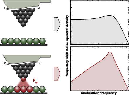
- centre position of the cantilever oscillation (see Figure 3). We explicitly include the amplitude dependency on the frequency shift Δf by including the oscillation amplitude component Az perpendicular to the sample surface. This dependency follows from the convolution of the interaction force with the
- . It is identical to −βts. The second term is a result from the convolution of the tip–sample force interaction with a weighting function [21]. For large oscillation amplitudes, a dependence has been found, allowing the definition of an amplitude-independent, normalised frequency shift [21]. This


![[Graphic 32]](/bjnano/content/inline/2190-4286-7-181-i73.png?max-width=637&scale=1.18182) wit...
wit...

![[Graphic 34]](/bjnano/content/inline/2190-4286-7-181-i75.png?max-width=637&scale=1.18182) wit...
wit...


Customized MFM probes with high lateral resolution
Beilstein J. Nanotechnol. 2016, 7, 1068–1074, doi:10.3762/bjnano.7.100

- an overestimation due to the tip–sample convolution effect). Both parameters were not found to change in great measure for the thickness range used to coat the AFM sensors. On the other hand, the MFM analysis demonstrates that the easy axis of this thin film remains mainly in-plane (IP) due to the


Thermo-voltage measurements of atomic contacts at low temperature
Beilstein J. Nanotechnol. 2016, 7, 767–775, doi:10.3762/bjnano.7.68

- the different reflectivity of gold and Kapton Cirlex there is an intensity profile corresponding to the convolution of a box function for the stripe and a 2D Gauss profile for the laser. It can be easily shown that the direction parallel to the stripe does not play any role, so the convolution reduces


In situ observation of deformation processes in nanocrystalline face-centered cubic metals
Beilstein J. Nanotechnol. 2016, 7, 572–580, doi:10.3762/bjnano.7.50

- regime is a convolution of film bending (indicated by the green line in the histogram) and crystallite rotation due to heterogeneous intergranular deformation, which is accommodated by GB-mediated processes (Figure 5). Twin and multiple twin activity (Σ3 and Σ9 activity) are observed in all Pd–Au alloys


Surface-site reactivity in small-molecule adsorption: A theoretical study of thiol binding on multi-coordinated gold clusters
Beilstein J. Nanotechnol. 2016, 7, 53–61, doi:10.3762/bjnano.7.6

- convolution of site reactivity and van der Waals attraction was found to determine the preference of methylthiolate to one or another binding site. As a result, adsorption was strongest at the kink sites (cf and fg), at edge sites where strong methyl-Au dispersive interactions could be established with the


Development of a novel nanoindentation technique by utilizing a dual-probe AFM system
Beilstein J. Nanotechnol. 2015, 6, 2015–2027, doi:10.3762/bjnano.6.205

- (motion in X and Y). The convolution of X and Y motion into the measurement cause overestimation errors in the interpretation of material properties using FD curves. Instrumented nanoindentation (INI) tools can be used for a large dynamic force range. However, the displacement and force sensitivity are
- process. Note that the AFM probe reflects only the true Z axis movement of the indenter probe unlike the conventional AFM systems where the measurement relies on laser deflection of the cantilever itself which includes a convolution of X and Y motion into the laser deflection reading. As it can be seen


Distribution of Pd clusters on ultrathin, epitaxial TiOx films on Pt3Ti(111)
Beilstein J. Nanotechnol. 2015, 6, 2007–2014, doi:10.3762/bjnano.6.204

- the measured particle diameter is actually the result of a convolution between the true particle size and the STM tip shape [14]. The actual particle diameter is smaller, but the distribution obtained for different coverages and the two different substrates still allow for comparison. Regarding the


