


Search results
Search for "electric potential" in Full Text gives 28 result(s) in Beilstein Journal of Nanotechnology.
Influence of an external electric field on the catalytic CO oxidation of nanoscaled CeO2 and its La3+ and Gd3+ congeners
Beilstein J. Nanotechnol. 2026, 17, 1028–1038, doi:10.3762/bjnano.17.70
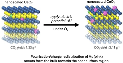
- potential, charge transport within nCeO2 is modulated. Our results show that both dopants Gd3+ and La3+ lead to an increasing VO concentration, whereas the impact of the applied potential on the oxidation behaviour varies with catalyst composition. The applied electric potential markedly improves the
- controlled by the underlying oxidic defect structure. Keywords: cerium oxide; CO oxidation; defect structure; doped cerium oxide; electric potential; Introduction Catalytic CO oxidation is a straightforward approach to reduce CO levels. A variety of catalysts have been synthesized and applied to improve
- negative bias (Pt: 4–8% and Pd: 4–12%) [14][15]. The catalytic decomposition of ammonia over organoboron nanoparticles was also examined under an external electric potential. Applying positive or negative potential allowed the decomposition rate to be tuned between +26% and −37% relative to the zero-bias


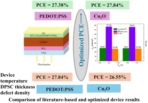
Comparison of organic and inorganic hole transport layers in double perovskite material-based solar cell
Beilstein J. Nanotechnol. 2025, 16, 119–127, doi:10.3762/bjnano.16.11
- equation is as follows [20]: where e is the electronic charge, ϕ is the electric potential, ε0 is the vacuum permittivity, εr is the relative permittivity, p(x) and n(x) are, respectively, hole and electron position dependence, ND is the shallow donor density, NA is the acceptor donor density, and ρp and


Electrospun nanofibers: building blocks for the repair of bone tissue
Beilstein J. Nanotechnol. 2024, 15, 941–953, doi:10.3762/bjnano.15.77
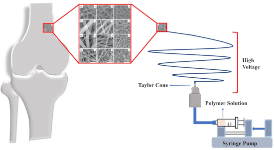
- electrospinning process because a stable Taylor cone can only form when the electric potential is high enough to overcome the surface tension of the solution [51][68][69][70]. The surface tension of the polymer liquid directly affects the critical stress; with increasing surface tension, the critical voltage


Plasmonic nanotechnology for photothermal applications – an evaluation
Beilstein J. Nanotechnol. 2023, 14, 380–419, doi:10.3762/bjnano.14.33
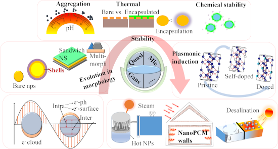
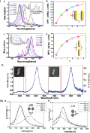
- radiation, is derived starting from Laplace’s equation with an electric potential (ϕ), Calculation of the resulting scalar potentials inside and outside the particle leads to the expression for the polarizability (α) of the particle, εm is the dielectric constant of the surrounding medium. The extinction




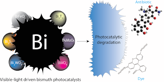
Bismuth-based nanostructured photocatalysts for the remediation of antibiotics and organic dyes
Beilstein J. Nanotechnol. 2023, 14, 291–321, doi:10.3762/bjnano.14.26
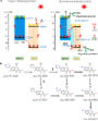
- holes and electrons. Charge carriers are oxidised and reduced at sites with reduced electric potential when they are separated by type-II heterojunctions, which, according to Low et al. [165], decreases the charge carrier separation efficiency and the redox ability of the photocatalyst. The shortcomings


Simulation of gas sensing with a triboelectric nanogenerator
Beilstein J. Nanotechnol. 2021, 12, 507–516, doi:10.3762/bjnano.12.41
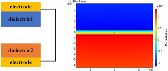
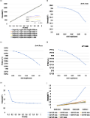
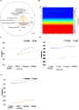
- the two dielectric materials varies, the field intensity caused by the charge also varies. The corresponding electric potential decreases with decreasing distance and increases with increasing distance. Figure 3b is the electric potential distribution diagram when the distance is 0.1 mm. In the
- difficult to directly test the influence of the shape of the triboelectric material on the electric potential due to the influence of various factors. Here, we set the shape of the upper triboelectric material to be an isosceles triangle and a right-angled triangle, the height is set to 1 mm, and the other
- parameters are the same as in Figure 2, as shown in Figure 4. The three models were simulated and compared in COMSOL while ignoring edge effects. As can be seen from Figure 5a–c, the electric potential of the rectangle and the isosceles triangles is symmetrically distributed along the central axis, while



Paper-based triboelectric nanogenerators and their applications: a review
Beilstein J. Nanotechnol. 2021, 12, 151–171, doi:10.3762/bjnano.12.12
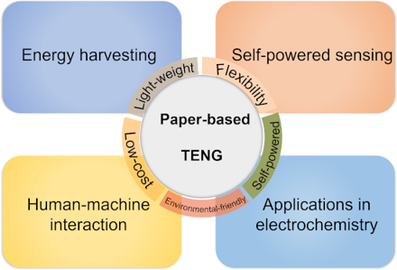
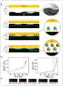
- negative charges) are induced by the same amount on the surfaces of the friction layers. As there is no electric potential at this stage, there is no electron transfer between the two conductive layers (Figure 2b-I). When the two friction layers start to separate along the vertical direction, opposite
- charges are induced in the upper and lower conductive electrodes owing to electrostatic induction (Figure 2b-II). As the distance between the two layers increases, the electric potential difference between the two layers enhances, driving the electrons to flow through the external load which generates an






Electrokinetic characterization of synthetic protein nanoparticles
Beilstein J. Nanotechnol. 2020, 11, 1556–1567, doi:10.3762/bjnano.11.138
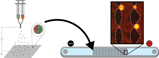
- driven processes are suitable for a wide range of applications due to their simplicity and robustness. An applied electric potential can be used to manipulate a biological particle and its surrounding liquid, since the electroosmotic (EO) flow can allow for an “on the fly” dynamic flow redirection within
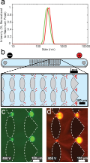
- , Supporting Information File 1). The particles are introduced at the inlet reservoir prior to applying an electric potential. In the devices, upon the application of an electric potential the particles will begin migrating in the device towards either the inlet or outlet reservoirs. The particles stop
- illustrated that by employing insulator-based EK microfluidics, it is possible to differentiate SPNPs by two distinct characteristics, that is, protein composition and anisotropy. The electric potential required to electrokinetically trap and enrich homogenous SPNPs depends on the particle composition (i.e



Prestress-loading effect on the current–voltage characteristics of a piezoelectric p–n junction together with the corresponding mechanical tuning laws
Beilstein J. Nanotechnol. 2019, 10, 1833–1843, doi:10.3762/bjnano.10.178
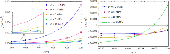
- I–V characteristics of p–n junctions are especially important. There is a steady current through a p–n junction when an electric bias voltage is applied. Because mechanical loadings can tune electric potential and electric field of a piezoelectric p–n junction, the corresponding I–V characteristics
- -electrostatic solutions [32]. Distributions of electric potential, electric field and carrier concentration are quasi-electrostatically solved in section “Quasi-electrostatic analysis of a mechanically loaded piezoelectric p–n junction under a bias voltage” for a piezoelectric p–n junction exposed to mechanical
- injection can be obtained in through two steps (Figure 1). (I) Electric potential and electric field in both the p-zone and the n-zone induced by static loadings can be solved from the electrostatic analysis in thermal equilibrium; (II) the steady diffusion of minority carriers can be studied by using a




Effects of surface charge and boundary slip on time-periodic pressure-driven flow and electrokinetic energy conversion in a nanotube
Beilstein J. Nanotechnol. 2019, 10, 1628–1635, doi:10.3762/bjnano.10.158
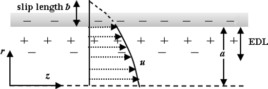
- Economics, Hohhot, China 10.3762/bjnano.10.158 Abstract Time-periodic pressure-driven slip flow and electrokinetic energy conversion efficiency in a nanotube are studied analytically. The slip length depends on the surface charge density. Electric potential, velocity and streaming electric field are
- 37.5 to 100 nm, and the bulk ionic concentration varies from 1 to 100 nm. The corresponding Debye length varies from 0.96 to 9.63 nm [29]. In this case, the overlap of EDLs is mild, and hence the electric potential within the nanotube can be described by the Poisson–Boltzmann equation [30]. In addition
- is the equilibrium distance of the Lennard–Jones potential, e is the elementary charge, lB = e2/(4πεkBT), kB is the Boltzmann constant, ε is the permittivity of the electrolyte solution and T is the absolute temperature [19][25]. The electric potential distribution φ in EDL satisfies the Poisson


Review of time-resolved non-contact electrostatic force microscopy techniques with applications to ionic transport measurements
Beilstein J. Nanotechnol. 2019, 10, 617–633, doi:10.3762/bjnano.10.62
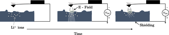
- force measurements to probe ionic transport. More specifically, these techniques are able to capture time-varying changes in the tip–sample coupling due to the movement of mobile ions within the sample in the sample volume directly underneath the probe tip. The ionic motion is initiated by an electric
- potential applied across the sample; the movement of mobile ions leads to a change in the tip–sample capacitance and, thus, to a change in the electrostatic force acting on the cantilever probe tip. The electrostatic tip–sample force is proportional to the capacitance gradient ∂C/∂z times the square of the





Exploring the photoleakage current and photoinduced negative bias instability in amorphous InGaZnO thin-film transistors with various active layer thicknesses
Beilstein J. Nanotechnol. 2018, 9, 2573–2580, doi:10.3762/bjnano.9.239
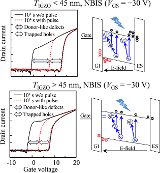
- active layer. In general, the electric potential exponentially declines inside the active layer and has a maximum transfer length called the Debye length. In terms of a-IGZO TFT, a Debye length of ≈40 nm is calculated based on a previous publication [30]. In case of a-IGZO TFT with the TIGZO = 25 nm, the
- positive VGS direction without SS degradation for the reverse measurement, as shown in Figure 4a. When the TIGZO is further increased to 75 and 100 nm, which is larger than the Debye length, the electric potential exponentially decreases inside the active layer under −30 V VGS bias. Although some amount of


Electrospun one-dimensional nanostructures: a new horizon for gas sensing materials
Beilstein J. Nanotechnol. 2018, 9, 2128–2170, doi:10.3762/bjnano.9.202
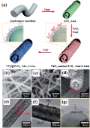
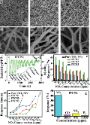
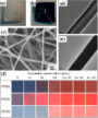
- sensing platforms (i.e., micro-electromechanical systems (MEMs)). The electrospinning process is governed by various parameters such as viscosity, conductivity, molecular weight of fiber components, surface tension of polymer solution, electric potential, working distance, and flow rate. Each parameter






Nonlinear effect of carrier drift on the performance of an n-type ZnO nanowire nanogenerator by coupling piezoelectric effect and semiconduction
Beilstein J. Nanotechnol. 2018, 9, 1917–1925, doi:10.3762/bjnano.9.183
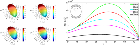
- establish the corresponding nonlinear governing equation of carrier concentration in this paper. The nonlinear accumulation of n-type carriers on one side of the ZNW cross section is shown in detail. Distribution characteristics of carrier concentration and electric potential in the cross section are
- discussed. Both the boundary electric charge and the boundary electric potential difference are calculated in depth. It is found that the amplitude of boundary electric charge always grows with increasing deformation, but the peaks of boundary electric charge do not appear directly at the cross-section
- , the electric potential should satisfy The point of zero electric potential is set at infinity, i.e., . The continuous conditions of normal electric displacement and electric potential at the boundary Ω, r = a, of the ZNW cross section require where refers to the electric potential within the ZNW


![[Graphic 46]](/bjnano/content/inline/2190-4286-9-183-i59.svg?max-width=637&scale=1.18182) and (b) boundary electric displacement Dr at Ω for different end f...
and (b) boundary electric displacement Dr at Ω for different end f...


Know your full potential: Quantitative Kelvin probe force microscopy on nanoscale electrical devices
Beilstein J. Nanotechnol. 2018, 9, 1809–1819, doi:10.3762/bjnano.9.172
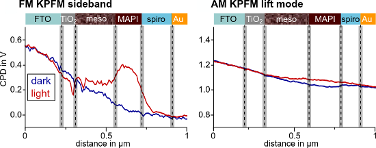
- electric potential landscape with local topographic information. Thus, KPFM is ideally suited to characterize of a variety of nanostructured semiconducting systems such as electronic devices [1] and solar cells [2]. To understand and improve the charge carrier generation and extraction within a solar cell


Robust midgap states in band-inverted junctions under electric and magnetic fields
Beilstein J. Nanotechnol. 2018, 9, 1405–1413, doi:10.3762/bjnano.9.133
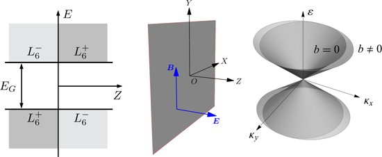
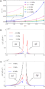
- /Δ, and . Notice that f/2 is the ratio between the electric potential drop across the spatial extent of the midgap states in the absence of fields and the magnitude of the fundamental gap 2Δ. Similarly, b is the square of the ratio between d and the magnetic length . Hereafter we shall consider b

![[Graphic 1]](/bjnano/content/inline/2190-4286-9-133-i26.svg?max-width=637&scale=1.18182) and
and ![[Graphic 2]](/bjnano/content/inline/2190-4286-9-133-i27.svg?max-width=637&scale=1.18182) band-edge profile of an abrupt band-inverted junction with aligned and same-sized gaps, l...
band-edge profile of an abrupt band-inverted junction with aligned and same-sized gaps, l...


![[Graphic 35]](/bjnano/content/inline/2190-4286-9-133-i60.svg?max-width=637&scale=1.18182) and b = 0.5 as a function of the electric field. It is important...
and b = 0.5 as a function of the electric field. It is important...

Electrical properties of a liquid crystal dispersed in an electrospun cellulose acetate network
Beilstein J. Nanotechnol. 2018, 9, 155–163, doi:10.3762/bjnano.9.18
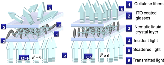
- Figure 12. After applying the electric potential between the metallic syringe tip and the plate, the fibers were deposited directly onto the ITO-coated glass, over the ITO surface. The fibers were then carefully dried in vacuum, at room temperature, for 72 h before further characterization and use. To


Electronic structure, transport, and collective effects in molecular layered systems
Beilstein J. Nanotechnol. 2017, 8, 2094–2105, doi:10.3762/bjnano.8.209
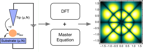
- , and Jνν' = Jν'ν is the Hund-rule coupling. The orbital energies eν are shifted by the electric potential, which is controlled by the bias voltage V = (μT − μS)/e. The eigenenergies and eigenstates of Hmol satisfy Only the differences between molecule and electrode energies enter the final results and


![[Graphic 29]](/bjnano/content/inline/2190-4286-8-209-i41.png?max-width=637&scale=1.18182) between the occupations nA and nB of the two checkerboard sublattices for a) asy...
between the occupations nA and nB of the two checkerboard sublattices for a) asy...

![[Graphic 30]](/bjnano/content/inline/2190-4286-8-209-i42.png?max-width=637&scale=1.18182) per site for a) asymmetric tunneling, Γtop/Γbottom = 0.5, and b) symmetric tunneli...
per site for a) asymmetric tunneling, Γtop/Γbottom = 0.5, and b) symmetric tunneli...
A comparative study of the nanoscale and macroscale tribological attributes of alumina and stainless steel surfaces immersed in aqueous suspensions of positively or negatively charged nanodiamonds
Beilstein J. Nanotechnol. 2017, 8, 2045–2059, doi:10.3762/bjnano.8.205
- and the sample was then immersed into 4 wt % oxalic acid solution maintained at 0 °C. A cathode was placed in the bath and an electric potential of 40 V was applied between the anode and the cathode. Anodization was halted at 3 min yielding an approximately 100 nm thick Al2O3 layer. After the


Spin-dependent transport and functional design in organic ferromagnetic devices
Beilstein J. Nanotechnol. 2017, 8, 1919–1931, doi:10.3762/bjnano.8.192
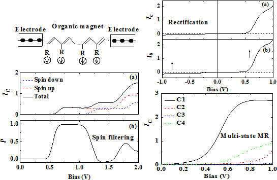
- transfer integral tmf. Since our focus is on effects coming from the bulk of the OF chain, we here assume spin-independent coupling between the OF and the electrodes. When a bias voltage V is applied, a spatially varying electric potential is generated along the molecule, which modifies both the electronic
- Hamiltonian involving the electric potential is Here, e is the electronic charge of an electron. The first term is the electric potential of the π-electrons, and the second term is the potential of the ion cores. Before calculating the transport properties, one needs to obtain the stationary structure of the


3D continuum phonon model for group-IV 2D materials
Beilstein J. Nanotechnol. 2017, 8, 1345–1356, doi:10.3762/bjnano.8.136
- 30) becomes because the spontaneous polarization Psp is constant in space. A solution of the combined system Equation 51–Equation 53 and Equation 56 with appropriate boundary conditions allows for the determination of the electric field (or electric potential ) and the displacements ux, uy and uz


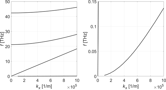
![[Graphic 19]](/bjnano/content/inline/2190-4286-8-136-i109.png?max-width=637&scale=1.18182) phonon modes of single-layer MoS2. The right plot is a ...
phonon modes of single-layer MoS2. The right plot is a ...
Analysis of self-heating of thermally assisted spin-transfer torque magnetic random access memory
Beilstein J. Nanotechnol. 2016, 7, 1676–1683, doi:10.3762/bjnano.7.160
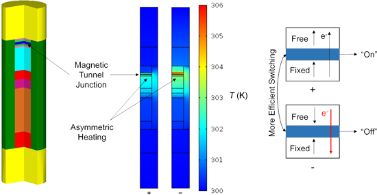
- external heat sources. Heat released or absorbed at the tunneling junction (Qt) is modeled using the probabilistic equation for hot tunneling carrier relaxation [1]: where is the magnitude of tunneling current density, Vt is the electric potential drop across the junction, λ is the inelastic scattering





Nonlinear thermoelectric effects in high-field superconductor-ferromagnet tunnel junctions
Beilstein J. Nanotechnol. 2016, 7, 1579–1585, doi:10.3762/bjnano.7.152
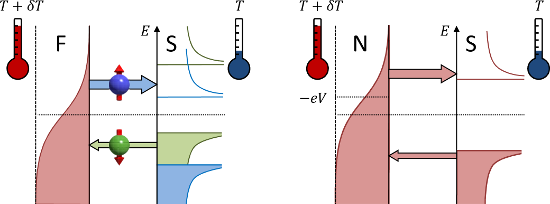
- the regime of linear response of the electric and thermal currents to the difference in electric potential or temperature [12][13][14]. In that case the linear response coefficients – electrical and thermal conductance, Seebeck and Peltier coefficients – are related by the famous Onsager symmetry


Multiscale modeling of lithium ion batteries: thermal aspects
Beilstein J. Nanotechnol. 2015, 6, 987–1007, doi:10.3762/bjnano.6.102
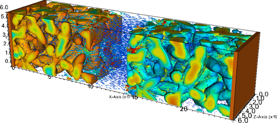
- temperature, the electric potential and the Li ion concentration, only. The pressure dependence can safely be neglected since it is only relevant in the double layer [27]. Also the possible dependence of the chemical potential on the electrical potential is usually not considered, since it is assumed that


Electronic and electrochemical doping of graphene by surface adsorbates
Beilstein J. Nanotechnol. 2014, 5, 1842–1848, doi:10.3762/bjnano.5.195
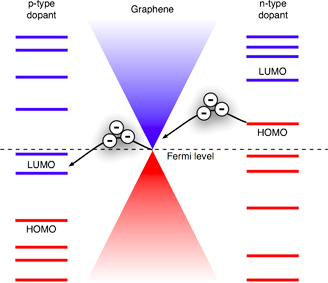
- charge carriers are induced by changing the electric potential between graphene and a gate, which can be, for example, a Si+/SiO2 substrate [1][13]. By varying the gate voltage, Vg, the type of carriers and their concentration in graphene can be tuned. The sign of the induced carriers is opposite to the





