Search results
Search for "feedback loop" in Full Text gives 83 result(s) in Beilstein Journal of Nanotechnology.
Charged particle single nanometre manufacturing
Beilstein J. Nanotechnol. 2018, 9, 2855–2882, doi:10.3762/bjnano.9.266


Low cost tips for tip-enhanced Raman spectroscopy fabricated by two-step electrochemical etching of 125 µm diameter gold wires
Beilstein J. Nanotechnol. 2018, 9, 2718–2729, doi:10.3762/bjnano.9.254

- removed from the near-field region of the sample, just excluding the feedback loop of the STM system. Vibrational bands of all molecules agree with the literature [60][61][62][63]. We finally apply our tips to obtain TERS spectra from the N-terminal domain of the Escherichia coli protein HypF (HypF-N
- oligomers when the STM feedback loop is on (red line) and when it is off (black line). Experimental conditions: λexc = 638 nm, P = 0.11 mW, t = 10 s. (a) STM image of Au(111) terraces on which R6G 10−4 M is adsorbed (∆V = 0.05 V – tip positive, current set point is 80 pA). The gray line indicates the zone


Dumbbell gold nanoparticle dimer antennas with advanced optical properties
Beilstein J. Nanotechnol. 2018, 9, 2188–2197, doi:10.3762/bjnano.9.205

- maintained with sub-nanometer accuracy to 2–4 nm by means of a force feedback loop regulating on the frequency shift of the force sensor, which is excited at its resonance frequency. The fluorescence emission rate as a function of the antenna–sample distance is recorded with the feedback loop switched off


The structural and chemical basis of temporary adhesion in the sea star Asterina gibbosa
Beilstein J. Nanotechnol. 2018, 9, 2071–2086, doi:10.3762/bjnano.9.196

- (Bruker Nano Inc., Santa Barbara, CA) using AFM in tapping mode. Tapping mode AFM was performed in amplitude modulation mode. The height of the cantilever position is constantly adjusted (via a feedback loop) to keep constant the ratio of the tip vibrational amplitude in contact with the sample surface to


Quantitative comparison of wideband low-latency phase-locked loop circuit designs for high-speed frequency modulation atomic force microscopy
Beilstein J. Nanotechnol. 2018, 9, 1844–1855, doi:10.3762/bjnano.9.176

- the conventional PLL design and their possible solutions. In the conventional design, a low-pass filter with relatively high latency is used in the phase feedback loop, leading to a slow response of the PLL. In the proposed design, a phase detector with a low-latency high-pass filter is located
- outside the phase feedback loop, while a subtraction-based phase comparator with negligible latency is located inside the loop. This design minimizes the latency within the phase feedback loop and significantly improves the PLL response speed. In addition, we implemented PLLs with the conventional and
- signal so that remains constant. In this way, the VCO, PC, and LF form a phase feedback loop, as illustrated in Figure 1. In a steady state, the frequency of the VCO output agrees with that of the PLL input. Thus, the VCO input changes in proportion to the frequency shift Δω of the PLL input. This


Know your full potential: Quantitative Kelvin probe force microscopy on nanoscale electrical devices
Beilstein J. Nanotechnol. 2018, 9, 1809–1819, doi:10.3762/bjnano.9.172

- ωE vanishes. In AM-KPFM, a feedback loop that minimizes the response amplitude by adjusting UDC. AM detection is ususally more prone to artifacts such cross coupling of the AC drive signal, e.g., into the shaker piezo [21]. Furthermore, Equation 3 shows that the amplitude of the electrostatic force


Direct AFM-based nanoscale mapping and tomography of open-circuit voltages for photovoltaics
Beilstein J. Nanotechnol. 2018, 9, 1802–1808, doi:10.3762/bjnano.9.171

- leverages photo-conducting AFM, along with an additional proportional-integral-derivative feedback loop configured to maintain open-circuit conditions while scanning. Alternating with short-circuit current mapping efficiently provides complementary insight into the highly microstructurally sensitive local
- energetic resolution unavoidably conflicts with experimental throughput. Accordingly, this work presents a new approach for directly mapping VOC with nanoscale resolution, requiring a single, standard-speed AFM scan. This leverages the concept of the proportional-integral-derivative (PID) feedback loop that
- underpins nearly all AFM topography imaging. Normally, this feedback loop continually updates the AFM probe height in order to maintain a constant AFM tip–sample interaction, which is sensed via the integrated cantilever deflection or amplitude that, of course, changes at surface protrusions or depressions


Lyapunov estimation for high-speed demodulation in multifrequency atomic force microscopy
Beilstein J. Nanotechnol. 2018, 9, 490–498, doi:10.3762/bjnano.9.47

- observables for the characterization of nanomechanical properties. Due to the large bandwidth requirements of tracking high frequencies in MF-AFM, every component of the z-axis feedback loop detailed in Figure 1 needs to be optimized for speed. This includes the lateral and vertical nanopositioner for each
- is shown to have a negative feedback loop in which integral action regulates the error. By feeding back an estimate of the input signal obtained from the parameterized states in the form of Equation 3, an error signal is generated. Regulation of this error through feedback leads to the much desired


The nanofluidic confinement apparatus: studying confinement-dependent nanoparticle behavior and diffusion
Beilstein J. Nanotechnol. 2018, 9, 301–310, doi:10.3762/bjnano.9.30

- background interference intensity and adjusts the height of the cover glass to keep the intensity constant. The feedback-loop can also operate during acquisition with a frequency of 20 Hz as illustrated by the red lines in Figure 2e. The blue lines indicate the measured laterally averaged gap distances for
- distance by 1 nm every 10th frame. (d) Effective gap distance variation Δd in the nanofluidic slit obtained from the local variation in optical path difference. (e) The height of the cover glass (red) is adjusted by a feedback loop to ensure a constant gap distance (blue) during experiments. (a) Contrast


Anchoring of a dye precursor on NiO(001) studied by non-contact atomic force microscopy
Beilstein J. Nanotechnol. 2018, 9, 242–249, doi:10.3762/bjnano.9.26

- of recording a first scan line with a closed feedback loop where the tip–sample distance is regulated using a topographic set point Δf1 and then acquiring a second scan in a open feedback loop following the recorded topography but applying an additional constant Z-offset, reducing the tip–sample


Combined scanning probe electronic and thermal characterization of an indium arsenide nanowire
Beilstein J. Nanotechnol. 2018, 9, 129–136, doi:10.3762/bjnano.9.15

- we detect modulations of the force gradient from the sidebands of the drive frequency fd in the deflection signal. The sidebands at fd ± fm are minimized by matching the dc tip bias to Ulcpd using a feedback loop. The sidebands at fd ± 2fm are proportional to the tip–sample capacitance gradient C
- ′′ and the KFM sensitivity. The feedback loop in our setup uses both pairs of sidebands and a Kalman filter to continuously estimate the surface potential and to avoid topographical artefacts [20]. Scanning thermal measurements of the InAs nanowire. (a) Setup for SThM measurements. (b) Topography and


A robust AFM-based method for locally measuring the elasticity of samples
Beilstein J. Nanotechnol. 2018, 9, 1–10, doi:10.3762/bjnano.9.1

- excitation of two cantilever eigenmodes [17][18][19][20][21], are performed in non-dry air, the instability of the tip–sample distance feedback loop, due to the use of the frequency shift as control parameter, makes the application of the method difficult if not impossible. However, despite these
- , two feedback loops for keeping the phase shifts 1 and 2 constant in order to track the contact resonances f1 and f2, and the last feedback loop as main feedback for controlling the applied normal force FN. Experimental Microscope and data acquisition The measurements were performed with a flex AFM
- of the Young’s modulus of the FDTS monolayer. Feedback loops necessary to track the flexural contact resonances of the cantilever. The main feedback loop ensures that the measurements are performed with a constant normal force. The other feedback loops are used to maintain constant values of phase 1


High-stress study of bioinspired multifunctional PEDOT:PSS/nanoclay nanocomposites using AFM, SEM and numerical simulation
Beilstein J. Nanotechnol. 2017, 8, 2069–2082, doi:10.3762/bjnano.8.207

- . The fundamental eigenmode is operated in amplitude modulation, i.e., there is a feedback loop modulating the oscillation amplitude for acquiring the topography of the sample, while the higher eigenmode (in this case the second eigenmode) is operated with constant excitation frequency and amplitude


Transport characteristics of a silicene nanoribbon on Ag(110)
Beilstein J. Nanotechnol. 2017, 8, 1699–1704, doi:10.3762/bjnano.8.170

- consisting of an SiNR, the STM tip and the Ag substrate. This method reduces the SiNR–Ag interaction and enables us to reveal the intrinsic features of SiNRs. The measurements were performed by a scheme summarized in Figure 3a. At first, the STM tip is fixed over one end of the SiNR while the STM feedback
- loop is turned off. Then we approach the tip to the target SiNR while measuring the conductance G at the sample voltage of 100 mV as a function of tip vertical position (Z). We set the position where the tip is fixed initially as Z = 0. Once the tip touches the target, we retract the tip to lift up the


Air–water interface of submerged superhydrophobic surfaces imaged by atomic force microscopy
Beilstein J. Nanotechnol. 2017, 8, 1671–1679, doi:10.3762/bjnano.8.167

- the data presented in Figure 3. However, the corresponding cross-section (Figure 5b, red line) contains two artifacts: the additional elevation at the pillar top is due to the feedback loop of the AFM system causing an overshoot in the height signal. The slope on the right, which seems to be too flat


High-speed dynamic-mode atomic force microscopy imaging of polymers: an adaptive multiloop-mode approach
Beilstein J. Nanotechnol. 2017, 8, 1563–1570, doi:10.3762/bjnano.8.158

- control mechanism applied [4][6]. Due to the time delay inevitably induced into the feedback loop for maintaining the RMS tapping amplitude during imaging, errors in tracking the sample topography can quickly result in loss of the tip–sample contact and annihilation of the probe tapping when the imaging
- -amplitude set-point to the free amplitude, Aset/Afree, based on a priori measured relation between dTM−d and (Adef/Afree) [1]. An online data-driven iterative feedforward controller is integrated to the RMS-z-feedback loop to enhance the sample topography tracking (Figure 9). Particularly, the feedforward
- ]. As the TM-deflection responds much faster than the RMS tapping-amplitude to the sample topography variation, so the inner-outer loop feedback control of the TM-deflection is faster than that of the RMS tapping amplitude. Moreover, the TM-deflection feedback loop facilitates the regulation of the


A review of demodulation techniques for amplitude-modulation atomic force microscopy
Beilstein J. Nanotechnol. 2017, 8, 1407–1426, doi:10.3762/bjnano.8.142

- used digital processing system. As a crucial bandwidth-limiting component in the z-axis feedback loop of an atomic force microscope, the purpose of the demodulator is to obtain estimates of amplitude and phase of the cantilever deflection signal in the presence of sensor noise or additional distinct
- nonlinear tip–sample forces acting on the cantilever, a feedback loop has to be employed in order to maintain a fixed setpoint with respect to the sample; the controller performs disturbance rejection by commanding a nanopositioner in its vertical direction. As the high-frequency cantilever deflection
- amplitude estimate as a function of the tracking bandwidth. The experimental analysis is concluded by high-speed constant-height tapping-mode AFM experiments which highlight the case where the demodulator is the bandwidth bottleneck in the z-axis feedback loop. Fundamentals of amplitude modulation and


Adsorption characteristics of Er3N@C80on W(110) and Au(111) studied via scanning tunneling microscopy and spectroscopy
Beilstein J. Nanotechnol. 2017, 8, 1127–1134, doi:10.3762/bjnano.8.114

- , with the bias voltage applied to the tip. The generated images were processed using WSxM [13]. The spatially resolved spectroscopy information was taken by I(U) measurements at open feedback loop at every pixel of the corresponding image. In order to obtain dI/dU(U) data a posterior numerical


Multimodal cantilevers with novel piezoelectric layer topology for sensitivity enhancement
Beilstein J. Nanotechnol. 2017, 8, 358–371, doi:10.3762/bjnano.8.38

- frequency shift of the cantilever’s motion correlate to properties of the sample [15]. When closing a feedback loop around these observables with the z-axis nanopositioner, the controller output is routinely used to map the surface topography of the sample. Recently, the additional excitation and detection


Noise in NC-AFM measurements with significant tip–sample interaction
Beilstein J. Nanotechnol. 2016, 7, 1885–1904, doi:10.3762/bjnano.7.181
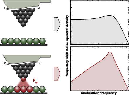
- increased due to a coupling of the phase-locked loop with the amplitude and the distance control loops. While noise in the amplitude control loop itself is essentially independent of the frequency shift noise without tip–sample interaction, amplitude and topography feedback loop noise are coupled into the
- ), the parameter βts can be obtained by using either the frequency shift set-point Δfset for the topography feedback or by the average frequency shift measured at the tip–sample distance zp with deactivated topography feedback loop. For the numerical evaluation of signal vs time traces and noise spectra
- and a significant slow-down of the step-response as shown in Figure 12 of appendix C. A small response time of the topography feedback loop causes a reduced noise in . Conclusions and System Optimisation We realise that the control and data acquisition system of a NC-AFM is a complex network of


![[Graphic 32]](/bjnano/content/inline/2190-4286-7-181-i73.png?max-width=637&scale=1.18182) wit...
wit...

![[Graphic 34]](/bjnano/content/inline/2190-4286-7-181-i75.png?max-width=637&scale=1.18182) wit...
wit...


Generalized Hertz model for bimodal nanomechanical mapping
Beilstein J. Nanotechnol. 2016, 7, 970–982, doi:10.3762/bjnano.7.89

- as amplitude-modulation (AM) AFM [18][19][20]), is one of the most commonly used parametric techniques, where the cantilever is driven on resonance and the cantilever–sample distance is adjusted by a feedback loop to maintain a constant oscillation amplitude at every image pixel. The time required


![[Graphic 4]](/bjnano/content/inline/2190-4286-7-89-i40.png?max-width=637&scale=1.18182) approximation applied to Equation 6 i...
approximation applied to Equation 6 i...


Large area scanning probe microscope in ultra-high vacuum demonstrated for electrostatic force measurements on high-voltage devices
Beilstein J. Nanotechnol. 2015, 6, 2485–2497, doi:10.3762/bjnano.6.258

- certain surface area. The tip height is controlled by a feedback loop correlating the tip–sample interaction with the deflection of the cantilever. However, the interaction force contains many different components which can only be partly suppressed (e.g., magnetic forces when inspecting non-magnetic


Sub-monolayer film growth of a volatile lanthanide complex on metallic surfaces
Beilstein J. Nanotechnol. 2015, 6, 2412–2416, doi:10.3762/bjnano.6.248

- temperature was kept at ≈5 K. The dI/dV spectra were taken using a standard lock-in amplifier technique with a 487 Hz modulation frequency and 20 mV modulation voltage with an open feedback loop. The dI/dV maps were recorded with the same lock-in parameters but with a closed feedback loop. A ball–stick model


Kelvin probe force microscopy for local characterisation of active nanoelectronic devices
Beilstein J. Nanotechnol. 2015, 6, 2193–2206, doi:10.3762/bjnano.6.225

- established technique that allows for the mapping of local electrostatic potentials with an atomic force microscope (AFM) [1][2][3]. In contrast to electrostatic force microscopy (EFM), which measures merely the effect of electrostatic forces on the oscillation of the tip, a feedback loop nullifies the
- on the number of layers. KFM has found widespread use in both vacuum and ambient environments. Most commercial instruments for operation in air include a scan mode based on amplitude modulation KFM (AM-KFM). In this mode, the feedback loop nullifies the cantilever oscillation that is excited by a
- shift Δf, exhibits a frequency component at the electrostatic modulation frequency, which is nullified by the Kelvin feedback loop. Frequency modulated KFM (FM-KFM) [16][17] thus provides a map of potentials required to minimise the electrostatic force gradient, proportional to Δf for small mechanical


![[Graphic 33]](/bjnano/content/inline/2190-4286-6-225-i48.png?max-width=637&scale=1.18182) for different modulation amplitu...
for different modulation amplitu...


Virtual reality visual feedback for hand-controlled scanning probe microscopy manipulation of single molecules
Beilstein J. Nanotechnol. 2015, 6, 2148–2153, doi:10.3762/bjnano.6.220

- tip was stabilized, the STM current feedback loop was opened and the control over the tip position was passed to the operator. The operator contacted the molecule by moving the tip in a strictly vertical trajectory (x,y tip coordinates frozen) until a sharp jump of the I and Δf bar indicators in the


