Search results
Search for "resolution" in Full Text gives 1176 result(s) in Beilstein Journal of Nanotechnology. Showing first 200.
Spatial mapping of photovoltage and light-induced displacement of on-chip coupled piezo/photodiodes by Kelvin probe force microscopy under modulated illumination
Beilstein J. Nanotechnol. 2023, 14, 1059–1067, doi:10.3762/bjnano.14.87

- mechanical oscillation of the piezoelectric membrane with vertical atomic resolution in real-time. This technique offers the opportunity to measure concurrently the optoelectronic and mechanical response of the device at the nanoscale. Furthermore, time-dependent atomic force microscopy (AFM) was employed to
- precise motion with high resolution. This offers promising possibilities for biomedical, environmental, and micro/nanoengineering applications [5][6]. Various types of design and actuation mechanisms have been developed in recent years [7][8]. A primary requirement to unlock the better performance of
- these micro/nano devices is to scrutinize their structure and the interaction between their different components. This can be done by high-resolution characterization techniques that simultaneously probe dynamic properties of different parts of the device. This enables the decoupling of the roles of


Exploring internal structures and properties of terpolymer fibers via real-space characterizations
Beilstein J. Nanotechnol. 2023, 14, 1004–1017, doi:10.3762/bjnano.14.83

- through real-space mapping. Complementing these full-fiber scans, high-resolution topography and stiffness maps on smaller fiber subdomains were also obtained to study the nanostructure of Technora®. From detailed topography maps, we found that the well-aligned surface features observed on the full
- on the AFM maps for clarity. In each highlighted region, there was clearly a correlation between topography and stiffness, but the precise nature of this correlation required higher resolution analysis of line profiles. From lateral profiles such as Figure 5a, we observed that domains with high
- structures of these fiber classes, which in turn help explain the mechanical and multifunctional performances of these fiber classes reported in other studies. In the future it would be especially interesting to carry out higher resolution scans within these fibers to characterize atomic structure [26]. Flat


Fragmentation of metal(II) bis(acetylacetonate) complexes induced by slow electrons
Beilstein J. Nanotechnol. 2023, 14, 980–987, doi:10.3762/bjnano.14.81

- of an electron source, an oven, and a quadrupole mass analyzer (QMA). The components are housed in a UHV chamber at a base pressure of around 2 × 10⁻⁸ mbar. A well-defined electron beam generated from a trochoidal electron monochromator (resolution approx. 210 meV FWHM), orthogonally intersects an


Isolation of cubic Si3P4 in the form of nanocrystals
Beilstein J. Nanotechnol. 2023, 14, 971–979, doi:10.3762/bjnano.14.80

- determination; thus, the linear dimensions of the particles could only be estimated to be in the range of 10–50 nm. The particles are polycrystalline and highly defective as evident from the high-resolution image (Figure 7a). The size of the crystalline domains does not exceed 10 nm in its longest dimension
- . (a) Bright-field TEM image and (b) electron diffraction of the sample SP550. TEM studies of the sample SP550. (a) High-resolution TEM image; (b) HAADF-STEM image; EDX elemental maps for (c) Si Kα, (d) P Kα, and (e) O Kα. The scale bar in images (b–e) is 30 nm. Synthesis conditions and results of X


Upscaling the urea method synthesis of CoAl layered double hydroxides
Beilstein J. Nanotechnol. 2023, 14, 927–938, doi:10.3762/bjnano.14.76

- microscope at an accelerating voltage of 20 kV. Atomic force microscopy (AFM) AFM was carried out with a Bruker Dimension Icon microscope in scan-assist-mode. A Bruker Scanasyst-Air silicon tip with a diameter of around 10 nm was used to obtain images with a resolution of 512 × 512 or 1024 × 1024 pixels. The
- aperture selecting the unscattered electrons. To record the images, an AMT RX80 8MP CCD camera (JEOL JEM-1010) and a Gatan CCD 1k × 1k device were used. (A) PXRD patterns exhibit the layered nature of the obtained samples. Indexation according to [13]. (B) ATR-FTIR spectra. (C) High-resolution XPS spectra


Two-dimensional molecular networks at the solid/liquid interface and the role of alkyl chains in their building blocks
Beilstein J. Nanotechnol. 2023, 14, 872–892, doi:10.3762/bjnano.14.72

- flat conducting substrates, such as metal surfaces and highly oriented pyrolytic graphite (HOPG), under ultrahigh vacuum (UHV) conditions, at solid/air or solid/liquid interfaces [23][24][25][26][27][28]. Although UHV-STM offers high-resolution imaging, it requires large, complex, and expensive
- resolution. (ii) Post-reaction is available by external stimuli such as the addition of metal ions for metal coordination, light irradiation for photoreaction, and post-blending of other molecules. (iii) The dynamic process of the 2D structural change (caused by the external stimuli) can be followed in situ


Industrial perspectives for personalized microneedles
Beilstein J. Nanotechnol. 2023, 14, 857–864, doi:10.3762/bjnano.14.70

- dollars (2500+ USD) when new, but these cost-effective printers are aimed at hobbyists and lack the resolution necessary for microneedle development (Figure 4). Professional SLA or DLP printers are more suitable for microneedle development because they can achieve feature sizes of the order of a few
- dimensions with high spatial resolution, which lends itself to continuous rather than discrete printing [59][61]. A key result of 2PP grayscale printing is that the technique is, on average, five to ten times faster than the common 2PP layer-by-layer approach [52]. Thiel et al. successfully applied 2GL® to


Nanostructured lipid carriers containing benznidazole: physicochemical, biopharmaceutical and cellular in vitro studies
Beilstein J. Nanotechnol. 2023, 14, 804–818, doi:10.3762/bjnano.14.66

- Fourier-transform infrared spectroscopy Fourier-transform infrared spectroscopy spectra were obtained. The attenuated total reflection mode was used to record the spectra over the range of 400–4000 cm−1 at a resolution of 2 cm−1. Transmission electron microscopy Transmission electron microscopy images


Silver-based SERS substrates fabricated using a 3D printed microfluidic device
Beilstein J. Nanotechnol. 2023, 14, 793–803, doi:10.3762/bjnano.14.65

- dimension to a scale smaller than a millimeter remains challenging [29]. In the second approach, 3D printing can replace photolithography to fabricate a mold. This approach can achieve a better lateral resolution of printed features down to 100 µm with a higher aspect ratio of the printed channel features
- [30]; also, it does not require a clean room. The stereolithography (SLA) technique is an additive manufacturing technique in which a photopolymer resin is cured and converted from a liquid to a solid by an ultraviolet laser. The resolution of SLA printers is determined by the radial beam scattering
- and the type of resin [31]. With particular resins, SLA can fabricate features with lateral dimensions of 100 µm and a mold-printed resolution of 50 µm. Over the past decade, numerous SERS substrates based on various materials, including paper [32][33], polymers [34][35], fibers [36], dielectrics [37


In situ magnesiothermic reduction synthesis of a Ge@C composite for high-performance lithium-ion batterie anodes
Beilstein J. Nanotechnol. 2023, 14, 751–761, doi:10.3762/bjnano.14.62

- carried out for structural and phase information. Infrared (IR, Shimadzu IRAffinity-1S) and Raman (LabRAM HR evolution confocal Raman microscope) spectra were measured for bond analysis. Field-emission scanning electron microscopy (FE-SEM, Hitachi S-4800) and high-resolution transmission electron


Cross-sectional Kelvin probe force microscopy on III–V epitaxial multilayer stacks: challenges and perspectives
Beilstein J. Nanotechnol. 2023, 14, 725–737, doi:10.3762/bjnano.14.59

- technique for the analysis of an InP/GaInAs(P) multilayer stack. KPFM reveals a strong dependence on the local doping concentration, allowing for the detection of the surface potential of layers with a resolution as low as 20 nm. The analysis of the surface potential allowed for the identification of space
- of the atomic force microscope (AFM) for the evaluation of the surface potential with nanometric resolution. KPFM is a valuable investigative approach for the study of work functions via the measurement of the contact potential difference VCPD, that is, the difference between the electrostatic
- evaluation of the spatial resolution of our KPFM setup under ambient conditions. The second objective is a full understanding of the VCPD results combined with a description of the principal factors that affect KPFM measurements with the application of Kelvin probe (KP) numerical modelling. This enables the


Titania nanoparticles for photocatalytic degradation of ethanol under simulated solar light
Beilstein J. Nanotechnol. 2023, 14, 616–630, doi:10.3762/bjnano.14.51

- spectral alignment of the binding energy (BE) scale was referenced to adventitious carbon at 284.8 eV [40][41]. Figure 4a shows the full survey scans of TO-250-a, TO-850-b, and commercial TiO2 (Degussa P25) samples, indicating the presence of the expected elements Ti, O, and C. The high-resolution XPS
- of the complex PL band at 400 nm, the resolution of which into the components requires another investigation. Oxygen and titanium vacancies have been found. These points defects are created most probably at the surface of the powder particles because in the HRTEM figures we do not see any dislocation
- diffraction (XRD) patterns, measured by an X-ray diffractometer Panalytical X’Pert MPD theta–theta, and the morphological properties were determined by transmission electron microscopy (TEM), high-resolution transmission electron microscopy (HRTEM), and selected-area electron diffraction (SAED) measurements


Suspension feeding in Copepoda (Crustacea) – a numerical model of setae acting in concert
Beilstein J. Nanotechnol. 2023, 14, 603–615, doi:10.3762/bjnano.14.50

- -resolution CLSM imaging or atomic force microscopy. As it was visualized by CLSM [55][56][57], the basal parts of some short and long setae appear to be relatively soft and seem to contain resilin or other proteins. This should influence the mobility of the rotating setae. To account for this in the


Thermal transport in kinked nanowires through simulation
Beilstein J. Nanotechnol. 2023, 14, 586–602, doi:10.3762/bjnano.14.49

- range, setting the extreme low and high values in the bends and knee corners to grey. This allows the colour scale to span the range in the angled segments with higher resolution at the cost of hiding the highest and lowest values. In so doing, a clear and unique phenomenon emerges in the PMC result for


Nanoarchitectonics to entrap living cells in silica-based systems: encapsulations with yolk–shell and sepiolite nanomaterials
Beilstein J. Nanotechnol. 2023, 14, 522–534, doi:10.3762/bjnano.14.43

- without staining. Electron microscopy imaging was conducted using a field-emission scanning electron microscope FEI-NOVA NanoSEM 230 equipped with an Apollo XL silicon drift detector from EDAX-Ametek or using a high-resolution JEOL IT500HR/LA microscope equipped with an energy dispersive X-ray


Molecular nanoarchitectonics: unification of nanotechnology and molecular/materials science
Beilstein J. Nanotechnol. 2023, 14, 434–453, doi:10.3762/bjnano.14.35

- include the direct observation of organic synthesis processes at the molecular level with high resolution, and the control of organic syntheses with probe microscope tips. These can also be considered as starting points for nanoarchitectonics. In this review, these examples of molecular nanoarchitectonics
- organic synthesis process at the molecular level with high resolution, and the control of organic synthesis with probe microscope tips. These examples are the fusion fields of nanotechnology and organic synthesis. This can also be considered as a starting point for nanoarchitectonics. In this review
- oligomeric chains were significantly elongated. High-resolution scanning tunneling microscope (STM) topography shows alternating bright twin spots, which correspond to phenylene and tetrafluorophenylene, respectively. A high-resolution atomic force microscope (AFM) image of an entirely elongated fine


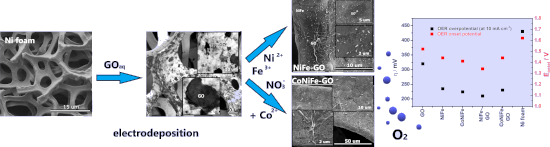
Evaluation of electrosynthesized reduced graphene oxide–Ni/Fe/Co-based (oxy)hydroxide catalysts towards the oxygen evolution reaction
Beilstein J. Nanotechnol. 2023, 14, 420–433, doi:10.3762/bjnano.14.34
- ]. The spectra were obtained using the total electron yield (TEY) detection mode, which can sample down to a depth of a few nanometers at room temperature. The beamline optics was optimized to perform the experiment with an energy resolution of 200 meV and better. X-ray diffraction (XRD) measurements
- calculations were determined based on the survey spectra collected in a wide range of binding energies, while valence state calculations were based on the high-resolution spectra. The C 1s peak (285.0 eV) was used to correct the results. Analysis of XPS spectra was performed with the Casa-XPS software using a
- ) deposited on nickel foam. SEM images and corresponding EDX maps of NiFe (a), NiFe-GO (b), CoNiFe (c), and CoNiFe-GO (d) deposited on nickel foam (error ≤ 0.5 atom %). Normalized XAS spectra (a–d) and XRD patterns (e) of NiFe, CoNiFe, NiFe-GO, and CoNiFe-GO. XPS high-resolution spectra of Ni 2p (a), Fe 2p (b


The steep road to nonviral nanomedicines: Frequent challenges and culprits in designing nanoparticles for gene therapy
Beilstein J. Nanotechnol. 2023, 14, 351–361, doi:10.3762/bjnano.14.30

- distributions can provide critical insights into the mechanisms of uptake and transfection. Alternatively, imaging flow cytometry combines the high-throughput nature of flow cytometry with a high degree of spatial resolution and has been recently developed and employed in nonviral gene delivery research [21
- intracellular trafficking [23]. In the absence of imaging flow cytometry, a two-pronged approach (high-resolution imaging plus a separate high-throughput analysis) is recommended to ensure the highest confidence in the result. Our literature assessment also revealed an increasing preference among the community
- complicated and sometimes ambiguous [32]. To circumvent these issues, given the advancement and prevalence of high- or super-resolution microscopy, imaging-based approaches can be used to directly visualize uptake and determine whether the NP is co-localized or associated with key endocytic structures or


Biocatalytic synthesis and ordered self-assembly of silica nanoparticles via a silica-binding peptide
Beilstein J. Nanotechnol. 2023, 14, 280–290, doi:10.3762/bjnano.14.25

- structures, high cost, labor-intensiveness, resolution limits, and high throughput time limit the scalability [8]. Self-assembly allows to circumvent some of the constraints of the top-down techniques to obtain ordered 2D or 3D nanostructures. Self-assembly, however, presents challenges of its own. One major


Recent progress in cancer cell membrane-based nanoparticles for biomedical applications
Beilstein J. Nanotechnol. 2023, 14, 262–279, doi:10.3762/bjnano.14.24

- advantages in better tissue penetration and spatial resolution [124]. Since US and PA commonly depend on the signal conversion of US transducers, the combination of US and PA dual-mode imaging shows good integration and enables the high-quality real-time imaging of tumors [125]. A biomimetic nanoagent with


Nanotechnology – a robust tool for fighting the challenges of drug resistance in non-small cell lung cancer
Beilstein J. Nanotechnol. 2023, 14, 240–261, doi:10.3762/bjnano.14.23

- also confirmed in an in vivo lung cancer mouse model [133]. Models for drug targeting via nanocarriers and ideas for the resolution of the main drawbacks regarding their performance are numerous. Only a choice of approaches was discussed in this section giving rational solutions for improving the


A novel approach to pulsed laser deposition of platinum catalyst on carbon particles for use in polymer electrolyte membrane fuel cells
Beilstein J. Nanotechnol. 2023, 14, 190–204, doi:10.3762/bjnano.14.19

- . The most important observation from the TEM analysis is that the PLD method allows for the deposition of PtNPs with even smaller dimensions than the size of PtNPs in the reference catalyst and with a denser distribution. EDX images taken with a spatial resolution of 160 pm confirm the presence of
- particles, which also correlates well with the TEM results (Figure 3). It also shows that the Pt-to-C ratio determined based on XPS measurements is inconsistent with the number of laser pulses used for Pt deposition on various carbon supports. The high-resolution spectra of the Pt 4f band of material A and
- spatial resolution of 160 pm using the HAADF (high-angle annular dark-field) detector. Statistical analysis was performed on the HRTEM images using the Digimizer software. About 200 particles were measured to assess their mean area and area distribution. For the measurement of the chemical composition of


High–low Kelvin probe force spectroscopy for measuring the interface state density
Beilstein J. Nanotechnol. 2023, 14, 175–189, doi:10.3762/bjnano.14.18

- of the effects of semiconductor interface states with high spatial resolution using high and low AC bias frequencies compared with the cutoff frequency of the carrier transfer between the interface and bulk states. Information on the energy spectrum of the interface state density is important for
- [1][2][3]. Therefore, direct observation of semiconductor surfaces with nanoscale spatial resolution will become even more important for understanding and controlling the effects of these properties on devices and for evaluating semiconductor device operation. Kelvin probe force microscopy (KPFM) is
- known as a method that can measure the contact potential difference (CPD) between a tip and a sample with high spatial resolution [4][5]. KPFM is based on the detection of the electrostatic force between a tip and a sample using atomic force microscopy (AFM) [6][7][8]. CPD and topographic measurements


Structural, optical, and bioimaging characterization of carbon quantum dots solvothermally synthesized from o-phenylenediamine
Beilstein J. Nanotechnol. 2023, 14, 165–174, doi:10.3762/bjnano.14.17

- to 4000 cm−1 with a spectral resolution of 4 cm−1. UV–vis spectra were recorded on a LLG-UNISPEC2 spectrophotometer (LLG, Germany) in the range of 190 to 900 nm at ambient temperature. The PL intensity measurements of CQDs and CQDs/PU composite samples were performed on a RF-5301PC spectrofluorometer


Formation of nanoflowers: Au and Ni silicide cores surrounded by SiOx branches
Beilstein J. Nanotechnol. 2023, 14, 133–140, doi:10.3762/bjnano.14.14

- annealed at 1050 °C was named 15Au5Ni. The morphology was imaged by optical microscopy (OM, Zeiss Axiotech) and high-resolution scanning electron microscopy (HR-SEM, Hitachi S-4800) equipped with energy-dispersive X-ray spectroscopy (EDS, Thermo Scientific). The SEM images were recorded by using mixed


