Search results
Search for "junction" in Full Text gives 316 result(s) in Beilstein Journal of Nanotechnology. Showing first 200.
Recent highlights in nanoscale and mesoscale friction
Beilstein J. Nanotechnol. 2018, 9, 1995–2014, doi:10.3762/bjnano.9.190

- patterns on a lattice-mismatched crystal overlayer [10][11][12]. One of the most frequent motivations to utilize FFM as a tool in nanotribology is its ability to mimic a single-asperity contact by the junction between a sharp AFM tip and the substrate. Such single-asperity contacts are widely considered as
- modulations were systematically obtained in the force channel, as shown in Figure 6b and Figure 6c. This indicates the formation of a well-defined tip–sample junction during the experiment. According to the authors, the tendency of the cyano end groups to form coordination bonds with Cu atoms of both the tip


Electromigrated electrical optical antennas for transducing electrons and photons at the nanoscale
Beilstein J. Nanotechnol. 2018, 9, 1964–1976, doi:10.3762/bjnano.9.187

- class of nanodevices enabling a bilateral transduction between electrons and photons. At the heart of the device is a tunnel junction that may either emit light upon injection of electrons or generate an electrical current when excited by a light wave. The current study explores a technological route
- and for interconnecting an electronic control layer to a photonic architecture. Keywords: electromigration; Fowler–Nordheim; hot-electron emission; inelastic electron tunneling; optical antennas; transition voltage; tunnel junction; Introduction The constant evolution of information technologies
- lithography, respectively. Each electrode is connected to a common ground (centered square) and can be individually addressed by a set of peripheral electrodes. To create a tunnel junction that will eventually form the active feedgap of an optical antenna, we perform an operator-controlled electromigration of


![[Graphic 32]](/bjnano/content/inline/2190-4286-9-187-i38.svg?max-width=637&scale=1.18182) and
and ![[Graphic 33]](/bjnano/content/inline/2190-4286-9-187-i39.svg?max-width=637&scale=1.18182) are...
are...


The role of the Ge mole fraction in improving the performance of a nanoscale junctionless tunneling FET: concept and scaling capability
Beilstein J. Nanotechnol. 2018, 9, 1856–1862, doi:10.3762/bjnano.9.177

- band-to-band quantum tunneling [25]. In this perspective, the tunnel current is generated near the source/channel junction and can be characterized by a transfer of electrons and holes across this junction. Hence, the tunneling current for an electron with longitudinal energy E and transverse energy ET
- the source/channel junction, respectively: where, EfSiGe and EfSi are the Fermi levels at the Si1−xGex source and Si channel regions, respectively, kB is the Boltzmann constant and T the temperature. In order to reflect accurately the device behavior for very short dimensions like in our case, the
- tunneling barrier width at the source/channel junction by varying the Ge concentration. Figure 3a shows the transfer characteristics associated of the proposed Si1−xGex/Si/Ge DG-HJ-JL TFET design with different Ge mole fractions. Increasing the Ge content leads to an increase of the drain current. This is


Direct AFM-based nanoscale mapping and tomography of open-circuit voltages for photovoltaics
Beilstein J. Nanotechnol. 2018, 9, 1802–1808, doi:10.3762/bjnano.9.171

- (Asylum Research MFP-3D-IO) is custom-mounted on an optical microscope (Nikon TE-2000) that has a broad-spectrum LED light source (Cree MK-R 12). The LED illuminates an area of ca. 1·104 µm2, including the sample/tip junction, from below through a 40× objective to provide an intensity of ca. 1 equivalent


A zero-dimensional topologically nontrivial state in a superconducting quantum dot
Beilstein J. Nanotechnol. 2018, 9, 1705–1714, doi:10.3762/bjnano.9.162

- simplest realization of such a 0D topological superconductor, i.e., a quantum dot [51][52][53][54] coupled with two superconducting leads in a magnetic Zeeman field, forming a superconductor–quantum dot–superconductor (SC–QD–SC) Josephson junction. Zero-energy modes and the corresponding CPR
- Hamiltonians, which read where t = tL = tR is the transparency of the dot–lead tunneling. We assume that the junction is symmetric and that the tunneling amplitudes do not depend on the electron momenta (wide band limit approximation). In the limit of a large superconducting gap, i.e., when the gap is larger
- specific values of the gauge-invariant phase φ = ±φ* where where |λ| < 1 if Bmin < |B| < Bmax. We will show that these gapless points define a topological phase transition in the system that corresponds to the appearance of discontinuous drops in the CPR of the junction. Figure 2 shows the single-particle


Josephson effect in junctions of conventional and topological superconductors
Beilstein J. Nanotechnol. 2018, 9, 1659–1676, doi:10.3762/bjnano.9.158

- end states. Using Green’s function techniques, the topological superconductor is alternatively described by the low-energy continuum limit of a Kitaev chain or by a more microscopic spinful nanowire model. We show that for the simplest S–TS tunnel junction, only the s-wave pairing correlations in a
- spinful TS nanowire model can generate a Josephson effect. The critical current is much smaller in the topological regime and exhibits a kink-like dependence on the Zeeman field along the wire. When a correlated quantum dot (QD) in the magnetic regime is present in the junction region, however, the
- Josephson current becomes finite also in the deep topological phase as shown for the cotunneling regime and by a mean-field analysis. Remarkably, we find that the S–QD–TS setup can support φ0-junction behavior, where a finite supercurrent flows at vanishing phase difference. Finally, we also address a multi


![[Graphic 75]](/bjnano/content/inline/2190-4286-9-158-i137.svg?max-width=637&scale=1.18182) = 1 in Figure 6, for different bulk Zeeman fields Vx (in meV) near the crit...
= 1 in Figure 6, for different bulk Zeeman fields Vx (in meV) near the crit...


Nanoscale electrochemical response of lithium-ion cathodes: a combined study using C-AFM and SIMS
Beilstein J. Nanotechnol. 2018, 9, 1623–1628, doi:10.3762/bjnano.9.154

- junction as another possible origin of modified transport characteristics. Especially in air, local anodic oxidation is well known to limit C-AFM capabilities and complicate the results interpretation in the case of silicon [16]. For this reason, UHV conditions have been investigated in order to increase


Robust topological phase in proximitized core–shell nanowires coupled to multiple superconductors
Beilstein J. Nanotechnol. 2018, 9, 1512–1526, doi:10.3762/bjnano.9.142

- superconductors. A non-zero phase difference was shown to stabilize the topological phase in a Josephson junction across a 2D electron gas with Rashba spin-orbit coupling and in-plane magnetic field [42] and in a topological insulator nanoribbon coupled with two superconductors [43]. Here, for concreteness, we


![[Graphic 30]](/bjnano/content/inline/2190-4286-9-142-i36.svg?max-width=637&scale=1.18182) ) = 0 and
) = 0 and ![[Graphic 31]](/bjnano/content/inline/2190-4286-9-142-i37.svg?max-width=637&scale=1.18182) = 0. The white areas are t...
= 0. The white areas are t...


![[Graphic 40]](/bjnano/content/inline/2190-4286-9-142-i46.svg?max-width=637&scale=1.18182) ) ≠ 0 and
) ≠ 0 and ![[Graphic 41]](/bjnano/content/inline/2190-4286-9-142-i47.svg?max-width=637&scale=1.18182) = 0. The white areas are topol...
= 0. The white areas are topol...

![[Graphic 50]](/bjnano/content/inline/2190-4286-9-142-i56.svg?max-width=637&scale=1.18182) ) ≠ 0 and
) ≠ 0 and ![[Graphic 51]](/bjnano/content/inline/2190-4286-9-142-i57.svg?max-width=637&scale=1.18182) 1 = 0,
1 = 0, ![[Graphic 52]](/bjnano/content/inline/2190-4286-9-142-i58.svg?max-width=637&scale=1.18182) 3 = π/2,
3 = π/2, ![[Graphic 53]](/bjnano/content/inline/2190-4286-9-142-i59.svg?max-width=637&scale=1.18182) 5 = −π/2. T...
5 = −π/2. T...

![[Graphic 65]](/bjnano/content/inline/2190-4286-9-142-i71.svg?max-width=637&scale=1.18182) ) ≠ 0 and
) ≠ 0 and ![[Graphic 66]](/bjnano/content/inline/2190-4286-9-142-i72.svg?max-width=637&scale=1.18182) 1 = π/2,
1 = π/2, ![[Graphic 67]](/bjnano/content/inline/2190-4286-9-142-i73.svg?max-width=637&scale=1.18182) 3 = −π/2,
3 = −π/2, ![[Graphic 68]](/bjnano/content/inline/2190-4286-9-142-i74.svg?max-width=637&scale=1.18182) 5 = π/2, and ...
5 = π/2, and ...


![[Graphic 79]](/bjnano/content/inline/2190-4286-9-142-i85.svg?max-width=637&scale=1.18182) = 3 of a triangular wi...
= 3 of a triangular wi...


Electronic conduction during the formation stages of a single-molecule junction
Beilstein J. Nanotechnol. 2018, 9, 1471–1477, doi:10.3762/bjnano.9.138

- , Kolkata 700 106, India 10.3762/bjnano.9.138 Abstract Single-molecule junctions are versatile test beds for electronic transport at the atomic scale. However, not much is known about the early formation steps of such junctions. Here, we study the electronic transport properties of premature junction
- configurations before the realization of a single-molecule bridge based on vanadocene molecules and silver electrodes. With the aid of conductance measurements, inelastic electron spectroscopy and shot noise analysis, we identify the formation of a single-molecule junction in parallel to a single-atom junction
- and examine the interplay between these two conductance pathways. Furthermore, the role of this structure in the formation of single-molecule junctions is studied. Our findings reveal the conductance and structural properties of premature molecular junction configurations and uncover the different


Cr(VI) remediation from aqueous environment through modified-TiO2-mediated photocatalytic reduction
Beilstein J. Nanotechnol. 2018, 9, 1448–1470, doi:10.3762/bjnano.9.137

- to the red end of the solar spectrum [162][163][164]. The p–n junction is formed by coupling a p-type (hole-rich) semiconductor with n-type (electron-rich) TiO2. As a result, the photoelectrons are diffused to the p-type semiconductor and holes are diffused to n-type TiO2 to create an inner electric
- water [165]. Upon increasing the content of Cu2O in TiO2/Cu2O nanocomposites, photoreduction increased and reached a maximum for 30% Cu2O. This is because 30% Cu2O might be an appropriate amount for the formation of a p–n junction between TiO2 and Cu2O nanoparticles, which could efficiently separate
- photocatalyst [173]. An increase in the surface area of NiO/TiO2 will lead to an increase of active sites, which enhances the photocatalytic activity. Ku et al. reported that coupling of p-type NiO with n-type TiO2 resulted in the development of an NiO/TiO2 photocatalyst with the formation of a p–n junction


Robust midgap states in band-inverted junctions under electric and magnetic fields
Beilstein J. Nanotechnol. 2018, 9, 1405–1413, doi:10.3762/bjnano.9.133

- presence of crossed electric and magnetic fields, the electric field being applied along the growth direction of a band-inverted junction. We show that the Dirac cone is robust and persists even if the fields are strong. In addition, we point out that Landau levels of electron states lying in the
- symmetry allow us to define a topological index given by the sign of the Dirac mass [21]. In 1994, Agassi studied the case of a band-inverted junction with a magnetic field applied parallel to the junction [23]. This author showed that the Dirac point remains robust upon the application of a magnetic field
- momentum perpendicular to the magnetic field is proportional to the position of the Landau orbits. If it becomes very large and the magnetic length is at the same time small, which happens for large magnetic fields, then the orbits do not intersect the junction and they might not notice that boundary

![[Graphic 1]](/bjnano/content/inline/2190-4286-9-133-i26.svg?max-width=637&scale=1.18182) and
and ![[Graphic 2]](/bjnano/content/inline/2190-4286-9-133-i27.svg?max-width=637&scale=1.18182) band-edge profile of an abrupt band-inverted junction with aligned and same-sized gaps, l...
band-edge profile of an abrupt band-inverted junction with aligned and same-sized gaps, l...


![[Graphic 35]](/bjnano/content/inline/2190-4286-9-133-i60.svg?max-width=637&scale=1.18182) and b = 0.5 as a function of the electric field. It is important...
and b = 0.5 as a function of the electric field. It is important...

Andreev spectrum and supercurrents in nanowire-based SNS junctions containing Majorana bound states
Beilstein J. Nanotechnol. 2018, 9, 1339–1357, doi:10.3762/bjnano.9.127

- the junction and two at the outer one. They hybridize and give rise to a finite energy splitting at a superconducting phase difference of π, a well-visible effect that can be traced back to the evolution of the energy spectrum with the Zeeman field: from the trivial phase with Andreev bound states
- in the junction. While this prediction has spurred a great deal of theoretical activity [25][26][27][28][29][30][31][32], experiments are still scarce [33], arguably due to the lack of good junctions until recently. The situation is now different and, since achieving high-quality interfaces is no
- also perform a systematic study of the phase-dependent supercurrents in the short- and long-junction limits. Due to finite length, the junction always hosts four MBSs in the topological regime. Apart from the MBSs located at the junction (inner MBSs), two extra MBSs are located at the nanowire ends


![[Graphic 44]](/bjnano/content/inline/2190-4286-9-127-i52.svg?max-width=637&scale=1.18182) in a short SNS j...
in a short SNS j...


![[Graphic 73]](/bjnano/content/inline/2190-4286-9-127-i81.svg?max-width=637&scale=1.18182) = 0 (a,b)...
= 0 (a,b)...


![[Graphic 84]](/bjnano/content/inline/2190-4286-9-127-i92.svg?max-width=637&scale=1.18182) ), fo...
), fo...


![[Graphic 119]](/bjnano/content/inline/2190-4286-9-127-i127.svg?max-width=637&scale=1.18182) at B = 1.5Bc. Contributions to the supercurrent for (a,b) short and ...
at B = 1.5Bc. Contributions to the supercurrent for (a,b) short and ...

![[Graphic 163]](/bjnano/content/inline/2190-4286-9-127-i171.svg?max-width=637&scale=1.18182) ), in (a,b) a short and (c,d) a long junction. (a,...
), in (a,b) a short and (c,d) a long junction. (a,...

![[Graphic 175]](/bjnano/content/inline/2190-4286-9-127-i183.svg?max-width=637&scale=1.18182) ), in (a,b) a...
), in (a,b) a...

![[Graphic 186]](/bjnano/content/inline/2190-4286-9-127-i194.svg?max-width=637&scale=1.18182) ) in (a,b) a short and (c,d) a long ...
) in (a,b) a short and (c,d) a long ...
The electrical conductivity of CNT/graphene composites: a new method for accelerating transmission function calculations
Beilstein J. Nanotechnol. 2018, 9, 1254–1262, doi:10.3762/bjnano.9.117

- X-axis and 2.13 nm along the Y-axis for each unit cell. Figure 5a shows the atomic structure of a pillared graphene film with an inter-tube distance of 2.1 nm. The tubes are connected seamlessly with graphene, i.e., the CNT smoothly passes into the graphene sheet, and the junction contains not only


Heterostuctures of 4-(chloromethyl)phenyltrichlorosilane and 5,10,15,20-tetra(4-pyridyl)-21H,23H-porphine prepared on Si(111) using particle lithography: Nanoscale characterization of the main steps of nanopatterning
Beilstein J. Nanotechnol. 2018, 9, 1211–1219, doi:10.3762/bjnano.9.112

- functionalized phthalocyaninato-polysiloxane was studied with STM on surfaces of highly oriented pyrolytic graphite (HOPG) by Samori et al. [22]. Photoelectronic devices of porphyrin polymers containing oligothienyl bridges were prepared as microscopic junction chips and as layered diodes by Shimadzu et al. [23


Semi-automatic spray pyrolysis deposition of thin, transparent, titania films as blocking layers for dye-sensitized and perovskite solar cells
Beilstein J. Nanotechnol. 2018, 9, 1135–1145, doi:10.3762/bjnano.9.105

- ), solid state dye-sensitized solar cells (SSDSSCs) and perovskite solar cells (PSCs) are attractive alternatives to solid state photovoltaics at competitive cost. The general concept of a DSSC is based on a liquid junction photo-electrochemical cell with a nanocrystalline TiO2 photoanode that is


Room-temperature single-photon emitters in titanium dioxide optical defects
Beilstein J. Nanotechnol. 2018, 9, 1085–1094, doi:10.3762/bjnano.9.100

- optical fibre (FO), which acts as the confocal pinhole. The fluorescence signal is fibre-optically split 50:50 (BS) incident upon two avalanche photodiodes (APD1,2, Perkin Elmer SPCM-AQRH-14-FC: timing resolution = 350 ps at 825 nm). The system can be switched (orange junction) between two main


Review on nanoparticles and nanostructured materials: history, sources, toxicity and regulations
Beilstein J. Nanotechnol. 2018, 9, 1050–1074, doi:10.3762/bjnano.9.98


Scanning speed phenomenon in contact-resonance atomic force microscopy
Beilstein J. Nanotechnol. 2018, 9, 945–952, doi:10.3762/bjnano.9.87

- velocity Vs. The adsorbed water layer is surrounding the tip–sample junction but does not exist in the contact region. This case, depicted in Figure 1b, represents a situation where the AFM is solely measuring the elastic properties of the sample. The elasticity of the sample has been represented as the


Cyclodextrin inhibits zinc corrosion by destabilizing point defect formation in the oxide layer
Beilstein J. Nanotechnol. 2018, 9, 936–944, doi:10.3762/bjnano.9.86
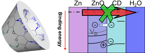
- interface, closely resembling the energy level alignment in an n–p junction. The energy level shift is too large to permit further electron transfer through the layer, inhibiting corrosion. Adsorption hence changes the defect density in the protecting ZnO layer. This mechanism of corrosion inhibition shows
- interface, making the interface behave similarly to an n–p junction. Charge transport is hence only possible from the n-type ZnO to β-CD, which behaves like a p-type layer, effectively blocking the anodic reaction. Most decisively, the energy level shift induced by the changes in the defect chemistry


Facile synthesis of a ZnO–BiOI p–n nano-heterojunction with excellent visible-light photocatalytic activity
Beilstein J. Nanotechnol. 2018, 9, 789–800, doi:10.3762/bjnano.9.72

- heterojunctions could promote increased photocatalytic activity efficiency. Once the p–n junction has been formed, the inner electric field between the inner surface of two semiconductors will promote the separation efficiency of photoinduced electron–hole pairs [30][31]. Consequently, coupling an n-type metal


Mechanistic insights into plasmonic photocatalysts in utilizing visible light
Beilstein J. Nanotechnol. 2018, 9, 628–648, doi:10.3762/bjnano.9.59

- characteristic features of the noble metal nanomaterials. Moreover, the formation of interfaces between noble metal particles and semiconductor materials further results in the formation of a Schottky junction. Thereby, the plasmonic characteristics have opened up a new direction in promoting an alternative path
- amalgamation of noble and semiconductor metal forms an exclusive “plasmonic photocatalyst” classification. The term “plasmonic” is mainly in reference to the unique characteristics of LSPR and induced effects [6]. However, the formation of a Schottky junction does not classify as plasmonic or resonant effects
- , and electronic interactions between the stabilizing ligands and nanoparticles [11]. Besides, the creation of a Schottky junction with a noble metal and a semiconductor acts to retard the recombination rate of electrons and holes [12]. LSPR takes place when noble metal NPs are excited by the


Revealing the interference effect of Majorana fermions in a topological Josephson junction
Beilstein J. Nanotechnol. 2018, 9, 520–529, doi:10.3762/bjnano.9.50

- the local density of states (DOS) in a topological Josephson junction. We show that the well-known 4π Josephson effect originates from the interference effect between two Majorana fermions (MFs) that are localized at the Josephson junction. In addition, the DOS for electrons (holes) shows the 4π
- DOS can be detected by using two STM leads or two normal leads. A single side lead can only detect the Andreev reflection tunneling process in the junction, which cannot reveal information about the interference effect in general. However, using two side leads, we can reveal information about the
- combined to form a topological Josephson junction (Top-JJ), the period of the supercurrent is 4π if MFs exist at the ends of both wires. This is different from the trivial case without MFs. In the trivial case in which only Cooper pairs can tunnel, the period is 2π. Since MFs have only half a degree of


Dopant-stimulated growth of GaN nanotube-like nanostructures on Si(111) by molecular beam epitaxy
Beilstein J. Nanotechnol. 2018, 9, 146–154, doi:10.3762/bjnano.9.17

- ]. The fabrication of a simple SC based on GaN NWs on Si(111) can be obtained via proper NW doping and formation of a p–n junction at Si substrate–GaN NW interface. Recently it has been theoretically demonstrated that optimization of the doping level and NW array morphology can lead to a power conversion


Comparative study of post-growth annealing of Cu(hfac)2, Co2(CO)8 and Me2Au(acac) metal precursors deposited by FEBID
Beilstein J. Nanotechnol. 2018, 9, 91–101, doi:10.3762/bjnano.9.11

- storage, ferroelectric tunnel junction memristors, metal interconnects for high performance integrated circuits in microelectronics and nano-optics applications, especially in the areas of plasmonics and metamaterials. Focused-electron-beam-induced deposition (FEBID) is a maskless direct-write tool


Beyond Moore’s technologies: operation principles of a superconductor alternative
Beilstein J. Nanotechnol. 2017, 8, 2689–2710, doi:10.3762/bjnano.8.269

- a deep analogy between superconducting logic cells and von Neuman cellular automata [16] where short-range interactions are predominant. The nonlinear element in superconducting circuits is the Josephson junction. It is a weak link between two superconductors, e.g., the most commonly used
- superconductor–isolator–superconductor (SIS) sandwich structure. One of the most important parameters of a Josephson junction is its critical current, Ic. This is the maximum superconducting current capable of flowing through the junction. A Josephson junction can be switched from the superconducting to the
- resistive state by increasing the current above Ic. The transition to the resistive state allows one to change the magnetic flux in a superconducting loop, and hence to perform a digital logic operation. The dynamics of a SIS junction is commonly described in the frame of the resistively shunted junction


