Search results
Search for "deposition" in Full Text gives 1162 result(s) in Beilstein Journal of Nanotechnology. Showing first 200.
A combined gas-phase dissociative ionization, dissociative electron attachment and deposition study on the potential FEBID precursor [Au(CH3)2Cl]2
Beilstein J. Nanotechnol. 2023, 14, 1178–1199, doi:10.3762/bjnano.14.98

- Iceland, Dunhagi 3, 107 Reykjavík, Iceland Inorganic and Organometallic Chemistry, Universität Erlangen-Nürnberg, 91058 Erlangen, Germany Carl Zeiss SMT GmbH, 64380 Roßdorf, Germany 10.3762/bjnano.14.98 Abstract Motivated by the potential of focused-electron-beam-induced deposition (FEBID) in the
- that we attribute to electron-induced secondary and tertiary reactions in the deposition process. We find this precursor to be stable at ambient conditions and to have sufficient vapor pressure to be suitable for use in HV instruments. More importantly, in the UHV setup, FEBID with [Au(CH3)2Cl]2
- yielded deposits with high gold content, ranging from 45 to 61 atom % depending on the beam current and on the cleanliness of the substrates surface. Keywords: dissociative electron attachment; dissociative ionization; focused-electron-beam-induced deposition (FEBID); gold deposit; low-energy electrons


Spatial variations of conductivity of self-assembled monolayers of dodecanethiol on Au/mica and Au/Si substrates
Beilstein J. Nanotechnol. 2023, 14, 1169–1177, doi:10.3762/bjnano.14.97

- deposition can be made. Overall, five areas were investigated on Au/mica and three for Au/Si, which all showed consistent images. Dodecanethiol SAMs on Au/mica Figure 3 shows images of the DDT-covered Au/mica surface obtained after the deposition procedure described above. In total, four different areas on
- . All these indications lead to the conclusion that ordered DDT SAMs form on the surface with the chosen deposition technique. More importantly, the current maps in Figure 3 show that substrate and measurement technique are suitable for obtaining information on the conductivity of a molecular SAM, as
- variation in the current is governed by the structure of the substrate, which remains qualitatively unchanged by the deposition of the SAM. For the Au/Si substrate, the rough topography yields only small areas on the surface on which comparable conductive properties can be expected. Without information on


A multi-resistance wide-range calibration sample for conductive probe atomic force microscopy measurements
Beilstein J. Nanotechnol. 2023, 14, 1141–1148, doi:10.3762/bjnano.14.94

- standard photolithography, using a mask aligner (MA6, Karl Suss, Germany), and conventional deposition techniques. Following a resist (about 1 µm thick) development process, a 2 inch diameter wafer was placed in a vacuum chamber for electron beam deposition of a 200 nm thick titanium/gold layer


Properties of tin oxide films grown by atomic layer deposition from tin tetraiodide and ozone
Beilstein J. Nanotechnol. 2023, 14, 1085–1092, doi:10.3762/bjnano.14.89

- Kristjan Kalam Peeter Ritslaid Tanel Kaambre Aile Tamm Kaupo Kukli Institute of Physics, University of Tartu, W. Ostwaldi 1, 50411 Tartu, Estonia 10.3762/bjnano.14.89 Abstract Polycrystalline SnO2 thin films were grown by atomic layer deposition (ALD) on SiO2/Si(100) substrates from SnI4 and O3
- implied the formation of single-phase oxide in the films grown at temperatures above 300 °C. Appropriateness of the mentioned precursor system to the preparation of SnO2 films was established. Keywords: atomic layer deposition; tin oxide; tin tetraiodide; Introduction Atomic layer-deposited SnO2 films
- precursor combinations for obtaining SnO2 in atomic layer deposition (ALD) processes [9]. Two of these processes have employed SnI4 as the metal precursor with either O2 [10][11][12][13][14] or H2O2 [10][11][15] as oxidizer. Of these two oxygen sources, O2 would be more desirable because with it a hydrogen


Spatial mapping of photovoltage and light-induced displacement of on-chip coupled piezo/photodiodes by Kelvin probe force microscopy under modulated illumination
Beilstein J. Nanotechnol. 2023, 14, 1059–1067, doi:10.3762/bjnano.14.87

- × 2.8) and (1.4 × 1.2) mm2 labeled as A, B, C, and D, respectively. In the process of fabrication, a 100 nm thick layer of LNO as the bottom electrode was first deposited, using pulsed laser deposition (PLD) technique, on a single crystal silicon wafer. Then, an 850 nm lead barium zirconia titanate


Nanoarchitectonics of photothermal materials to enhance the sensitivity of lateral flow assays
Beilstein J. Nanotechnol. 2023, 14, 988–1003, doi:10.3762/bjnano.14.82

- diagnostic tools. Based on the photothermal principle, very recently, Shirshahi et al. developed LFA strips for the detection of E. coli O157:H7 strains of bacteria. They used reduced graphene oxide as both tracer and photothermal signal amplification material. After the deposition of rGO on the test line


Fragmentation of metal(II) bis(acetylacetonate) complexes induced by slow electrons
Beilstein J. Nanotechnol. 2023, 14, 980–987, doi:10.3762/bjnano.14.81

- attachment. The reported data may contribute to a better understanding of the physical chemistry underlying the electron–molecule interactions, which is crucial for potential applications of these molecular systems in the deposition of nanoscale structures. Keywords: dissociative electron attachment; gas
- electron beam with an organometallic target (e.g., focused electron beam-induced deposition, FEBID) is a promising technique for direct 3D deposition of high-purity materials with minimum residual carbon in the product on the surface [4][5]. The FEBID precursor molecules adsorb and diffuse on the surface
- . Metal bis(acetylacetonate) complexes are of interest for many thin film fabrication techniques (e.g., chemical vapor deposition [9], atomic layer epitaxy [10], or atomic layer etching [11]) and as precursors for carbon materials, such as carbon nanotubes and carbon onion particles [12], or metal oxide


Isolation of cubic Si3P4 in the form of nanocrystals
Beilstein J. Nanotechnol. 2023, 14, 971–979, doi:10.3762/bjnano.14.80

- 520.8 cm−1. Interestingly, the observed Raman spectrum for SP900 is very similar to that of the product of silicon and phosphorus MBE co-deposition at 3:2 molar ratio [34]. This substance was reported as amorphous; however, it could contain Si3P4 NPs along with other SixPy compounds. Factor group
- Si3P4 phase. Also worth noting was that the synthesis of cubic Si3P4 NPs could be performed immediately after laser-induced or plasma-enhanced chemical vapor deposition of nanosilicon from the silane precursor (since the NPs obtained this way are readily hydrogenated). Additionally, there is preliminary
- (reagent grade) were used for sol preparation; 40% hydrofluoric acid (pure) was used for etching. Si NPs were synthesized by laser-induced chemical vapor deposition using a silane precursor (the average particle diameter was 20 nm [41]). The NPs oxidized when stored in air, and the resultant mass fraction


Low temperature atomic layer deposition of cobalt using dicobalt hexacarbonyl-1-heptyne as precursor
Beilstein J. Nanotechnol. 2023, 14, 951–963, doi:10.3762/bjnano.14.78

- , Clemens-Winkler-Str. 6c, 09116 Chemnitz, Germany FAP Forschungs- und Applikationslabor Plasmatechnik GmbH, Gostritzer Str. 67B, 01217 Dresden, Germany 10.3762/bjnano.14.78 Abstract In this work, we present the development of an atomic layer deposition (ALD) process for metallic cobalt. The process
- operates at low temperatures using dicobalt hexacarbonyl-1-heptyne [Co2(CO)6HC≡CC5H11] and hydrogen plasma. For this precursor an ALD window in the temperature range between 50 and 110 °C was determined with a constant deposition rate of approximately 0.1 Å/cycle. The upper limit of the ALD window is
- defined by the onset of the decomposition of the precursor. In our case, decomposition occurs at temperatures of 125 °C and above, resulting in a film growth in chemical vapour deposition mode. The lower limit of the ALD window is around 35 °C, where the reduction of the precursor is incomplete. The


Upscaling the urea method synthesis of CoAl layered double hydroxides
Beilstein J. Nanotechnol. 2023, 14, 927–938, doi:10.3762/bjnano.14.76

- spin-coated on a Si wafer (3000 rpm, 40 s), washed with ethanol and dried afterward. For AFM, the samples were diluted in ethanol and drop-cast on a Si/SiO2 wafer. Si/SiO2 wafers were washed by spin-coating ten droplets of acetone and ten droplets of isopropanol prior to sample deposition. Scanning


Ultralow-energy amorphization of contaminated silicon samples investigated by molecular dynamics
Beilstein J. Nanotechnol. 2023, 14, 834–849, doi:10.3762/bjnano.14.68

- years, the need to control what happens at the surface of the sample has risen sharply, specifically for semiconductors [3][4], microelectronics [5], and surface patterning [6][7]. Other applications of low-energy beams include the preparation of nanoholes [8][9]. Furthermore, deposition processes are


Silver-based SERS substrates fabricated using a 3D printed microfluidic device
Beilstein J. Nanotechnol. 2023, 14, 793–803, doi:10.3762/bjnano.14.65

- submerged in concentrated HNO3, rinsed with deionized water, and then dried at room temperature to produce the PS substrates. Fabrication of the SERS substrate The deposition of Ag particles on the substrates is based on the SAM method. Colloidal Ag NPs solutions were generated at the methanol/air interface
- homogeneous results because of the even deposition of the self-assembled monolayer of Ag NPs on the PS substrate. Detection of melamine using PS@Ag SERS substrate SERS spectra of MLM solutions at different concentrations (10−7 to 10−3 M) on the PS@Ag substrates were recorded, as shown in Figure 6a. The Raman


In situ magnesiothermic reduction synthesis of a Ge@C composite for high-performance lithium-ion batterie anodes
Beilstein J. Nanotechnol. 2023, 14, 751–761, doi:10.3762/bjnano.14.62

- preparation routes, such as sputtering deposition [20], wet-chemical reduction [21][22], thermal reduction [23], colloidal synthesis [24], and molten-salt synthesis [25], metallothermic, especially magnesiothermic reduction, has been widely applied in the synthesis of group-IV elements to control the


Control of morphology and crystallinity of CNTs in flame synthesis with one-dimensional reaction zone
Beilstein J. Nanotechnol. 2023, 14, 741–750, doi:10.3762/bjnano.14.61

- . To date, many researchers have shown promising results on the synthesis control of CNTs to produce tailored CNT morphologies and properties through conventional furnace-based methods. Progress in CNT synthesis processes has been achieved mostly using chemical vapor deposition (CVD). Various studies
- widely accepted vapor–liquid–solid mechanism, the growth of CNTs occurs in three steps, namely, melting of nickel particles, adsorption of carbon atoms onto the surface of the metallic nickel, and finally, diffusion and deposition of the precipitated carbon, which forms tubular materials by curling of
- large average CNT diameter with high standard deviation suggests different sizes of formed particles, possibly due to the high temperature. Generally, the size of nanoparticles is affected by several factors, including solution concentration, deposition method, quantity, and annealing [25]. At higher


Metal-organic framework-based nanomaterials as opto-electrochemical sensors for the detection of antibiotics and hormones: A review
Beilstein J. Nanotechnol. 2023, 14, 631–673, doi:10.3762/bjnano.14.52


ZnO-decorated SiC@C hybrids with strong electromagnetic absorption
Beilstein J. Nanotechnol. 2023, 14, 565–573, doi:10.3762/bjnano.14.47

- provide locations for the deposition of Zn2+ via electrostatic interactions. Cao et al. [26] have reported the growth of ZnO particles on MWCNTs through a similar mechanism. However, in their case, the functional groups on the MWCNTs were obtained by ultrasonic treatment in concentrated nitric acid. Four
- locations for the deposition of Zn2+ by electrostatic interactions. SCZ1 exhibits the best EM absorption properties. Its values for RLmin and EAB reach −65.4 dB and 7 GHz (10.96–17.96 GHz), respectively, at a small sample thickness and 30 wt % filler load. The effective EM absorption is related to the


SERS performance of GaN/Ag substrates fabricated by Ag coating of GaN platforms
Beilstein J. Nanotechnol. 2023, 14, 552–564, doi:10.3762/bjnano.14.46

- substrates using pulsed laser deposition (PLD) and magnetron sputtering (MS) and their evaluation as potential substrates for surface-enhanced Raman spectroscopy (SERS) are reported. Ag layers of comparable thicknesses were deposited using PLD and MS on nanostructured GaN platforms. All fabricated SERS
- : GaN/Ag; magnetron sputtering; nanofabrication; pulsed laser deposition; SERS substrates; surface-enhanced Raman spectroscopy (SERS); Introduction Surface-enhanced Raman spectroscopy (SERS) is a highly sensitive and specific technique with multiplexing capabilities [1][2][3][4]. It is considered for
- physical vapor deposition (PVD) methods have been tested to replace MS in coating GaN platforms with plasmonic metals. Pulsed laser deposition (PLD) is an interesting and still not fully explored alternative for the fabrication of SERS substrates [37][38]. Hence, our studies reported herein aimed to


On the use of Raman spectroscopy to characterize mass-produced graphene nanoplatelets
Beilstein J. Nanotechnol. 2023, 14, 509–521, doi:10.3762/bjnano.14.42

- extinction at 660 nm and using an extinction coefficient of 4237 mL·mg−1·m−1 [28] yielded a concentration of 0.028 mg·mL−1. To characterize the thickness of the particles in GNPref, the dispersion was drop-cast on to a cleaned Si/SiO2 (300 nm thick oxide layer) wafer. Before deposition, the dispersion was


Molecular nanoarchitectonics: unification of nanotechnology and molecular/materials science
Beilstein J. Nanotechnol. 2023, 14, 434–453, doi:10.3762/bjnano.14.35

- synthesize 8-carbon armchair graphene nanoribbons and nanographene C66 with periodic vacancies on the surface (Figure 8) [124]. Detailed processes of the surface synthesis of 5,8-dibromobenzene molecules kept at room temperature after deposition on Au(111) were disclosed through STM observations


Evaluation of electrosynthesized reduced graphene oxide–Ni/Fe/Co-based (oxy)hydroxide catalysts towards the oxygen evolution reaction
Beilstein J. Nanotechnol. 2023, 14, 420–433, doi:10.3762/bjnano.14.34
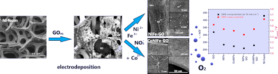
- catalytic activity of the catalysts with and without GO were studied. The catalysts were fabricated via a two-step electrodeposition. The first step included the deposition of GO flakes, which, in the second step, were reduced during the simultaneous deposition of NiFe or CoNiFe. As a result, NiFe-GO and
- the surface of nickel foam. The chronoamperometric graph recorded during the deposition is presented in Figure 1a. Each synthesis (except that of GO) began with a fast increase of the cathodic current, which is associated with the formation of the new catalyst phase on the surface of the substrate [25
- ]. Afterwards, the current density tended to stabilize for NiFe and CoNiFe, which may be associated with the steady-state formation of the catalyst film on the metallic surface. The addition of cobalt to NiFe resulted in a lower overall current density during the synthesis process. In the case of the deposition


Plasmonic nanotechnology for photothermal applications – an evaluation
Beilstein J. Nanotechnol. 2023, 14, 380–419, doi:10.3762/bjnano.14.33


Bismuth-based nanostructured photocatalysts for the remediation of antibiotics and organic dyes
Beilstein J. Nanotechnol. 2023, 14, 291–321, doi:10.3762/bjnano.14.26

- techniques have been developed to synthesise 3-D Bi-based nanostructures with different morphologies, including solvothermal/hydrothermal and sol–gel processes, mechanical exfoliation, solid-state reactions, chemical vapour deposition, and microwave-assisted techniques [106]. These 3-D photocatalysts have
- between 1-D CdS and 0-D Bi components were developed. The bandgap values were altered, and the absorption in the visible-to-infrared range was enhanced after the deposition of Bi quantum dots on CdS. To degrade the antibiotic tetracycline, a Bi/CdS heterostructure photocatalyst was used. The optimised


Biocatalytic synthesis and ordered self-assembly of silica nanoparticles via a silica-binding peptide
Beilstein J. Nanotechnol. 2023, 14, 280–290, doi:10.3762/bjnano.14.25

- revealed a hexagonal close-packed structure (insets in Figure 5a,c). In fact, the tendency of the particles formed with NH3 + 1 mM SiBP to assemble into ordered structures was visible on samples not prepared by vertical deposition but simply by dripping on a surface and vacuum drying (Figure 3d). The
- Table 2 with a final volume of 10 mL. The particles were assembled by a vertical deposition method. For SEM analysis, the particles were assembled on regular microscope cover slides. For UV–vis spectroscopy analysis, the particles were assembled on quartz slides. One end of the slide was attached to a
- ). All SEM analyses were performed using a SU5000 SEM (Hitachi, Japan) at 10 kV accelerating voltage. UV–vis absorbance spectroscopy The particles were assembled on quartz slides by vertical deposition as described before. UV–vis absorbance analysis was made using a T80+ UV–vis spectrophotometer (PG


Nanotechnology – a robust tool for fighting the challenges of drug resistance in non-small cell lung cancer
Beilstein J. Nanotechnol. 2023, 14, 240–261, doi:10.3762/bjnano.14.23

- barriers by the use of different groups of particles carrying various functional modalities. Tasciotti et al. proposed a multistage delivery system composed of stage-1 mesoporous silica particles with improved deposition in the vascular endothelium, optimized for crossing the endothelial barrier through


A novel approach to pulsed laser deposition of platinum catalyst on carbon particles for use in polymer electrolyte membrane fuel cells
Beilstein J. Nanotechnol. 2023, 14, 190–204, doi:10.3762/bjnano.14.19

- carbon substrate and the chemical synthesis of PtNPs during catalyst fabrication. Platinum was deposited on carbon particles at room temperature using a pulsed laser deposition (PLD) system equipped with an ArF excimer laser (λ = 193 nm). The uniform deposition of PtNPs on carbon supports was achieved
- thanks to a specially designed electromechanical system that mixed the carbon support particles during platinum deposition. In the studies, Vulcan XC-72R carbon black powder, a popular material used as support in the anodes and cathodes of PEMFCs, and a porous carbon material with a high degree of
- ; ORR; PEMFCs; PLD deposition; Pt catalyst; rotating ring-disk electrode (RRDE); SEM; TEM; XPS; Introduction Fuel cells, which cleanly and efficiently convert the chemical energy of hydrogen or other fuels to electrical energy, are a good alternative to dirty and wasteful combustion engines for


