Search results
Search for "valence" in Full Text gives 347 result(s) in Beilstein Journal of Nanotechnology. Showing first 200.
Absence of free carriers in silicon nanocrystals grown from phosphorus- and boron-doped silicon-rich oxide and oxynitride
Beilstein J. Nanotechnol. 2018, 9, 1501–1511, doi:10.3762/bjnano.9.141

- Si, typical dopant ionization energies are in the range of ≈50 meV. If the size of the Si crystal approaches the exciton Bohr-radius, strong quantum confinement sets in and the valence- and conduction band ground state energies shift to lower and higher energies, respectively. As a consequence, the
- situation is less critical since the conduction band offset of Si NCs and SiO2 is only about half that of the valence band offset [56]. Figure 7a shows I–t-transients of the injection-blocked MOS-capacitors (the inset depicts a schematic cross-section) measured at 0.2 MV/cm, i.e., at the onset of the J-peak


Cr(VI) remediation from aqueous environment through modified-TiO2-mediated photocatalytic reduction
Beilstein J. Nanotechnol. 2018, 9, 1448–1470, doi:10.3762/bjnano.9.137

- surface of the semiconductor. When photons with energy greater than the band gap energy of the semiconductor photocatalyst (SP) are absorbed, photogenerated electrons are excited to conduction band (CB) leaving behind holes at the valence band (VB) as per Equation 1: These photogenerated species
- cases, hole scavengers are used to facilitate the electron–hole separation process. However, application of TiO2 in photocatalysis is largely restricted mainly due to the following reasons. (i) The wide band gap of 3.2 eV causes excitation of electrons from the valence band under irradiation of UV light
- , or B narrows the band gap either by creating a mid-band gap or shifting the valence band to upper positions, resulting in a redshift. Even modification of titania with semiconductor oxides or sulfides improves the light absorption. It was evident from UV–vis DRS spectra that light absorption is


Robust midgap states in band-inverted junctions under electric and magnetic fields
Beilstein J. Nanotechnol. 2018, 9, 1405–1413, doi:10.3762/bjnano.9.133

- states are accurately described by means of a two-band model using the effective k·p approximation [18][19]. The equation governing the conduction- and valence-band envelope functions reduces to a Dirac-like equation after neglecting far-band corrections. In view of this analogy, exact solutions can be

![[Graphic 1]](/bjnano/content/inline/2190-4286-9-133-i26.svg?max-width=637&scale=1.18182) and
and ![[Graphic 2]](/bjnano/content/inline/2190-4286-9-133-i27.svg?max-width=637&scale=1.18182) band-edge profile of an abrupt band-inverted junction with aligned and same-sized gaps, l...
band-edge profile of an abrupt band-inverted junction with aligned and same-sized gaps, l...


![[Graphic 35]](/bjnano/content/inline/2190-4286-9-133-i60.svg?max-width=637&scale=1.18182) and b = 0.5 as a function of the electric field. It is important...
and b = 0.5 as a function of the electric field. It is important...

Predicting the strain-mediated topological phase transition in 3D cubic ThTaN3
Beilstein J. Nanotechnol. 2018, 9, 1399–1404, doi:10.3762/bjnano.9.132

- ThTaN3 at a lower compressive strain (5%) as shown in Figure 4. The conduction band (CB) state mainly consisted of px, py and pz orbitals of the N atom, while the valence band (VB) state is comprised of the hybridization dxy, dxz, dyz orbitals of the Ta atom. When the SOC effect was incorporated, a p–d


New 2D graphene hybrid composites as an effective base element of optical nanodevices
Beilstein J. Nanotechnol. 2018, 9, 1321–1327, doi:10.3762/bjnano.9.125

- operator vector; me and e are the free-electron mass and electron charge; En(k) and Em(k) and are the sub-band energies of, respectively, valence band and conductivity band. The spin degeneracy is already taken into account in the above equations by the factor 2, η is a phenomenological parameter


Ag2WO4 nanorods decorated with AgI nanoparticles: Novel and efficient visible-light-driven photocatalysts for the degradation of water pollutants
Beilstein J. Nanotechnol. 2018, 9, 1308–1316, doi:10.3762/bjnano.9.123

- the CB of AgI (and more holes left behind in the valence band (VB)) could readily attack the pollutant molecules, resulting in the remarkable photocatalytic performance of AgI/Ag2WO4. Conclusion In summary, a novel heterojunction photocatalyst comprised of AgI nanoparticle-decorated Ag2WO4 nanorods


Theoretical study of strain-dependent optical absorption in a doped self-assembled InAs/InGaAs/GaAs/AlGaAs quantum dot
Beilstein J. Nanotechnol. 2018, 9, 1075–1084, doi:10.3762/bjnano.9.99

- states in valence and conduction bands, Fi = 1, while Ff depends on the energy level and doping. Normally, quantum dots are occupied by a number of electrons equal to the average number of dopants per dot [34]. This approach is reasonable for quantum dots that are far from heavily doped regions. However
- the wavefunctions of the electrons and holes are localized due to these disordered band edges, as the spatial overlap between the states determines the optical absorption spectrum. Hence, one can look at the conduction and valence band edges along arbitrary lines passing through the quantum dot. This
- confinement increases the minimum allowed energy of electron Eelec and hole Ehole with respect to the band edges. Let Ebox = Eelec + Ehole, then the transition energy E is Due to the sign of the deformation potential and strain, the valence band edge inside the quantum dot is of a heavy hole, from Equation 4


Non-equilibrium electron transport induced by terahertz radiation in the topological and trivial phases of Hg1−xCdxTe
Beilstein J. Nanotechnol. 2018, 9, 1035–1039, doi:10.3762/bjnano.9.96

- concentrations correspond to the Fermi level position not lower than at 3 meV, 5 meV, and 7 meV above the conduction band edge for the samples with x = 0.13, 0.15, 0.17, respectively. The energy distance between the conduction band and the light-hole valence subband used in the Kane model calculations was
- band structure) in the samples with x < 0.16. Variable position edges of the conduction (Ec) band, the heavy hole valence (Ev) subband, and the light hole subband in the heterojunction are schematically shown by black solid lines. The Fermi level is shown by the dash-dot line. The topological layer


An implementation of spin–orbit coupling for band structure calculations with Gaussian basis sets: Two-dimensional topological crystals of Sb and Bi
Beilstein J. Nanotechnol. 2018, 9, 1015–1023, doi:10.3762/bjnano.9.94

- feature a band inversion. In a gedanken experiment, one can imagine tuning the SOC at will. As the SOC is increased from zero towards its nominal value, it pushes up the valence band while bringing down the conduction band of the imaginary SOC-free material. In this process, the gap closes and reopens
- , however, are usually restricted to the description of valence electrons, implicitly by assuming a minimal basis set of spd orbitals. The SOC is included by adding the matrix elements of the operator where λ is taken as an atomic parameter [8]. Although the simplicity of TB modeling is appealing, this
- for the interstitial or valence electrons, while approaching the core electrons differently. Since localized orbitals are convenient for a number of reasons, for instance for quantum transport calculations [15][16], a Kohn–Sham Hamiltonian obtained from plane-wave DFT codes may be transformed into a


Cyclodextrin inhibits zinc corrosion by destabilizing point defect formation in the oxide layer
Beilstein J. Nanotechnol. 2018, 9, 936–944, doi:10.3762/bjnano.9.86
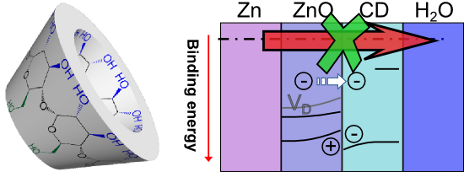
- valence band (VB) edge region. The ZnO VB region contains contributions from overlapping Zn 4s/4p, O 2p and C 2p levels [29][30]. Because of (i) the significantly bigger excitation cross-section for ZnO compared to β-CD, and (ii) the expected atomic contributions to the VB region, this region can be
- ) Zn 2p3/2, (d) Zn 3d - valence band (VB) energy region, with ZnO VB onset and ZnO VB maximum as functions of the TOA (inset). (e) Binding-energy variations for recorded spectral regions with TOA; (f) UPS HOMO onset of β-CD recorded with He II excitation. The Auger parameter α is shown as inset in (c


Effect of annealing treatments on CeO2 grown on TiN and Si substrates by atomic layer deposition
Beilstein J. Nanotechnol. 2018, 9, 890–899, doi:10.3762/bjnano.9.83

- permittivity (κ) of 23–24 [5]. In all the cases, the valence of the Ce ions is fundamental, since it determines some of the material specific ability, such as the oxygen storage. More generally, the structure of cerium oxide is essential in defining its specific capabilities [6]. At the thermodynamic
- phase or sub-stoichiometric CeO2 (CeO2−δ) can easily form. The cerium ion valence and the ceria structure can be influenced by the substrate onto which the film is grown and by thermal treatment after its deposition [7]. Also, the structural and/or the chemical composition of the substrate can influence


Facile chemical routes to mesoporous silver substrates for SERS analysis
Beilstein J. Nanotechnol. 2018, 9, 880–889, doi:10.3762/bjnano.9.82

- valence state of the silver at the surface of the mp-Ag (Figure 1f) obtained in 1:10 Ag2O/NaBH4 molar ratio. The binding energies at 368.3(2) eV and 374.2(2) eV are related to Ag 3d5/2 and Ag 3d3/2 binding energies, respectively. According to the NIST database (CAS registry No 7440-22-4) these bands


Facile synthesis of a ZnO–BiOI p–n nano-heterojunction with excellent visible-light photocatalytic activity
Beilstein J. Nanotechnol. 2018, 9, 789–800, doi:10.3762/bjnano.9.72

- out for the chemical composition and valence state analysis of various species. The foreign impurity C at 284.6 eV is used to calibrate peak positions in all the XPS results. High-resolution narrow-scan spectra of O, Bi, Zn and I are also conducted for the study of surface chemical state in detail
- -resolution scan of Bi 4f is displayed in Figure 4b. Both pure BiOI and the nanocomposite sample consist of a doublet which can be well-assigned to Bi 4f5/2 at 164.5 eV and Bi 4f3/2 at 159.2 eV with an energy difference of 5.3 eV [39][46], revealing that +3 is the main valence state of the Bi element in B-1
- coupling with ZnO, however, the satellite peaks appeared in the B-4 sample, demonstrating the chemistry state of I is changed. This probably resulted from the partial substitution of I for oxidic sites in the ZnO framework [49]. The density of electronic state (DOS) of the valence band was also


A review of carbon-based and non-carbon-based catalyst supports for the selective catalytic reduction of nitric oxide
Beilstein J. Nanotechnol. 2018, 9, 740–761, doi:10.3762/bjnano.9.68

- air at 300 °C for 50 min) and MnOx/CNT-N3 (calcined in N2 at 300 °C for 2 h) catalysts. This is greatly associated with the CNTs reducing MnOx to a lower valence state during the calcination process. Thus, thermal treatment condition plays a vital role in obtaining the best NO removal for CNT-based
Perovskite-structured CaTiO3 coupled with g-C3N4 as a heterojunction photocatalyst for organic pollutant degradation
Beilstein J. Nanotechnol. 2018, 9, 671–685, doi:10.3762/bjnano.9.62

- a distinct absorption edge in the visible region corresponding to the band gap of 2.75 eV resulting from the transfer of electrons from the valence band to the conduction band [50]. The absorption edge for CT nanoflakes lies in the UV region exhibiting a band gap of 3.45 eV. The DRS profile of CTCN
- percentage of RhB upon irradiation under different light sources. It can be seen from Figure 8d that in the presence of UV light irradiation, bare g-C3N4 degrades ≈50% of the RhB dye. This degradation is obvious because high-energy UV light can also cause excitation of electrons from the valence band to the
- responsible for the separation and migration of photogenerated charges. The appropriate band positions of the semiconductor materials produce space charge accumulation/depletion at the interfaces, which helps in the effective separation of photogenerated charge carriers [59]. In this regard, the valence band


Mechanistic insights into plasmonic photocatalysts in utilizing visible light
Beilstein J. Nanotechnol. 2018, 9, 628–648, doi:10.3762/bjnano.9.59

- semiconductor through the LSPR decay effect as illustrated in Figure 4 and Figure 5 [30], leaving behind positively charged holes at the valence band or their transfer to the counter electrode preventing recombination [16][31][32][33][34][35]. Figure 4a demonstrates the excited electron mobility from the
- which has a distinctive electronic configuration structure (filled valence band and an empty conduction band). When exposed to direct sunlight irradiation, the UV light breaks the band gap energy of TiO2 (3.2 eV) and then activates the electrons in the valence band. Thus, activated electrons move to the
- during the photocatalysis react with DMPO to convert stable DMPO–OH radicals and are detected by ESR spectroscopy. There is a high probability that the valence-band holes might alternatively oxidize the spin-trapping reagents before the formation of •OH radicals. Figure 16 shows a three-step process for


Green synthesis of fluorescent carbon dots from spices for in vitro imaging and tumour cell growth inhibition
Beilstein J. Nanotechnol. 2018, 9, 530–544, doi:10.3762/bjnano.9.51

- attributed to surface state emission, intrinsic band emission, triple ground state emission, dipole emission involving electron–phonon coupling, transition from surface electrons to valence holes, self-trapped excitons and to the presence of small organic molecules. Moreover, the characteristic excitation


Influence of the preparation method on the photocatalytic activity of Nd-modified TiO2
Beilstein J. Nanotechnol. 2018, 9, 447–459, doi:10.3762/bjnano.9.43

- are shown in Figure 3. The optical absorption of TiO2 in the UV region below 400 nm can be mainly attributed to the charge transfer, related to electron excitation from the valence band to the conduction band (band-to-band transition, O2p→Ti3d) [30]. Modification of TiO2 with neodymium significantly
- energy level in the band gap and charge transfer between the TiO2 valence band and Nd3+ ion levels [36]. Furthermore, there are four absorption bands in the vis region typical for neodymium located at 520, 585, 745 and 805 nm. They correspond to transitions from the 4I9/2 ground state to the excited


Facile synthesis of ZnFe2O4 photocatalysts for decolourization of organic dyes under solar irradiation
Beilstein J. Nanotechnol. 2018, 9, 436–446, doi:10.3762/bjnano.9.42

- material is an n-type semiconductor and the flat-band potential (Efb) was calculated to be −0.69 eV (vs Ag/AgCl) or −0.09 eV (vs RHE). From UV–vis DRS measurements, the band gap of was found to be 1.81 V. So, the valence band position of ZFO is calculated as +1.72 eV (vs RHE). By considering the calculated


Sugarcane juice derived carbon dot–graphitic carbon nitride composites for bisphenol A degradation under sunlight irradiation
Beilstein J. Nanotechnol. 2018, 9, 353–363, doi:10.3762/bjnano.9.35

- because the addition of dimethylsulfoxide (DMSO) and isopropyl alchohol (IPA) did not exert a significant effect on the degradation rate of BPA. Based on the above results, a degradation mechanism is proposed in Figure 6. The edge potential of the conduction band (CB) and the valence band (VB) of a


Review: Electrostatically actuated nanobeam-based nanoelectromechanical switches – materials solutions and operational conditions
Beilstein J. Nanotechnol. 2018, 9, 271–300, doi:10.3762/bjnano.9.29

- carry the risk of switch failure at higher operation voltages. In NEM switches with metal–semiconductor contacts, the type of the contact is determined by the mutual arrangement of the Fermi level of the metal and the valence and conduction bands of the semiconductor. The contact has a Schottky barrier
- if the Fermi level of the metal falls in between the valence and conduction bands of the semiconductor. The type of the contact (ohmic or Schottky) between two semiconductors is determined by the Fermi energies of contacting materials. The presence of a nonconductive oxide layer between the


Atomic layer deposition and properties of ZrO2/Fe2O3 thin films
Beilstein J. Nanotechnol. 2018, 9, 119–128, doi:10.3762/bjnano.9.14

- iron and zirconium oxides, the amount of defects (in particular oxygen vacancies) is increased due to the substitutive exchange between metal ions of different valence, resulting in an increase also in the leakage currents. Pure ZrO2 exhibited the lowest leakage current (Figure 7) and did not show any


Review on optofluidic microreactors for artificial photosynthesis
Beilstein J. Nanotechnol. 2018, 9, 30–41, doi:10.3762/bjnano.9.5

- energy could be offered by external light. In principle, a semiconductor photocatalyst (e.g., TiO2, C3N4) absorbs the appropriate photon (hν ≥ E0, where E0 is the bandgap of the semiconductor photocatalyst) to excite an electron in the conduction band, leaving a hole in the valence band. The electron


Facile synthesis of silver/silver thiocyanate (Ag@AgSCN) plasmonic nanostructures with enhanced photocatalytic performance
Beilstein J. Nanotechnol. 2017, 8, 2781–2789, doi:10.3762/bjnano.8.277

- absorption of Ag@AgSCN in both the UV and visible region, which is beneficial for application as a visible-light catalyst. The bandgap of AgSCN can be determined according to the Kubelka–Munk equation, which is estimated as 3.4 eV for sample M0 (Figure 2b), and the valence band value of 1.12 eV is obtained
- the reduction of AgSCN, and enhance the stability of Ag@AgSCN. The degradation mechanism suggested that electrons of Ag@AgSCN were prompted to the conduction band and holes were left in the valence band of AgSCN under irradiation (Figure 6a). The electrons were rapidly trapped by Ag nanoparticles


CdSe nanorod/TiO2 nanoparticle heterojunctions with enhanced solar- and visible-light photocatalytic activity
Beilstein J. Nanotechnol. 2017, 8, 2741–2752, doi:10.3762/bjnano.8.273

- . Photodegradation mechanism Under simulated solar light irradiation, electron (e−)/hole (h+) pairs are generated both in CdSe NRs and TiO2 nanoparticles. The holes in the valence band (VB) of TiO2 are transferred to the VB of CdSe NRs while electrons are transferred from the conduction band (CB) of CdSe NRs to the


