Search results
Search for "sensors" in Full Text gives 540 result(s) in Beilstein Journal of Nanotechnology. Showing first 200.
A silver-nanoparticle/cellulose-nanofiber composite as a highly effective substrate for surface-enhanced Raman spectroscopy
Beilstein J. Nanotechnol. 2019, 10, 1270–1279, doi:10.3762/bjnano.10.126

- nanoarchitectures developed so far have prominent application potentials in the areas of sensors and devices [26][27][28][29][30], catalysts [17][31][32], energy materials [16][32][33], as well as bio-oriented applications [34][35][36][37][38][39][40][41][42]. In the current work, a functional nanoarchitecture


Imaging the surface potential at the steps on the rutile TiO2(110) surface by Kelvin probe force microscopy
Beilstein J. Nanotechnol. 2019, 10, 1228–1236, doi:10.3762/bjnano.10.122

- steps in the catalytic reaction. Keywords: catalyst; Kelvin probe force microscopy; Smoluchowski effect; step; titanium dioxide; Introduction Titanium dioxide (TiO2) has attracted considerable interest for its promising applications as a photocatalyst and as catalyst support, as well as in gas sensors

![[Graphic 16]](/bjnano/content/inline/2190-4286-10-122-i16.svg?max-width=637&scale=1.18182) and
and ![[Graphic 17]](/bjnano/content/inline/2190-4286-10-122-i17.svg?max-width=637&scale=1.18182) .
.


![[Graphic 38]](/bjnano/content/inline/2190-4286-10-122-i38.svg?max-width=637&scale=1.18182) and
and ![[Graphic 39]](/bjnano/content/inline/2190-4286-10-122-i39.svg?max-width=637&scale=1.18182) steps. (a) Topographic image...
steps. (a) Topographic image...


![[Graphic 72]](/bjnano/content/inline/2190-4286-10-122-i72.svg?max-width=637&scale=1.18182) , b)
, b) ![[Graphic 73]](/bjnano/content/inline/2190-4286-10-122-i73.svg?max-width=637&scale=1.18182) , c) reduced
, c) reduced ![[Graphic 74]](/bjnano/content/inline/2190-4286-10-122-i74.svg?max-width=637&scale=1.18182) , and d)
, and d) ![[Graphic 75]](/bjnano/content/inline/2190-4286-10-122-i75.svg?max-width=637&scale=1.18182) steps. B...
steps. B...
Angle-dependent structural colors in a nanoscale-grating photonic crystal fabricated by reverse nanoimprint technology
Beilstein J. Nanotechnol. 2019, 10, 1211–1216, doi:10.3762/bjnano.10.120

- attracted great interest because of a possible application in visual sensors. The appearance of a photonic crystal is mainly influenced by the optical properties, structural parameters and the observation angle. In this work, an angle-sensitive photonic crystal with nanoscale gratings was fabricated through
- ; Introduction Photonic crystals have been extensively investigated in recent years because of their potential application in visual sensors [1]. Much attention has been paid to photonic crystals the reflection wavelength of which changes with the observation angle [2]. The photonic crystals can exhibit
- for applications of visual sensors. Experimental A polycarbonate (PC) master mould with period of 750 nm and height of 170 nm was fabricated through NIL. The polydimethylsiloxane (PDMS) and cross-linker were obtained from Sylgard 184 (Dow Corning, USA). The photonic crystal film with grating patterns


Photoactive nanoarchitectures based on clays incorporating TiO2 and ZnO nanoparticles
Beilstein J. Nanotechnol. 2019, 10, 1140–1156, doi:10.3762/bjnano.10.114

- metal oxides exhibit a large exciton binding energy, large piezoelectric constants and strong photoluminescence. This is of interest not only for applications as photocatalysts but also as sensors, solar cell devices, disinfectants, and cosmetics [137][138]. As discussed above, the dispersion of the


Tailoring the stability/aggregation of one-dimensional TiO2(B)/titanate nanowires using surfactants
Beilstein J. Nanotechnol. 2019, 10, 1024–1037, doi:10.3762/bjnano.10.103

- because of their unique physicochemical properties compared to the bulk material. TNMs play an important role in various applications such as photocatalytic degradation of organic pollutants [1][2], sensors [3][4], solid oxide fuel cells [5], water purification [6][7], adsorption of radioactive and heavy


Direct growth of few-layer graphene on AlN-based resonators for high-sensitivity gravimetric biosensors
Beilstein J. Nanotechnol. 2019, 10, 975–984, doi:10.3762/bjnano.10.98

- treatment that introduces a controlled density of defects in graphene, including carboxylic groups. After that, 1-ethyl-3-(3-dimethylaminopropyl)carbodiimide hydrochloride/N-hydroxysuccinimide (EDC/NHS) chemistry is used to covalently bind streptavidin molecules to the surface of the sensors. The second
- sensors emerges as a promising platform for the bio-functionalization of industrially scalable biosensors. Conclusion AlN-based solidly mounted resonators (SMRs) operating in the shear mode were covered with graphene layers intended as functionalization platforms for gravimetric biological sensors. The
- detection of anti-IgG antibodies. Two functionalization protocols were explored. In the first one, EDC/NHS chemistry was used to covalently bind streptavidin molecules to the surface of the sensors after a low-damage O2 radical plasma treatment inducing a controlled density of defects on the graphene layer


Experimental study of an evanescent-field biosensor based on 1D photonic bandgap structures
Beilstein J. Nanotechnol. 2019, 10, 967–974, doi:10.3762/bjnano.10.97

- the interaction with the target analytes in evanescent-wave-based sensors, specifically for the case of PBG sensing structures, and thus to increase the sensitivity of the sensors. The evanescent field of this type of sensing structures has been thoroughly characterized using scanning near-field
- fabricated in a silicon-on-insulator (SOI) chip in our clean-room facilities (Figure 1). The created chip layout contains four groups of sensors, each one comprising four PBG structures where the width of the transversal elements has been swept between 80 and 140 nm (wi = 80, 100, 120 and 140 nm for each of
- , including a linear taper of five elements at the accesses, leading to a total length of only ca. 22.8 µm and a footprint of only ca. 34.2 µm2. Each PBG sensors group is excited using the same access waveguide, which is divided using multimode interference (MMI) splitters. Evanescent field characterization


In situ AFM visualization of Li–O2 battery discharge products during redox cycling in an atmospherically controlled sample cell
Beilstein J. Nanotechnol. 2019, 10, 930–940, doi:10.3762/bjnano.10.94

- electrochemical cell, which was placed on the AFM scanner base (Figure 1g). The enclosure was then sealed with the probe holder (Figure 1f). The oxygen pressure in the cell was maintained at 100–200 mbarg [33]. O2 sensors in the glove box always registered an O2 concentration in the glove box of <0.1 ppm


The systemic effect of PEG-nGO-induced oxidative stress in vivo in a rodent model
Beilstein J. Nanotechnol. 2019, 10, 901–911, doi:10.3762/bjnano.10.91

- activity of GO [17]. Moreover, GO-based sensors have been used for the detection of neonicotinoids [18], tyrosine [19], ascorbic acid, dopamine, uric acid [20], 4-nitrophenol [21], and glucose [22]. Among all biocompatible polymers, PEG has been extensively used as a GO cover. Feng et al. used PEG and PEI


Rapid, ultraviolet-induced, reversibly switchable wettability of superhydrophobic/superhydrophilic surfaces
Beilstein J. Nanotechnol. 2019, 10, 866–873, doi:10.3762/bjnano.10.87

- sensors, smart filtration and separation, and microfluidic devices [9][10][11][12]. While controlling wettability through heating is mostly limited to toxic materials, such surfaces cannot be applied in human science [13][14]. Although the application of an electric field is an efficient method to achieve


Synthesis of MnO2–CuO–Fe2O3/CNTs catalysts: low-temperature SCR activity and formation mechanism
Beilstein J. Nanotechnol. 2019, 10, 848–855, doi:10.3762/bjnano.10.85

- by N2 gas. The total flow rate was 700 mL/min equivalent to a weight hourly space velocity (WHSV) of 280 L·gcat−1·h–1. A flue-gas analyzer (Kane International Limited, KM950) equipped with the NO, NO2, SO2, and O2 sensors was used to monitor the gas concentration. All data were recorded after 30 min


Novel reversibly switchable wettability of superhydrophobic–superhydrophilic surfaces induced by charge injection and heating
Beilstein J. Nanotechnol. 2019, 10, 840–847, doi:10.3762/bjnano.10.84

- , the effects of external stimuli on surface wettability have been explored extensively. For instance, chemical valves and sensors may exhibit an excellent wettability responsiveness to external physical and chemical stimuli [1][2][3]. Stimuli can be divided into: light [4][5][6][7][8][9][10][11


The effect of translation on the binding energy for transition-metal porphyrines adsorbed on Ag(111) surface
Beilstein J. Nanotechnol. 2019, 10, 706–717, doi:10.3762/bjnano.10.70

- applications can be found in the literature, ranging from molecular sensors [3] over memory devices [4] to light-harvesting structures [5][6][7]. Among all porphyrin compounds, transition-metal porphyrins (TMPPs) are of particularly interest. Because they accommodate a transition-metal atom in the center, the


![[Graphic 1]](/bjnano/content/inline/2190-4286-10-70-i1.svg?max-width=637&scale=1.18182) , for all systems and relative molecule–surface positions. Right: symm...
, for all systems and relative molecule–surface positions. Right: symm...


![[Graphic 7]](/bjnano/content/inline/2190-4286-10-70-i7.svg?max-width=637&scale=1.18182) for selected TMPP systems (M = V, Mn, Co; red: positive values, blue: negative value...
for selected TMPP systems (M = V, Mn, Co; red: positive values, blue: negative value...
Commercial polycarbonate track-etched membranes as substrates for low-cost optical sensors
Beilstein J. Nanotechnol. 2019, 10, 677–683, doi:10.3762/bjnano.10.67

- Paula Martinez-Perez Jaime Garcia-Ruperez Nanophotonics Technology Center, Universitat Politècnica de València, Camino de Vera s/n, 46022 Valencia, Spain 10.3762/bjnano.10.67 Abstract Porous materials have become one of the best options for the development of optical sensors, since they maximize
- the interaction between the optical field and the target substances, which boosts the sensitivity. In this work, we propose the use of a readily available mesoporous material for the development of such sensors: commercial polycarbonate track-etched membranes. In order to demonstrate their utility for
- porous sensors with such easily available mesoporous material. Keywords: chemical sensor; Fabry–Pérot interferometer; optical sensor; polycarbonate; track-etched membrane; Introduction Sensors are present in our daily life in order to detect and monitor chemical, biological and physical agents of


A carrier velocity model for electrical detection of gas molecules
Beilstein J. Nanotechnol. 2019, 10, 644–653, doi:10.3762/bjnano.10.64

- Engineering, Universiti Teknologi Malaysia, 81310 Skudai, Johor, Malaysia 10.3762/bjnano.10.64 Abstract Nanomaterial-based sensors with high sensitivity, fast response and recovery time, large detection range, and high chemical stability are in immense demand for the detection of hazardous gas molecules
- . Graphene nanoribbons (GNRs) which have exceptional electrical, physical, and chemical properties can fulfil all of these requirements. The detection of gas molecules using gas sensors, particularly in medical diagnostics and safety applications, is receiving particularly high demand. GNRs exhibit
- electrical, physical, and chemical properties of graphene nanoribbons (GNRs) make them very interesting for use in the future generation of the electronic devices, such as field effect transistors (FETs), diodes, capacitors, memories, and sensors [1][2]. Compared to its counterparts, such as silicon


Hydrophilicity and carbon chain length effects on the gas sensing properties of chemoresistive, self-assembled monolayer carbon nanotube sensors
Beilstein J. Nanotechnol. 2019, 10, 565–577, doi:10.3762/bjnano.10.58

- , Belgium 10.3762/bjnano.10.58 Abstract Here we describe the development of chemoresistive sensors employing oxygen-plasma-treated, Au-decorated multiwall carbon nanotubes (MWCNTs) functionalized with self-assembled monolayers (SAMs) of thiols. For the first time, the effects of the length of the carbon
- response and selectivity. This would make the detection of polar and nonpolar gas species employing low-power gas sensors easier, even under fluctuating ambient moisture conditions. Keywords: carbon length chain; gas sensing mechanism; hydrophilicity; hydrophobicity; multiwall carbon nanotubes (MWCNTs
- ); self-assembled monolayer (SAM); thiol; Introduction Carbon nanotubes were first observed by Sumio Iijima in 1991 [1] and since then, this nanostructure has been widely used in chemoresistive gas sensors [2][3][4][5] due to the possibility to engineer its sensitivity towards chemicals present in a


Widening of the electroactivity potential range by composite formation – capacitive properties of TiO2/BiVO4/PEDOT:PSS electrodes in contact with an aqueous electrolyte
Beilstein J. Nanotechnol. 2019, 10, 483–493, doi:10.3762/bjnano.10.49

- Ti/TiO2:H/BiVO4:H electrode material could be further covered by conducting polymer prepared via electrodeposition. Beside many possible applications of conducting polymers like hole-transport material [63], electrochromic layers [64], electrochemical sensors [65] and gas sensors [66], a conducting


Biological and biomimetic surfaces: adhesion, friction and wetting phenomena
Beilstein J. Nanotechnol. 2019, 10, 481–482, doi:10.3762/bjnano.10.48

- novel flow and pressure sensors. While most of the articles represent experimental work, two are devoted to theoretical and numerical work on the adhesion of rough brush systems and the friction of functionally graded materials. The metrics mentioned above illustrate that this compilation of articles
Wearable, stable, highly sensitive hydrogel–graphene strain sensors
Beilstein J. Nanotechnol. 2019, 10, 475–480, doi:10.3762/bjnano.10.47

- hydrogel strain sensor is considered to have great potential in the field of wearable sensors. Keywords: graphene; high sensitivity; hydrogel; strain sensor; wearable sensor; Introduction Wearable, flexible sensors to monitor human body pressure, temperature, strain, and chemicals hold great potential in
- the field of bioelectronics, artificial intelligence, and soft robotics [1][2]. Among these sensors, strain sensors can translate an external applied tensile force into electrical signal, hence attracting numerous research efforts for health monitoring, biomechanics studies and artificial skin for
- soft robotics [3][4]. The current, state of the art strategy to fabricate flexible strain sensors involves the integration of a conductive film on an elastomeric polymer and the embedding of conductive materials into the polymer matrix [5][6]. However, the lack of seamless conformation to curvatures in


Temperature-dependent Raman spectroscopy and sensor applications of PtSe2 nanosheets synthesized by wet chemistry
Beilstein J. Nanotechnol. 2019, 10, 467–474, doi:10.3762/bjnano.10.46

- due to its extraordinary optical, electrical, mechanical, magnetic and chemical properties [2][3][4][5]. Like graphene and its organic analogues [6], inorganic 2D metal dichalcogenides also exhibit outstanding performance in many applications including transistors, sensors, photodetectors, solar cells
- for the Eg and A1g modes was found to be −0.014 and −0.008, respectively. A room temperature humidity sensor based on the PtSe2 nanosheets demonstrated an excellent recovery time of ≈5 s, indicating the great potential of PtSe2-based sensors for future nanoelectronics and sensor devices. PtSe2


Sub-wavelength waveguide properties of 1D and surface-functionalized SnO2 nanostructures of various morphologies
Beilstein J. Nanotechnol. 2019, 10, 379–388, doi:10.3762/bjnano.10.37

- commercial application as a gas sensor, transparent conducting electrodes, and catalyst [13][14][15]. SnO2 NSs have been used in several other areas such as sub-wavelength waveguide sensors [4], microelectronics [6], Li-ion batteries [16], and lubricants [17]. Oxygen vacancy related defects in SnO2


Electromagnetic analysis of the lasing thresholds of hybrid plasmon modes of a silver tube nanolaser with active core and active shell
Beilstein J. Nanotechnol. 2019, 10, 294–304, doi:10.3762/bjnano.10.28

- HLSP modes of a silver nanotube laser with double active region. To the best of our knowledge, although these modes have been known in the passive applications such as refractive-index sensors, they have not been studied yet from the viewpoint of lasing. Results and Discussion Lasing eigenvalue problem


![[Graphic 29]](/bjnano/content/inline/2190-4286-10-28-i46.svg?max-width=637&scale=1.18182) λ = 565.03...
λ = 565.03...

![[Graphic 36]](/bjnano/content/inline/2190-4286-10-28-i53.svg?max-width=637&scale=1.18182) ...
...


Removal of toxic heavy metals from river water samples using a porous silica surface modified with a new β-ketoenolic host
Beilstein J. Nanotechnol. 2019, 10, 262–273, doi:10.3762/bjnano.10.25

- fast uranyl species sensors with high selectivity and sensitivity [43]. Our group has also recently prepared several β-ketoenols derivatives incorporated at the surface silica as effective and stable adsorbents for selective removal of toxic metals from water [44][45][46][47][48]. In the present work


Relation between thickness, crystallite size and magnetoresistance of nanostructured La1−xSrxMnyO3±δ films for magnetic field sensors
Beilstein J. Nanotechnol. 2019, 10, 256–261, doi:10.3762/bjnano.10.24

- additional supply source of precursor solution in an exponentially decreasing manner, exhibit the highest magnetoresistance and the lowest magnetoresistance anisotropy. The possibility to use these films for the development of magnetic field sensors operating at room temperature is discussed. Keywords
- : colossal magnetoresistance; crystallites; magnetic field sensors; MOCVD growth; nanostructured films; Introduction Perovskite manganite materials are an interesting topic of research since they can be applied as sensors for measuring the magnetic field due to the colossal magnetoresistance (CMR
- ) implying the possibility to use these films for the development of B-scalar sensors operating under high magnetic fields. Conclusion In this study, the nanostructured LSMO films were grown by PI-MOCVD in two different technological ways (with and without additional source of solvent) enabling the control


Magnetic-field sensor with self-reference characteristic based on a magnetic fluid and independent plasmonic dual resonances
Beilstein J. Nanotechnol. 2019, 10, 247–255, doi:10.3762/bjnano.10.23
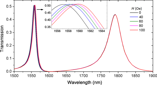
- compactness of the MDM waveguide structure. This research may open new opportunities to design nanoscale magnetic sensors with good performance. Keywords: dual resonance; magnetic fluid; magnetic sensor; plasmonic waveguide; self-reference; surface plasmon polaritons; Introduction Sensors that can detect
- the change of environmental conditions are one of the most important devices in optical communication. Optical sensors are obtained by monitoring the change of optical properties based on, e.g., thermo-optic, electro-optic, and magneto-optic effects. In the area of magnetic-field sensors, magnetic
- , such as tunable optical filters [7], optical switches [8], modulators [9] and optical sensors [10]. In particular, optical-fiber magnetic sensors have been developed by combining MFs with optical-fiber technology [11][12][13][14][15]. Optical-fiber magnetic-field sensors have the advantages of easy


