Search results
Search for "dopant" in Full Text gives 135 result(s) in Beilstein Journal of Nanotechnology.
Recent advances in green carbon dots (2015–2022): synthesis, metal ion sensing, and biological applications
Beilstein J. Nanotechnol. 2022, 13, 1068–1107, doi:10.3762/bjnano.13.93
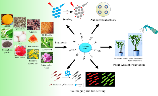
- glutathione, as a dopant for both S and N, and a green source of celery leaves to synthesize CDs. Low-cost celery leaves containing folic acid with many –COOH and –NH2 groups contribute to high QYs. The reported CDs were novel fluorescent paper sensors and showed remarkable sensitivity and selectivity in the
- synthesize hydrophilic CDs [92]. Aqueous ammonia was used as a nitrogen dopant for many natural source materials such as Hylocereus undatus (H. undatus), Chionanthus retusus (C. retusus), Phyllanthus emblica (P. emblica), and Phyllanthus acidus (P. acidus) to obtain N-CDs [93][96]. A good QY up to 31.7% was
- obtained by using EDA as N-dopant with orange juice as carbon source to give N-CDs via hydrothermal decomposition [17]. Das et al. have adopted a new strategy using κ-carrageenan as the carbon source and lemon juice as the sulfur source. Surface quaternization was performed with benzalkonium chloride to




Theoretical investigations of oxygen vacancy effects in nickel-doped zirconia from ab initio XANES spectroscopy at the oxygen K-edge
Beilstein J. Nanotechnol. 2022, 13, 975–985, doi:10.3762/bjnano.13.85
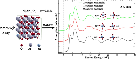
- Nanotechnologies, Institut National de Recherche en Sciences Exactes et Naturelles (IRSEN), Brazzaville, Congo 10.3762/bjnano.13.85 Abstract In this study, we present theoretical X-ray absorption near-edge structure (XANES) spectra at the K-edge of oxygen in zirconia containing Ni dopant atoms and O vacancies at
- semiconducting or insulating materials doped randomly or uniformly with magnetic impurities in the oxide matrix. A typical example are thin films of uniformly Fe-doped ZrO2 where dopant concentrations, x, from the diluted regime (i.e., x = 1–5 atom % [2]) to very high concentrations (up to x ≈ 25 atom %) have
- photoelectron spectroscopy (XPS) [26], XANES spectra [27], and synchrotron radiation measurements [4], where it was suggested that for every two dopant atoms of Fe in zirconia, one single O vacancy is created. It is, thus, expected that in similarity to the effect of Fe doping in zirconia, substitutional Ni in


Ultrafast signatures of magnetic inhomogeneity in Pd1−xFex (x ≤ 0.08) epitaxial thin films
Beilstein J. Nanotechnol. 2022, 13, 836–844, doi:10.3762/bjnano.13.74
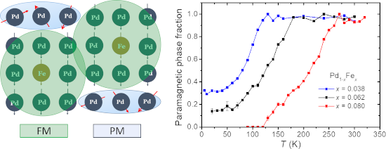
- of the iron dopant leads to a development of a temperature dependence of ΔR/R(Δt) responses, both qualitative (the appearance of new relaxation components) and quantitative (changes in their amplitudes and time constants). While two decaying exponents are sufficient to describe the relaxation of the


A chemiresistive sensor array based on polyaniline nanocomposites and machine learning classification
Beilstein J. Nanotechnol. 2022, 13, 411–423, doi:10.3762/bjnano.13.34
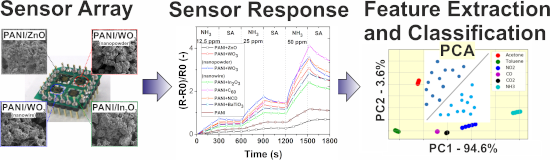
- concentration due to PANI doping and the formation of charge transfer complexes [20]. The decrease of electrical resistance is caused by the greater mobility of the dopant ions, related to the development of PANI chains. Furthermore, the swelling effect contributes to the change in resistivity [21]. Statistical




Measurement of polarization effects in dual-phase ceria-based oxygen permeation membranes using Kelvin probe force microscopy
Beilstein J. Nanotechnol. 2021, 12, 1380–1391, doi:10.3762/bjnano.12.102
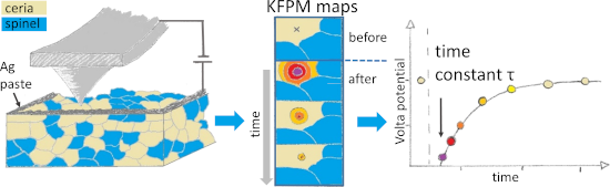
- time dependence was shown to vary with dopant concentration (e.g., abundance of oxygen vacancies in ceria) and also depends on the ratio of grain boundary/grain bulk [22][23][24][25]. Single ceria grains in a mixed ion/electron-conductive composite have so far not been addressed by AFM-based


Plasmon-enhanced photoluminescence from TiO2 and TeO2 thin films doped by Eu3+ for optoelectronic applications
Beilstein J. Nanotechnol. 2021, 12, 1271–1278, doi:10.3762/bjnano.12.94
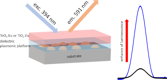
- literature [31][32]. The Eu3+ doublet is characterized by greater intensity and dominates over the Eu2+ lines. For quantitative analysis, integral intensities of europium doublets were compared. The Eu3+/Eu2+ ratio was ca. 90%:10%. Total amount of dopant in a sample was calculated to ca. 5%, on the basis of
- survey spectra. The amount of luminescent dopant in both titanium dioxide and tellurium dioxide matrixes should be sufficient to observe luminescence from the thin films. According to literature, percentage of luminescent ions in the host material should not exceed 10%. Otherwise, emission quenching may


Nickel nanoparticle-decorated reduced graphene oxide/WO3 nanocomposite – a promising candidate for gas sensing
Beilstein J. Nanotechnol. 2021, 12, 343–353, doi:10.3762/bjnano.12.28
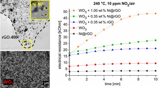
- supported on reduced graphene oxide paves the way for their application as dopant in other metal oxide gas sensors. Experimental Due to the sensitivity of the precursor substances towards moisture and oxidation, all experiments were carried out in a purified argon (grade 99.998 vol %) or nitrogen (grade


Mapping of integrated PIN diodes with a 3D architecture by scanning microwave impedance microscopy and dynamic spectroscopy
Beilstein J. Nanotechnol. 2020, 11, 1764–1775, doi:10.3762/bjnano.11.159
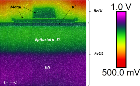
- , determined by our analytic procedure [32], as a function of VDC for both n- and p-type semiconductor materials. Using the complete metal–oxide–semiconductor equations, the Poisson–Boltzmann equation is solved for various active dopant concentration values ranging from 1015 to 1019 atoms·cm−3. In the sMIM
- fact, as expected, the amplitude of the measured local capacitance variation (∂C/∂V amplitude) increases when the doping level decreases. This behaviour allows for the localization of the P/N and I/N semiconductor junctions. As a result, the ∂C/∂V data allows for the discrimination among the dopant
- a comprehensive analysis of the overall architecture of the device for both FEOL and BEOL layers. It is important to emphasize that this result shows that, in complement to other AFM-based nanoscale electrical modes and to the local dopant density information, data regarding the BEOL layers is also


Atomic defect classification of the H–Si(100) surface through multi-mode scanning probe microscopy
Beilstein J. Nanotechnol. 2020, 11, 1346–1360, doi:10.3762/bjnano.11.119
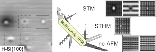
- speculated a variety of origins for this defect, including a negatively charged As dopant [58], Si-vacancy hydrogen complexes [9], and B dopants [59][60]. Crystal vacancies have previously been identified in other materials using scanning probe microscopy including Ga vacancies in GaAs [61], As vacancies in



Effect of localized helium ion irradiation on the performance of synthetic monolayer MoS2 field-effect transistors
Beilstein J. Nanotechnol. 2020, 11, 1329–1335, doi:10.3762/bjnano.11.117
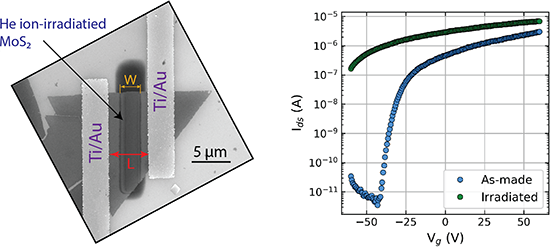
- significant n-dopant densities and suppressing the unwanted crystal structure amorphization which results from high irradiation doses. At high IR values (red group), we observe the emergence of a weak ambipolar response in our transfer curves. At these ratios, the device starts to enter a regime where more


Hybridization vs decoupling: influence of an h-BN interlayer on the physical properties of a lander-type molecule on Ni(111)
Beilstein J. Nanotechnol. 2020, 11, 1168–1177, doi:10.3762/bjnano.11.101
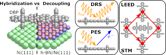
- -BN on Ni(111) exhibits an atomically flat morphology [18][19]. DBP is a promising molecule in the field of organic electronics, for example, as an electron donor [20][21][22][23] or acceptor [24] in organic photovoltaic applications, and as a dopant in organic light emitting diodes [25]. For our


Hexagonal boron nitride: a review of the emerging material platform for single-photon sources and the spin–photon interface
Beilstein J. Nanotechnol. 2020, 11, 740–769, doi:10.3762/bjnano.11.61
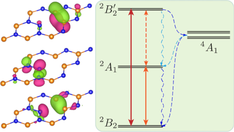
- /compatibility of the active quantum source and the device in use, and they have limitations in terms of scalability. The type of point defects that should be addressed is also a key element and is generally substitutional dopants, native vacancies, and dopant-vacancy complexes. The space of possible defects is




Structural optical and electrical properties of a transparent conductive ITO/Al–Ag/ITO multilayer contact
Beilstein J. Nanotechnol. 2020, 11, 695–702, doi:10.3762/bjnano.11.57
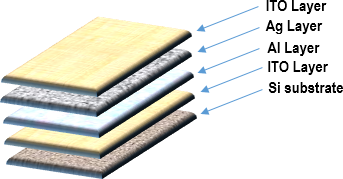
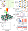
- fraction of Sn is low because it is the dopant element in ITO. The low content of Al is attributed to the very thin layer. The EDXS spectra of the films before and after annealing are shown in Figure 2. The surface morphology of the IAAI and ITO films was studied using atomic force microscopy (AFM) of an


Electrochemically derived functionalized graphene for bulk production of hydrogen peroxide
Beilstein J. Nanotechnol. 2020, 11, 432–442, doi:10.3762/bjnano.11.34
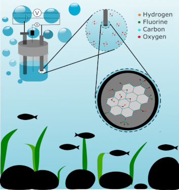
- nature of the dopant and its position in the host lattice, it has been well reported that one can engineer the electrochemical activity of nanographitic systems and the catalytic reaction pathways [31][38][39][40]. Very recently, oxidized graphitic structures were identified for their efficacy towards


Charge-transfer interactions between fullerenes and a mesoporous tetrathiafulvalene-based metal–organic framework
Beilstein J. Nanotechnol. 2019, 10, 1883–1893, doi:10.3762/bjnano.10.183
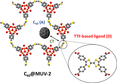
- since the fullerene is acting as a dopant introducing charge carriers within the framework. However, this enhancement in conductivity is lower in comparison to other reported systems [14][35] probably due to the low ratio between C60 and TTF (1:4) and the long distances between the TTF moieties (9.6 Å




Nanoarchitectonics meets cell surface engineering: shape recognition of human cells by halloysite-doped silica cell imprints
Beilstein J. Nanotechnol. 2019, 10, 1818–1825, doi:10.3762/bjnano.10.176
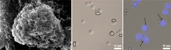
- loaded with anionic molecules (including bioactive compounds), and the loading efficiency can be significantly increased by using vacuum pumping [29]. Halloysite has already shown its potential in cells surface engineering of microbial cells [30][31]. Here we used halloysite as a dopant for artificial
- silica shells deposited on viable human HeLa cells. Halloysite nanotubes were chosen as dopant because of their biocompatibilty and rather large lumen sizes suitable for loading various drugs and even enzymes [32]. In the future, the procedure developed here can be extended to other nanotubular particles


Materials nanoarchitectonics at two-dimensional liquid interfaces
Beilstein J. Nanotechnol. 2019, 10, 1559–1587, doi:10.3762/bjnano.10.153
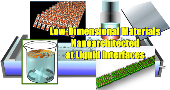
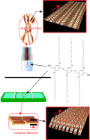
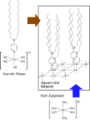
- nanoarchitectonics (controlled single atom/ion transfer) to regulate the number of dopant atoms in one-dimensional solid electrolyte nanodots (α-Ag2+δS) [127]. The nanoarchitectonic construction of one-dimensional nanowires from II–VI semiconductors was demonstrated for the use as wavelength division multiplexer as













Green fabrication of lanthanide-doped hydroxide-based phosphors: Y(OH)3:Eu3+ nanoparticles for white light generation
Beilstein J. Nanotechnol. 2019, 10, 1200–1210, doi:10.3762/bjnano.10.119
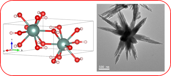
- combined with rare-earth dopants (Ce3+, Eu3+, Dy3+, etc.) [9][10][11][13]. Visible range emission from these phosphors, such as yellow, green or red, are in general the result of radiative energy transfer between partially filled 4f orbitals of dopant states together with the effective shielding of 5s and
- levels of the transition states through adjusting the dopant ion, different emission and PL intensities can be obtained [11][26][27][28]. These phosphors have been employed in various applications, including optoelectronics, field emissive displays and HDTVs, and advanced ceramics [29][30]. To date
- these requirements especially in the case of lanthanide-doped hydroxide-based phosphor fabrication, which is facile, water-based, and rapid. More specifically, acetate-based reagents of both the host and dopant are dissolved in LiOH/water solution together under room temperature. The presence of Li ions

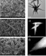


Porous N- and S-doped carbon–carbon composite electrodes by soft-templating for redox flow batteries
Beilstein J. Nanotechnol. 2019, 10, 1131–1139, doi:10.3762/bjnano.10.113
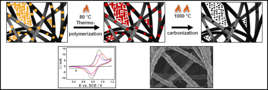
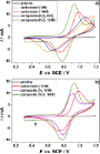
- corresponding dopant. Material synthesis To produce a suitable reference material, the pristine carbon felt was carbonized at 800 and 1000 °C under inert atmosphere (N2, 100%). The maximum temperature was held for 1 h before letting the furnace cool down. To produce composite electrodes a soft-templating



Electronic and magnetic properties of doped black phosphorene with concentration dependence
Beilstein J. Nanotechnol. 2019, 10, 993–1001, doi:10.3762/bjnano.10.100
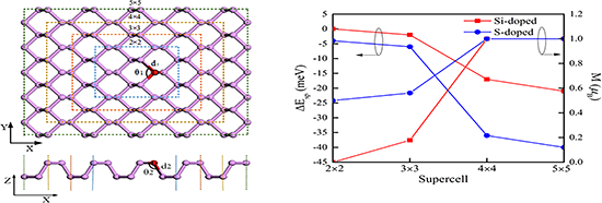
- structures of Si- and S-doped phosphorene without spin polarization always show metallic states suggesting the bandgap is insensitive to the in-plane size of the supercell and the dopant content. However, the results are fairly different once the spin polarization is taken into account. The band structures
- for the Si-doped phosphorene with 2 × 2 × 1 supercell and a dopant content of 6.25%. The magnetic moment induced by 3p orbit–spin splitting increases with the in-plane size of the supercell, and the largest magnetic moment can be found in 4 × 4 × 1 and 5 × 5 × 1 supercells. These findings offer an
- was 2 × 2 × 1 and the impurity concentration was 6.25%. They observed that all doped phosphorenes were stable, with Ca-, Ge-, and Se-doped phosphorene exhibiting metallic states. Obviously, the magnetic and electronic properties of doped phosphorene can be tuned by changing the dopant element. The


Threshold voltage decrease in a thermotropic nematic liquid crystal doped with graphene oxide flakes
Beilstein J. Nanotechnol. 2019, 10, 71–78, doi:10.3762/bjnano.10.7
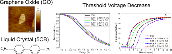
- 2 we see that the threshold voltage behavior of the 5CB-GO suspensions is reflected in the concentration dependence of K11. The small amount (0.05 wt %) of the carbon dopant leads to deterioration of properties relevant for liquid crystal applications. This is due to the increase of Uth and K11 and



Zn/F-doped tin oxide nanoparticles synthesized by laser pyrolysis: structural and optical properties
Beilstein J. Nanotechnol. 2019, 10, 9–21, doi:10.3762/bjnano.10.2
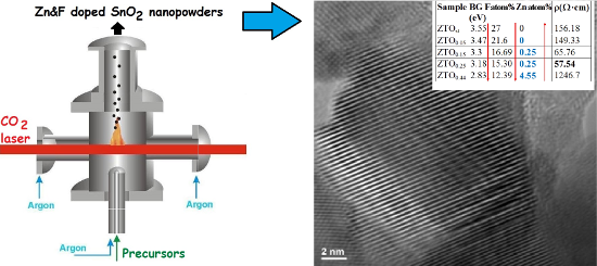
- dopant concentration). Keywords: laser pyrolysis; nanoparticles; optical bandgap; Zn/F-doped SnO2; Introduction Recently, there has been growing interest in the field of transparent conducting oxides and wide bandgap oxide nanocrystalline materials such as tin oxide (SnO2). It is generally agreed that
- case, the bandgap values decreased with increasing metal dopant content, down to 3.93 eV for 4 atom % Nd [24]. The FTO films were also successfully tested for other applications such as anticorrosive coatings on steel for fuel cell bipolar plates [25], sensors for liquefied petroleum gas [26



Charged particle single nanometre manufacturing
Beilstein J. Nanotechnol. 2018, 9, 2855–2882, doi:10.3762/bjnano.9.266
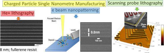
- the resist through sputtering and loss of substrate crystallinity. The situation for Ga+ ions is further complicated by the property of Ga+ as a p-type dopant of silicon. Scattering and range can be calculated using Monte Carlo simulation codes with typical results as shown in Figure 3 [30]. The
- undesirable effects such as dopant spreading associated with local temperature rise. 3.1.1 Experimental set-ups forFE-eSPL. A pattern is written by moving the scanning probe along a pre-defined path using a piezo-scanner [144]. FE-eSPL systems are typically operated in a constant-current mode [120][126], in


Variation of the photoluminescence spectrum of InAs/GaAs heterostructures grown by ion-beam deposition
Beilstein J. Nanotechnol. 2018, 9, 2794–2801, doi:10.3762/bjnano.9.261
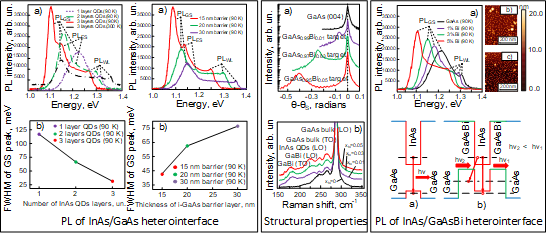
- , GaAs1−xBix films were grown on GaAs(100) substrates. The thickness of the GaAs1−xBix layers was 20 nm. The results of XRD studies of the epitaxial layer of GaAsBi are shown in Figure 3a. Bi is an isovalent dopant material for III–V compounds and replaces group-V element. Consequently, the GaAs1−xBix


Oriented zinc oxide nanorods: A novel saturable absorber for lasers in the near-infrared
Beilstein J. Nanotechnol. 2018, 9, 2730–2740, doi:10.3762/bjnano.9.255
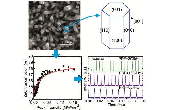
- accommodate such transition-metal ions as Mn2+ or Co2+ in the Td sites. This coordination is attractive for high ground-state transition cross-sections, so that the absorption saturation in the visible and near-IR can be observed. Moreover, the dopant ions can promote the absorption saturation due to the