Search results
Search for "electronic structure" in Full Text gives 249 result(s) in Beilstein Journal of Nanotechnology. Showing first 200.
Amorphous NixCoyP-supported TiO2 nanotube arrays as an efficient hydrogen evolution reaction electrocatalyst in acidic solution
Beilstein J. Nanotechnol. 2019, 10, 62–70, doi:10.3762/bjnano.10.6

- adding an additional metal element to these mono-metal posphides, the electronic structure and surface properties of the phosphides can be intrinsically altered that may greatly improve the catalytic performance. Compared to mono-metal phosphides, some binary metal phosphides (MgFeP, FeNiP, NiCoP, etc
- .) demonstrate a superior electrochemical performance. Because the ternary phases provide a synergistic effect, these bi-metal phosphides provide good electrical conductivity and electronic structure [15][16][17]. Among the bi-metal phosphides, Ni–Co–P catalysts have been intensively investigated. The similar


Surface plasmon resonance enhancement of photoluminescence intensity and bioimaging application of gold nanorod@CdSe/ZnS quantum dots
Beilstein J. Nanotechnol. 2019, 10, 22–31, doi:10.3762/bjnano.10.3

- fluorescence enhancement by organizing QDs on GNRs, and Anjali Kshirsagar et al. reported the electronic structure of free-standing and gold-attached passivated CdSe nanorods [24][25]. These studies covered the synthesis of GNR@CdSe/ZnS nanoparticles using different methods; however, most of these synthesis


Apparent tunneling barrier height and local work function of atomic arrays
Beilstein J. Nanotechnol. 2018, 9, 3048–3052, doi:10.3762/bjnano.9.283

- the average of the work function of the tip and the sample [21][22]. A closer look shows that factors like the image potential of the tunneling electron or the electronic structure of the electrodes complicate matters [23][24][25][26]. I still varies exponentially with z, but is replaced with an


Investigation of CVD graphene as-grown on Cu foil using simultaneous scanning tunneling/atomic force microscopy
Beilstein J. Nanotechnol. 2018, 9, 2953–2959, doi:10.3762/bjnano.9.274

- an inequivalent electronic structure in HOPG or multilayer graphene due to the presence of a carbon atom or a hollow site underneath. In this work, we report small-amplitude, simultaneous STM/AFM imaging using a metallic (tungsten) tip, of the graphene surface as-grown by chemical vapor deposition
- scanning tunneling microscopy (STM) and atomic force microscopy (AFM) by various groups [3]. The interaction of graphene with its substrate affects the STM measurements and that casts doubts on its electronic structure. Having the possibility to make simultaneous STM and AFM measurements, on the same area


Graphene-enhanced metal oxide gas sensors at room temperature: a review
Beilstein J. Nanotechnol. 2018, 9, 2832–2844, doi:10.3762/bjnano.9.264

- for semiconductor gas sensors [6]. Graphene oxide (GO), as a derivative of graphene, is prepared via the oxidation of graphene. Epoxy groups, hydroxy groups and defects are produced at the surface when oxidizing graphene [7][8][9][10]. These variations will alter the electronic structure of graphene


Biomimetic surface structures in steel fabricated with femtosecond laser pulses: influence of laser rescanning on morphology and wettability
Beilstein J. Nanotechnol. 2018, 9, 2802–2812, doi:10.3762/bjnano.9.262

- Camilo Florian Baron Alexandros Mimidis Daniel Puerto Evangelos Skoulas Emmanuel Stratakis Javier Solis Jan Siegel Laser Processing Group, Instituto de Óptica, IO-CSIC, Serrano 121, 28006 Madrid, Spain Institute of Electronic Structure and Laser (IESL), Foundation for Research and Technology


Surface energy of nanoparticles – influence of particle size and structure
Beilstein J. Nanotechnol. 2018, 9, 2265–2276, doi:10.3762/bjnano.9.211

- definition of the particle size. A more realistic definition of the particle size is possible only by a detailed analysis of the electronic structure obtained from initio calculations. Except for minor variations caused by changes in the structure, only a minor dependence of the surface energy on the
- to take care of the “electron spill-out”. De Heer proposed a correction of the particle radius of approximately 0.045–0.079 nm. According to the results of a very detailed study of the electronic structure by Holec et al. [53], the value for the correction of the diameter should be in the range of an
- 0.045 nm to 0.079 nm. According to the results of a very detailed study of the electronic structure by Holec et al. [53] the value for the correction of the diameter should be in the range of an atomic diameter (≈0.288 nm). Figure 16 displays the original values of the surface energy and that after


Intrinsic ultrasmall nanoscale silicon turns n-/p-type with SiO2/Si3N4-coating
Beilstein J. Nanotechnol. 2018, 9, 2255–2264, doi:10.3762/bjnano.9.210

- ) approach. Following an explanation of the theoretical and experimental methods used, we turn to results for Si-NCs obtained from h-DFT. Here, we focus on the electronic structure of Si-NCs as a function of the embedding dielectric and its thickness of up to 3 monolayers (MLs). The latter dependence
- optimized geometries, their electronic structure was calculated again by testing and optimizing the MO-BS wavefunction ensemble with the B3LYP hybrid DF [19][20] and the Gaussian-type 6-31G(d) MO-BS which contains d-polarization functions (B3LYP/6-31G(d)) [21] to describe the strong polar nature of atomic
- electronic structure of the Si233(NH2)87(OH)81 NWire allows ΔE values to be established for NWire electronic devices with a combined SiO2-/Si3N4-coating such as an undoped self-blocking p-channel FET (Figure 7). Using the ΔE value obtained from the Si233(NH2)87(OH)81 NWire approximant and above-described UPS


Metal-free catalysis based on nitrogen-doped carbon nanomaterials: a photoelectron spectroscopy point of view
Beilstein J. Nanotechnol. 2018, 9, 2015–2031, doi:10.3762/bjnano.9.191

- ) energies. A quarter of the target was cut out for a better visualization. (b) Impact of an ion onto a carbon nanotube, a quasi-1D system. The excess energy is dissipated in only two directions, which may affect the temperature profile and give rise to additional defects. (c) The sketch of the electronic
- structure of bulk and nanoscale objects, illustrating the so-called “phonon bottleneck” phenomenon. The excitation relaxation time is enhanced when the spacing between the size-quantized energy levels ΔE is larger than the vibrational energy ħω. This mechanism is discussed for illustration purposes only


Improving the catalytic activity for hydrogen evolution of monolayered SnSe2(1−x)S2x by mechanical strain
Beilstein J. Nanotechnol. 2018, 9, 1820–1827, doi:10.3762/bjnano.9.173

- %) and tensile (14%) strain can trigger the semiconductor–metal transition in the SnSe2 monolayer. Furthermore, Scalise et al. [15] showed that the electronic structure of the MoS2 monolayer can be reversibly tuned from direct to indirect by applying strain (ca. 2%). Much research effort has been devoted
- trace amounts of Pt nanoparticles interacting with defect-rich SnS2; the results demonstrated that SnS2 may offer new perspectives regarding a utilization in HER. The catalytic activity for HER shows great dependence on the electronic structure of the catalyst. As alloying and strain can be used to tune


Electronic conduction during the formation stages of a single-molecule junction
Beilstein J. Nanotechnol. 2018, 9, 1471–1477, doi:10.3762/bjnano.9.138

- between the two conductance pathways via the molecular bridge and across the metallic one is characterized in terms of additive independent conductance pathways, quantum interference between the two pathways, and deformed electronic structure by the presence of molecules. Finally, we reveal the different
- by two main channels, each with lower conductance contribution than 1 G0. The deviation from the trivial channel distribution can stem from distorted local electronic structure at the single-atom junction due to the presence of the molecular bridge or other nearby adsorbed molecules, such that the
- distance). Alternatively, quantum interference between the molecular and the atomic pathways can generate such nontrivial channel distribution. The first option (i.e., distortion of the local electronic structure) should also lead to asymmetric widening of the 1 G0 peak in the conductance histogram towards


Robust midgap states in band-inverted junctions under electric and magnetic fields
Beilstein J. Nanotechnol. 2018, 9, 1405–1413, doi:10.3762/bjnano.9.133

- states arising in the single-junction configuration is robust against crossed electric and magnetic fields. In addition, Landau levels of electron states lying in the semiconductor bands can be tailored by the electric field. Finally, the electronic structure of band-inverted junctions when the magnetic

![[Graphic 1]](/bjnano/content/inline/2190-4286-9-133-i26.svg?max-width=637&scale=1.18182) and
and ![[Graphic 2]](/bjnano/content/inline/2190-4286-9-133-i27.svg?max-width=637&scale=1.18182) band-edge profile of an abrupt band-inverted junction with aligned and same-sized gaps, l...
band-edge profile of an abrupt band-inverted junction with aligned and same-sized gaps, l...


![[Graphic 35]](/bjnano/content/inline/2190-4286-9-133-i60.svg?max-width=637&scale=1.18182) and b = 0.5 as a function of the electric field. It is important...
and b = 0.5 as a function of the electric field. It is important...

Predicting the strain-mediated topological phase transition in 3D cubic ThTaN3
Beilstein J. Nanotechnol. 2018, 9, 1399–1404, doi:10.3762/bjnano.9.132

- external strain. All these materials possess heavy elements and the strong SOC can induce a band inversion, which is a typical mechanism for TIs [26][27]. The experimentally observed pressure-induced phase transition in ThTaN3 indicates that the electronic structure of 3D ThTaN3 is likely very sensitive to
- (Figure 1c), the band gap reduction is significantly high (0.26 eV) after the incorporation of SOC. Then we turned to study the effect of strain [37] on the electronic structure of c-PV ThTaN3 by applying a hydrostatic strain ranging from −10% (compressive strain) to +15% (tensile strain) on 3D ThTaN3. As
- great potential for application of ThTaN3 in electronics. As eluded to above, the effect of SOC on the band gap of ThTaN3 is significant. It is therefore important to further study the effect of strain on the electronic structure of ThTaN3 in the presence of SOC (Figure 3). For strain-free ThTaN3, the


Theoretical study of strain-dependent optical absorption in a doped self-assembled InAs/InGaAs/GaAs/AlGaAs quantum dot
Beilstein J. Nanotechnol. 2018, 9, 1075–1084, doi:10.3762/bjnano.9.99

- -based projection methods [14][15]. Each atom has 20 orbitals in the sp3d5s*_SO tight-binding basis. Strain and electronic structure simulations of such large systems are computationally demanding and require highly scalable computational codes. The code used for our simulations is the Nano Electronic
- expressions for the strain components in quantum wells are = (aGaAs − aInAs)/aInAs and [24], where a is the lattice constant. Electronic structure and absorption The eigenstates of the system were calculated with a Hamiltonian constructed from semi-empirical tight-binding sp3d5s*_SO basis. The Slater–Koster


An implementation of spin–orbit coupling for band structure calculations with Gaussian basis sets: Two-dimensional topological crystals of Sb and Bi
Beilstein J. Nanotechnol. 2018, 9, 1015–1023, doi:10.3762/bjnano.9.94

- insulator, and to mono- and multilayer Sb(111) (also known as antimonene), the former being a trivial semiconductor and the latter a topological semimetal featuring topologically protected surface states. Keywords: antimonene; electronic structure; Sb few-layers; spin–orbit coupling (SOC); topological
- parameters to the specific structural variations which also needs to be parametrized [10]. On the opposite side of sophistication, the electronic structure of topological materials can be evaluated through density functional theory (DFT). According to the type of basis sets, DFT codes fall into two broad
- once a standard non-relativistic or scalar relativistic DFT calculation based on localized orbitals has been performed. Methodology Gaussian basis sets The accuracy of electronic structure calculations is limited, not only by functional, but also by the basis set used to expand the wave functions. When


Cyclodextrin inhibits zinc corrosion by destabilizing point defect formation in the oxide layer
Beilstein J. Nanotechnol. 2018, 9, 936–944, doi:10.3762/bjnano.9.86
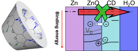
- conductive, not inhibiting further corrosion. The oxide formed on metallic Zn has noticeably different properties than crystalline bulk ZnO, due to the presence of different point defects, which have a strong effect on the electronic structure of the oxide [21][22]. ADXPS was utilized to understand defect
- levels, electronic structure, and chemical composition of the zinc surface, based on a previously established method [23][24]. Results from the β-CD/ZnO system are shown in Figure 3. Take-off-angles (TOA) close to 90° probe deeper into the volume of the sample, while low TOAs weigh surface contributions
- from impurities collected through the sample transfer. Due to the high symmetry of the Zn 2p3/2 peak, analysis of the Auger parameter α was needed to understand the electronic structure of the layer (Figure 3c). Figure 3d shows the Zn 3d region, including an inset with the depth dependence of the ZnO


Synthesis of [{AgO2CCH2OMe(PPh3)}n] and theoretical study of its use in focused electron beam induced deposition
Beilstein J. Nanotechnol. 2017, 8, 2615–2624, doi:10.3762/bjnano.8.262

- ]. Values of the hardness >3 eV and softness <0.1 eV indicate high chemical stability and hence 2 can be considered as such, indicating reliability of the approach applied. This nicely corresponds with the experimentally observed properties of 2 (see above). The electronic structure of monomeric 2 is


Inelastic electron tunneling spectroscopy of difurylethene-based photochromic single-molecule junctions
Beilstein J. Nanotechnol. 2017, 8, 2606–2614, doi:10.3762/bjnano.8.261

- Konstanz, Germany Department of Chemistry, University of Konstanz, 78457 Konstanz, Germany Okinawa Institute of Science and Technology Graduate University, Onna-son, Okinawa 904-0395, Japan 10.3762/bjnano.8.261 Abstract Diarylethene-derived molecules alter their electronic structure upon transformation
- particularly promising because of the negligible change of molecular length between the two isomers (i.e., open and closed forms) and the possibility for further chemical functionalization [13][14]. The isomerization upon illumination with appropriate wavelengths tunes the electronic structure of the molecules


Comprehensive investigation of the electronic excitation of W(CO)6 by photoabsorption and theoretical analysis in the energy region from 3.9 to 10.8 eV
Beilstein J. Nanotechnol. 2017, 8, 2208–2218, doi:10.3762/bjnano.8.220

- deposition (FEBID); photoabsorption; tungsten hexacarbonyl; Introduction The electronic structure of tungsten hexacarbonyl, W(CO)6, has previously been studied by using a variety of different experimental and theoretical methods, with experiments including vacuum ultraviolet experiments in the wavelength
- ]. The main features have been identified as bands I to V and their main characteristics are discussed below, with a complete overview and assignment of the electronic structure. The TDDFT calculations with SOC predict an important contribution of the triplet states for bands III and IV as discussed


Substrate and Mg doping effects in GaAs nanowires
Beilstein J. Nanotechnol. 2017, 8, 2126–2138, doi:10.3762/bjnano.8.212

- the GaAs nanowires on their electronic structure; ii) a considerable reduction of the density of vertical nanowires, which is almost null for growth on Si(111); iii) the occurrence of a higher WZ phase fraction, in particular for growth on Si(111); iv) an increase of the activation energy to release
- measurements showed a lower influence of the polytypic structure of the nanowires on their electronic structure. The involvement of Mg in one of the radiative transitions observed for growth on the Si(111) substrate is suggested. Keywords: electronic structure; field effect transistors; GaAs nanowires
- in the nanowires. The highest mobility was obtained for the highest free hole concentration, suggesting that, in our case, the increase of free holes in the valence band progressively blurs the contribution of the polytypic nature of the nanowires on the electronic structure [61]. The obtained PL


Electronic structure, transport, and collective effects in molecular layered systems
Beilstein J. Nanotechnol. 2017, 8, 2094–2105, doi:10.3762/bjnano.8.209

- describe the essential theoretical tools to obtain the parameters needed for the master equation from DFT results. Finally, an interacting molecular monolayer is considered within a master-equation approach. Keywords: electron correlation; electronic structure; quantum transport; spin transport
- molecules, the hybrid dimer states close to the Fermi level in the the picene/F4TCNQ compound excite a very asymmetric I–V curve with a pronounced diode-like forward/reverse current behavior. Additinally the effect of an applied gate voltage is greatly enhanced [13]. The electronic structure of free
- the microscopic details of the interface. The question arises of how the substrate interactions change the electronic structure of the molecular material and whether favorable properties for envisaged applications can be realized. Another important aspect for transport and potential applications are


![[Graphic 29]](/bjnano/content/inline/2190-4286-8-209-i41.png?max-width=637&scale=1.18182) between the occupations nA and nB of the two checkerboard sublattices for a) asy...
between the occupations nA and nB of the two checkerboard sublattices for a) asy...

![[Graphic 30]](/bjnano/content/inline/2190-4286-8-209-i42.png?max-width=637&scale=1.18182) per site for a) asymmetric tunneling, Γtop/Γbottom = 0.5, and b) symmetric tunneli...
per site for a) asymmetric tunneling, Γtop/Γbottom = 0.5, and b) symmetric tunneli...
Adsorbate-driven cooling of carbene-based molecular junctions
Beilstein J. Nanotechnol. 2017, 8, 2060–2068, doi:10.3762/bjnano.8.206

- that the charge rearrangement resulting from the adsorbate gates the carbene electronic structure and reduces the density of carbene states near the Fermi level as a function of bias. These effects result in the cooling of carbene modes at all voltages compared to the “clean” carbene-based junction. We
- a first-principles, self-consistent description of the junction out of equilibrium based on density functional theory (DFT) and non-equilibrium Green’s functions (NEGF). We show how the change in the electronic structure of the junction induced by the presence of the adsorbate promotes the cooling
- gating from that of the reduction of carbene DOS near the Fermi level due to the adsorbate. The current-induced heating of adsorbate modes reveals the important role of molecule–adsorbate through-space tunneling. By setting the adsorbate electronic structure elements to zero in the calculations we could


![[Graphic 14]](/bjnano/content/inline/2190-4286-8-206-i21.png?max-width=637&scale=1.18182) = 176 meV as a function of applied bias for the C and CA junctions, a...
= 176 meV as a function of applied bias for the C and CA junctions, a...

Identifying the nature of surface chemical modification for directed self-assembly of block copolymers
Beilstein J. Nanotechnol. 2017, 8, 1972–1981, doi:10.3762/bjnano.8.198

- the block copolymers. We have chosen hard X-ray high kinetic energy photoelectron spectroscopy as an exploration technique because it provides information on the electronic structure of buried interfaces. The outcome of the characterization sheds light onto key aspects of directed self-assembly
- photoelectron spectroscopy (HAXPES) [14]. Photoemission is a well-known technique which provides information on the electronic structure of surfaces. Its high surface sensitivity arises from the small mean free path of the outcoming photoelectrons in solid matter. Using conventional excitation sources, kinetic


Structural model of silicene-like nanoribbons on a Pb-reconstructed Si(111) surface
Beilstein J. Nanotechnol. 2017, 8, 1836–1843, doi:10.3762/bjnano.8.185

- obtained electronic structure data of the Si NRs/Si(111) system described above, scanning tunneling microscopy simulations were performed by using the Tersoff–Hamann approach [52]. Results and Discussion Typical Si nanoribbons are several nanometers long and run in one of three high-symmetry directions of

![[Graphic 9]](/bjnano/content/inline/2190-4286-8-185-i11.png?max-width=637&scale=1.18182) surface. (b) Line profile...
surface. (b) Line profile...


(Metallo)porphyrins for potential materials science applications
Beilstein J. Nanotechnol. 2017, 8, 1786–1800, doi:10.3762/bjnano.8.180

- (111). Manipulation of the electronic structure of H2TPP(OH)4 on Au(111) [45]: Molecules with two possible states, e.g., of conductivity, can be used as single-molecule switches. This functionality could be applied in nano-scaled molecular-based memory devices or logic gates [64], However, one must be
- from [44], copyright 2014 Elsevier. (a–e) Manipulation of the electronic structure by applying a voltage pulse with the STM tip at the position marked with a white circle. Converted molecules are marked with green (1→2) or blue (2→1) rectangles. (a–c) 1→2→1 conversion with 2 V pulses for 3 s (feedback


