Search results
Search for passenger subjective letter native Bering Strait Alaska 20th century in Full Text gives 405 result(s) in Beilstein Journal of Nanotechnology. Showing first 200.
Mechanism of silica–lysozyme composite formation unravelled by in situ fast SAXS
Beilstein J. Nanotechnol. 2019, 10, 182–197, doi:10.3762/bjnano.10.17

- , through the internal densification of the aggregates, the molecules gradually return to their native dimensions. This result is in agreement with findings concerning the activity of lysozyme within composites with silica, showing that smaller silica NPs (as those used for our experiments) promote higher
- enzymatic activity of lysozyme, and that this, in turn, depends on the preservation of the native shape of the molecule upon composite formation [22]. Furthermore, the formation of the silica–LZM composite is dominated, from the very moment of mixing for the initial 20 s, by a rapid, 4.5-fold increase of
- of the protein molecules are considerably smaller than the native dimensions of lysozyme in any possible orientation. Hence, this suggests that initially the binding of silica NPs by lysozyme involves a severe deformation/unfolding of the protein molecules, followed in time by a relaxation and


Nanostructured liquid crystal systems and applications
Beilstein J. Nanotechnol. 2018, 9, 2644–2645, doi:10.3762/bjnano.9.245

- that generates over ten billion dollars per year. In the 21st century, the topic of energy consumption has become a topic of critical concern for the future survival of the next generations. The new energy-saving liquid crystal devices are therefore of prime importance in industry. This in turn
Au–Si plasmonic platforms: synthesis, structure and FDTD simulations
Beilstein J. Nanotechnol. 2018, 9, 2599–2608, doi:10.3762/bjnano.9.241

- eV, is close to SiO2. The second peak can be explained by presence of very thin film of native SiO2 formed on Si substrates in air. During the heating of Au films on Si at temperatures above the eutectic temperature, an intermetallic thin layer of Au–Si is formed on the contact interface. However, it


Pattern generation for direct-write three-dimensional nanoscale structures via focused electron beam induced deposition
Beilstein J. Nanotechnol. 2018, 9, 2581–2598, doi:10.3762/bjnano.9.240


Nanocellulose: Recent advances and its prospects in environmental remediation
Beilstein J. Nanotechnol. 2018, 9, 2479–2498, doi:10.3762/bjnano.9.232

- Cladophora cellulose suggests higher inertness of its cellulose which reduces its susceptibility to chemical treatments compared to most native cellulose derived from conventional land plants. The filters fabricated from Cladophora algae cellulose have been tested and proven for trapping swine influenza


Effect of electrospinning process variables on the size of polymer fibers and bead-on-string structures established with a 23 factorial design
Beilstein J. Nanotechnol. 2018, 9, 2466–2478, doi:10.3762/bjnano.9.231

- to be obtained with expected features. Keywords: bead-on-string structure; electrospinning; factorial design; polymer fiber; Introduction Since the beginning of the 21st century, the interest in electrospinning processes has been growing constantly. The reason for this is the wide range of
- by the qualitative description of the obtained fibrous mat structures [14] and thus in a subjective way. The mathematical description of the factorial design allows the problem to be solved in a more objective manner. The factorial design, a tool used in this work, can be useful for designing the


Nanoscale characterization of the temporary adhesive of the sea urchin Paracentrotus lividus
Beilstein J. Nanotechnol. 2018, 9, 2277–2286, doi:10.3762/bjnano.9.212

- , the first nanoscale characterization of sea urchin temporary adhesives was performed using atomic force microscopy (AFM). Results: The adhesive topography was similar under dry and native (seawater) conditions, which was comprised of a honeycomb-like meshwork of aggregated globular nanostructures. In
- terms of adhesion forces, higher values were obtained in dry conditions, reaching up to 50 nN. Under native conditions, lower adhesive forces were obtained (up to 500 pN) but the adhesive seemed to behave like a functional amyloid, as evidenced by the recorded characteristic sawtooth force–extension
- curves and positive thioflavin-T labelling. Conclusion: Our results confirm that like other temporary adhesives, the sea urchin adhesive footprint nanostructure consists of a meshwork of entangled globular nanostructures. Under native conditions, the adhesive footprints of the sea urchin behaved like a


Light–Matter interactions on the nanoscale
Beilstein J. Nanotechnol. 2018, 9, 2125–2127, doi:10.3762/bjnano.9.201
- Mohsen Rahmani Chennupati Jagadish Research School of Physics and Engineering, The Australian National University, Canberra, ACT 2601, Australia 10.3762/bjnano.9.201 Keywords: light-matter interactions; nano-optics; nanophotonics; plasmonics; At the beginning of the 20th century, researchers
- century. Laser processing of thin-film multilayer structures has been one of the initial research directions in photonics [2]. This technique has been employed for many applications, including but not limited to the fabrication of polycrystalline silicon (poly-Si) thin-film transistors or MEMS/NEMS
Phosphorus monolayer doping (MLD) of silicon on insulator (SOI) substrates
Beilstein J. Nanotechnol. 2018, 9, 2106–2113, doi:10.3762/bjnano.9.199

- profiling (CVP21 Profiler) was used to determine the active carrier concentrations in the samples after the doping process was completed. Ammonium hydrogen difluoride (0.1 M) was chosen as a suitable electrolyte/etchant as it can remove the native oxide layer without etching into the underlying substrate


Localized photodeposition of catalysts using nanophotonic resonances in silicon photocathodes
Beilstein J. Nanotechnol. 2018, 9, 2097–2105, doi:10.3762/bjnano.9.198

- forward power 40 W, 7 mTorr) was used for removal of the native oxide and then HBr/O2 (5 min for nanocones and 11 min for nanowires and inverted nanocones, HF forward power 30 W, 7 mTorr) was used for etching the silicon to the desired structures. Before the etching steps an oxygen cleaning step was used


Recent highlights in nanoscale and mesoscale friction
Beilstein J. Nanotechnol. 2018, 9, 1995–2014, doi:10.3762/bjnano.9.190

- result, in vacuum, friction depends heavily on the arrangement, be it crystalline or amorphous, and the chemical nature of the surface atoms of the contacting bodies. For this reason, research in the last quarter of a century has focused on the mechanisms occurring at the atomic scale, which are


A differential Hall effect measurement method with sub-nanometre resolution for active dopant concentration profiling in ultrathin doped Si1−xGex and Si layers
Beilstein J. Nanotechnol. 2018, 9, 1926–1939, doi:10.3762/bjnano.9.184

- this work will have a minimum thickness of about 6 nm, so that the quantum-confinement effect can be neglected. An additional low-dimension effect is the dielectric confinement, which has been investigated in silicon nanowires surrounded by a dielectric material (such as its native oxide) [37][38]. For
- active. A first run of six etch cycles (15 min each) was initially performed. The sample was then kept for three days in a clean room environment. Then, a second run of three etch cycles was carried out. Both runs were initiated without removing the initial native silicon dioxide. Electrical parameters
- , it must be considered that a regrowth of native oxide occurs between the last measurement of the first run and the first measurement of the second one. This regrowth reduces the SiGe thickness by about 1 nm (as measured by ellipsometry), which results in a sheet resistance increase and a decrease of


Electrical characterization of single nanometer-wide Si fins in dense arrays
Beilstein J. Nanotechnol. 2018, 9, 1863–1867, doi:10.3762/bjnano.9.178

- voltage drop V is measured between the other two electrodes. Initially, however, the native oxides present both on the semiconducting material and the Ni-coated electrodes act as highly resistive barriers and therefore prevent any electrical contact [11]. To establish the electrical contact, the μ4pp
- technique uses the so-called punch-through current, i.e., a short current pulse of magnitude Ipulse applied between two electrodes, which causes the breakdown of the native oxide barrier [12][13][14] and hence creates the conductive path required to inject Iin into the investigated material. Empirically, it
- contact size and the contact resistance for each electrode–fin contact are, respectively, indicated by dcontact and RCj (j = 1, 2,…, 8). Note that all contact resistances are initially considered to be highly resistive because the native oxides present on both the fins and electrodes prevent current flow


Cryochemical synthesis of ultrasmall, highly crystalline, nanostructured metal oxides and salts
Beilstein J. Nanotechnol. 2018, 9, 1755–1763, doi:10.3762/bjnano.9.166

- -clean materials [1]. A cryochemical approach to study the spontaneous chemical interaction of a high-temperature substance with a gas or liquid at liquid nitrogen temperature (−196 °C) or lower appeared in the second half of the 20th century [2][3][4]. The increased use of negative temperatures (4–100 K
- . The main O 1s peak from structural oxygen is located at a binding energy (BE) of ≈529.4 eV; whereas the presence of the Ni 2p3/2 peak with a BE of ≈853.8 eV clearly indicates NiO (Figure 9a). The shape of the Ni 2p peak with characteristic satellite peaks (denoted by the letter S) also corresponds to
- synthesized using the cryochemical method: main O 1s peak is associated with structural oxygen (a) and the Ni 2p peak, containing its characteristic satellite peaks denoted by the letter S is given in (b). TEM images of sub-micrometer-sized NaNO3–NaF powders containing 3 wt % (а) and 15 wt % (b) of NaF


Preparation of micro/nanopatterned gelatins crosslinked with genipin for biocompatible dental implants
Beilstein J. Nanotechnol. 2018, 9, 1735–1754, doi:10.3762/bjnano.9.165


Magnetic properties of Fe3O4 antidot arrays synthesized by AFIR: atomic layer deposition, focused ion beam and thermal reduction
Beilstein J. Nanotechnol. 2018, 9, 1728–1734, doi:10.3762/bjnano.9.164

- material, such new Fe3O4 antidot arrays are of interest for the future development of nano-scale biosensors. Experimental Figure 1 shows the outline of the AFIR process. Si(100) wafers with a native layer of SiO2 were coated with hematite (Fe2O3) in a Savannah S100 ALD reactor from Ultratech operated at
- to manufacture square and hexagonal antidot arrays of magnetic oxides among other geometries, and with variable lattice parameters. Outline of the AFIR process. Si(100) wafers with a native layer of SiO2 were coated with Fe2O3. Antidot arrays were directly etched in the continuous films of Fe2O3


Nanoscale electrochemical response of lithium-ion cathodes: a combined study using C-AFM and SIMS
Beilstein J. Nanotechnol. 2018, 9, 1623–1628, doi:10.3762/bjnano.9.154

- materials such as the local correlation between a nanoscale stimulus and the resulting dynamically evolving material response [6]. In this letter, we propose a solution to study the nanoscale characteristics of ASB materials by a combinatorial approach that uses two established analysis techniques such as


Preparation and morphology-dependent wettability of porous alumina membranes
Beilstein J. Nanotechnol. 2018, 9, 1423–1436, doi:10.3762/bjnano.9.135

- investigate only the effect of the native surface morphology on the ICA. It was shown that the contact angle depends not only on pore diameter, but also on PAM thickness. It was found that with the increase in etching time, the pore diameter and contact angle increased for both sides. It was shown that it is


Formation mechanisms of boron oxide films fabricated by large-area electron beam-induced deposition of trimethyl borate
Beilstein J. Nanotechnol. 2018, 9, 1282–1287, doi:10.3762/bjnano.9.120

- previous studies of TEOS. This knowledge is critical for optimization of precursor chemistry in other materials systems and for future modeling efforts. Experimental EBID experiments were performed on a silicon substrate (100, n-type, P-doped, native oxide surface, MTI Corporation) with TMB precursor


A novel copper precursor for electron beam induced deposition
Beilstein J. Nanotechnol. 2018, 9, 1220–1227, doi:10.3762/bjnano.9.113

- pieces with a native oxide layer and glass cover slips with an optically characterized layer of 50 nm indium tin oxide (ITO) were used. EDX measurements were carried out in a Tescan LYRA 3 dual beam microscope equipped with an EDX Quantax system of Bruker. Spectra were taking in spot mode at an


Imaging of viscoelastic soft matter with small indentation using higher eigenmodes in single-eigenmode amplitude-modulation atomic force microscopy
Beilstein J. Nanotechnol. 2018, 9, 1116–1122, doi:10.3762/bjnano.9.103

- the deformation-rate-dependence of viscoelastic materials. We encourage further research in this area, especially in liquids, where the softest (biological) samples find their native environment. Generalized Maxwell or Wiechert mechanical model diagram representing the relationship between stress and


Room-temperature single-photon emitters in titanium dioxide optical defects
Beilstein J. Nanotechnol. 2018, 9, 1085–1094, doi:10.3762/bjnano.9.100

- [16][19][20][21][62][63][64]. For defects within nanoparticles, the emission rate can be increased by encapsulation with material having a refractive index greater than that of air [65]. The issue of native defects in oxides is generally very complex. While the molecular formation and energy


Review on nanoparticles and nanostructured materials: history, sources, toxicity and regulations
Beilstein J. Nanotechnol. 2018, 9, 1050–1074, doi:10.3762/bjnano.9.98

- process to synthesize ≈5 nm diameter PbS NPs for hair dye [23]. Similarly, “Egyptian blue” was the first synthetic pigment which was prepared and used by Egyptians using a sintered mixture nanometer-sized glass and quartz around 3rd century BC [24]. Egyptian blue represents a multifaceted mixture of
- chemical methods dates back to the 14th and 13th century BC when Egyptians and Mesopotamians started making glass using metals, which can be cited as the beginning of the metallic nanoparticle era [25]. These materials may be the earliest examples of synthetic NMs in a practical application. From the late
- ]. Nevertheless, a Roman glass workpiece is the most famous example of ancient metallic NPs usage. The Lycurgus Cups are a 4th-century Roman glass cup, made of a dichroic glass that displays different colors: red when a light passes from behind, and green when a light passes from the front [28]. Recent studies


Scanning speed phenomenon in contact-resonance atomic force microscopy
Beilstein J. Nanotechnol. 2018, 9, 945–952, doi:10.3762/bjnano.9.87

- hydrophilic sample to show that hydrodynamic stiffness of an adsorbed water layer is a plausible explanation for scan speed-induced changes in the mechanical coupling of tip and sample. Theory In air, a native adsorbed layer of water exists on all surfaces. This layer, in some cases, is several nanometers


Cyclodextrin inhibits zinc corrosion by destabilizing point defect formation in the oxide layer
Beilstein J. Nanotechnol. 2018, 9, 936–944, doi:10.3762/bjnano.9.86
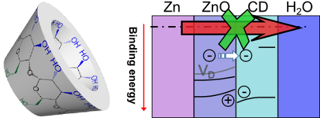
- an effect of the defect levels. The most probable defects are zinc vacancies VZn, as these have the lowest formation energy among the native point defects in ZnO [36][37]. VZn can be treated as deep acceptors, hence they should be manifested close to the top of the VB of ZnO [36][37]. A possible


