Search results
Search for "density of states" in Full Text gives 179 result(s) in Beilstein Journal of Nanotechnology.
Andreev spectrum and supercurrents in nanowire-based SNS junctions containing Majorana bound states
Beilstein J. Nanotechnol. 2018, 9, 1339–1357, doi:10.3762/bjnano.9.127

- , a highly transmissive interface between the nanowire and the superconductor is required, so that electrons can tunnel between these two systems [13][14][15][16]. This results in a superconducting nanowire, with a well-defined induced hard gap (namely, without residual quasiparticle density of states


![[Graphic 44]](/bjnano/content/inline/2190-4286-9-127-i52.svg?max-width=637&scale=1.18182) in a short SNS j...
in a short SNS j...


![[Graphic 73]](/bjnano/content/inline/2190-4286-9-127-i81.svg?max-width=637&scale=1.18182) = 0 (a,b)...
= 0 (a,b)...


![[Graphic 84]](/bjnano/content/inline/2190-4286-9-127-i92.svg?max-width=637&scale=1.18182) ), fo...
), fo...


![[Graphic 119]](/bjnano/content/inline/2190-4286-9-127-i127.svg?max-width=637&scale=1.18182) at B = 1.5Bc. Contributions to the supercurrent for (a,b) short and ...
at B = 1.5Bc. Contributions to the supercurrent for (a,b) short and ...

![[Graphic 163]](/bjnano/content/inline/2190-4286-9-127-i171.svg?max-width=637&scale=1.18182) ), in (a,b) a short and (c,d) a long junction. (a,...
), in (a,b) a short and (c,d) a long junction. (a,...

![[Graphic 175]](/bjnano/content/inline/2190-4286-9-127-i183.svg?max-width=637&scale=1.18182) ), in (a,b) a...
), in (a,b) a...

![[Graphic 186]](/bjnano/content/inline/2190-4286-9-127-i194.svg?max-width=637&scale=1.18182) ) in (a,b) a short and (c,d) a long ...
) in (a,b) a short and (c,d) a long ...
Inverse proximity effect in semiconductor Majorana nanowires
Beilstein J. Nanotechnol. 2018, 9, 1184–1193, doi:10.3762/bjnano.9.109

- resulting restrictions on the operation of Majorana-based devices. A strong paramagnetic effect for electrons entering the semiconductor together with spin–orbit coupling and van Hove singularities in the electronic density of states in the wire are responsible for the suppression of superconducting
- analogous to the one used in the phenomenological model. On top of that it gives the gap dependence on the transparency of the interface between the wire and the s-wave superconductor and chemical potential via density of states (DOS). Another important point is that the exchange of electrons between the


Thermoelectric current in topological insulator nanowires with impurities
Beilstein J. Nanotechnol. 2018, 9, 1156–1161, doi:10.3762/bjnano.9.107

- velocity vn(E) and density of states ρn(E) of a given mode n at energy E [36]. This product is a constant vn(E)ρn(E) = 1/h, irrespective of the form of εn(k), which leads to the well-known conductance quantum e2/h. For infinitely long, ballistic systems all channels are perfectly transmitted Tn = 1, so one


Cyclodextrin inhibits zinc corrosion by destabilizing point defect formation in the oxide layer
Beilstein J. Nanotechnol. 2018, 9, 936–944, doi:10.3762/bjnano.9.86
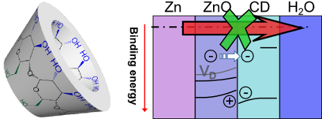
- , defect levels affect the VBonset and VBmax energy positions differently, consequently altering the density of states in the VB region. Altered density of states leads to different charge carrier densities at the interface and a decrease in potential barrier for charge dislocation.) From the magnitude of


The effect of atmospheric doping on pressure-dependent Raman scattering in supported graphene
Beilstein J. Nanotechnol. 2018, 9, 704–710, doi:10.3762/bjnano.9.65

- and copper [19] which are terminated after the transfer. Besides, this may lead to different values of the average graphene–substrate distance resulting in deviation of the density of states (DOS) from a simple Dirac cone [16] and a consequent shift of the Dirac point energy, leading to different


Revealing the interference effect of Majorana fermions in a topological Josephson junction
Beilstein J. Nanotechnol. 2018, 9, 520–529, doi:10.3762/bjnano.9.50

- the local density of states (DOS) in a topological Josephson junction. We show that the well-known 4π Josephson effect originates from the interference effect between two Majorana fermions (MFs) that are localized at the Josephson junction. In addition, the DOS for electrons (holes) shows the 4π
- interference effect of the MFs as well as the DOS by combining Andreev reflection with the electron transmission process. Keywords: density of states; fractional Josephson effect; Majorana fermion; Introduction After Kitaev reported that Majorana fermions (MFs) can appear as quasi-particle states at the ends
- topological superconductors as shown in Figure 1a. Unlike previous studies, we focus on the density of states (DOS) for both the electron part and the hole part. The essential property of the MFs is that the wave function of the electron part must be conjugated with the wave function of the hole part, which


Adsorption of iron tetraphenylporphyrin on (111) surfaces of coinage metals: a density functional theory study
Beilstein J. Nanotechnol. 2017, 8, 2484–2491, doi:10.3762/bjnano.8.248

- adsorbed FeTPP in the deckchair conformation (C2h). In the following we check the strength of different interactions involved in the adsorption of this HS FeTPP on the Au(111) surface as well as the charge transfer, work function modification and the projected density of states (PDOS) variations. In the
- contributes to electronic states around the Fermi level. We compare here the spin-resolved density of states projected (PDOS) onto the d-orbitals of Fe in the HS state before and after adsorption (with FeTPP adsorbed at the fcc site of Au(111) surface) (Figure 7). In these cases, only one orbital () is doubly
- this restriction was tested on the reference configuration (FeTPP at the hollow-fcc site of Au(111)) with a (5 × 5 × 1) Monkhorst–Pack k-point mesh. This comparison gives a difference lower than 1% for the total energy and the bond length. The difference in density of states and local electrostatic


Ester formation at the liquid–solid interface
Beilstein J. Nanotechnol. 2017, 8, 2139–2150, doi:10.3762/bjnano.8.213

- deposited solution due to enforced evaporation as well as to an increased mobility of the molecules [35]. Figure 6 shows simulated constant height mode STM images obtained from a calculated local density of states (LDOS) of the free monoester molecule. Both HOMO and LUMO show a strong intensity close to the


Substrate and Mg doping effects in GaAs nanowires
Beilstein J. Nanotechnol. 2017, 8, 2126–2138, doi:10.3762/bjnano.8.212

- term cxT3/2 accounts for the effective density of states of the band involved, and cx is a fitting parameter. Different models were tested for each component of the two samples. The best one consists of the lower number of non-radiative de-excitation channels that allows us to well describe the thermal


Electronic structure, transport, and collective effects in molecular layered systems
Beilstein J. Nanotechnol. 2017, 8, 2094–2105, doi:10.3762/bjnano.8.209

- density of states as obtained from the DFT calculations. While the electronic structure of CoPc and F16CoPc is qualitative similar after surface contact, the manganese center in the F16CoPc/MnPc yields a larger local magnetic moment and more strongly occupied metal 3d states close to the Fermi level. Both
- stack. c), d) Density of states (DOS) of the molecule-Au(111) interfaces as obtained from the calculations. The overall DOS as well as the projections onto the molecule and metal centers are shown. I–V curves calculated within the DFT-NEGF method for the sandwich structure a) CoPc/CoPc and b) F16CoPc


![[Graphic 29]](/bjnano/content/inline/2190-4286-8-209-i41.png?max-width=637&scale=1.18182) between the occupations nA and nB of the two checkerboard sublattices for a) asy...
between the occupations nA and nB of the two checkerboard sublattices for a) asy...

![[Graphic 30]](/bjnano/content/inline/2190-4286-8-209-i42.png?max-width=637&scale=1.18182) per site for a) asymmetric tunneling, Γtop/Γbottom = 0.5, and b) symmetric tunneli...
per site for a) asymmetric tunneling, Γtop/Γbottom = 0.5, and b) symmetric tunneli...
Adsorbate-driven cooling of carbene-based molecular junctions
Beilstein J. Nanotechnol. 2017, 8, 2060–2068, doi:10.3762/bjnano.8.206

- of NHC vibrational modes through i) electrostatic gating of molecular levels and ii) quenching of carbene density of states (DOS) as a function of the applied bias. We illustrate the connection between the gating of NHC states and the heating of the junction by comparing vibron populations as a
- - and right-projected DOS of the molecule while the gray curve is the density of states of the adsorbate. a) Left and right spectral functions at 0 V for a clean NHC (C, structure shown in Figure 1a,b) and with a NH2 group adsorbed on the left electrode, (CA, structure in Figure 1c,d). For the latter we


![[Graphic 14]](/bjnano/content/inline/2190-4286-8-206-i21.png?max-width=637&scale=1.18182) = 176 meV as a function of applied bias for the C and CA junctions, a...
= 176 meV as a function of applied bias for the C and CA junctions, a...

Coexistence of strongly buckled germanene phases on Al(111)
Beilstein J. Nanotechnol. 2017, 8, 1946–1951, doi:10.3762/bjnano.8.195

- bilayer germanene on Cu(111) at room temperature. Scanning tunneling spectroscopy showed a “V” shaped density of states, which was also observed by Zhang et al. [12], who synthesized germanene on MoS2 at room temperature. Al(111) was chosen as a substrate to deposit germanene by Derivaz et al. [13] with
- the motivation that it is a simple unreconstructed metal with surface density of states dominated by s-electrons. A monolayer of Ge formed at a “magic” temperature (in a range of 20 °C around 87 °C) was interpreted as a germanene layer. Well-resolved STM images showed a honeycomb arrangement of blobs
- within 0.01 eV/Å. Simulated STM images were generated from local density of states according to the Tersoff–Hamann approach [17]. The charge transfer was calculated by the Bader scheme within VASP. (a) LEED pattern obtained at an electron energy of 55 eV from Al(111) with 0.6 ML of Ge deposited at a rate


Spin-dependent transport and functional design in organic ferromagnetic devices
Beilstein J. Nanotechnol. 2017, 8, 1919–1931, doi:10.3762/bjnano.8.192

- spin filtering is realized in this bias range. The second peak of the SP appears at about 1.8 V but the SP is reduced to about 40%. In order to understand the spin filtering effect, we have calculated the spin-resolved density of states (DOS) of π-orbitals from the Green’s function with DOSσ(E,V) = −(1
- ], copyright 2007 American Physical Society. Density of states of the OF device at a bias of 0.8 V. Here, the Fermi energy of the electrodes is taken to be EF = 1.5 eV, which for a bias voltage of V = 0.8 V leads to the indicated chemical potentials μL,R = EF ± 0.4 eV. Reproduced with permission from [31
- ], copyright 2007 American Physical Society. Density of states of (a) Co and (b) the OF poly-BIPO. The molecular length is 20 sites. (c) Schematic of the magnetization configurations C1, C2, C3, and C4 in the ferromagnet/OF/ferromagnet device. Reproduced with permission from [32], copyright 2014 AIP Publishing


Structural model of silicene-like nanoribbons on a Pb-reconstructed Si(111) surface
Beilstein J. Nanotechnol. 2017, 8, 1836–1843, doi:10.3762/bjnano.8.185

- values of Φ then Pb areas, in full agreement with the experimental results. To shed light on electronic properties, we provide a comparison of the measured dI/dV characteristics and calculated density of states (DOS) in Figure 5. Again, the theoretical results reproduce well the experimental data. The
- density of states of Si NR system in the absence (red line) and in the presence of Pb atoms (black line). Note that the system is metallic. Relative surface energies γNR(Si) and BP–BP distance dBP of structural models of Si NRs on the Si(111) surface. γNR(Si), defined by Equation 1, is measured with

![[Graphic 9]](/bjnano/content/inline/2190-4286-8-185-i11.png?max-width=637&scale=1.18182) surface. (b) Line profile...
surface. (b) Line profile...


Fluorination of vertically aligned carbon nanotubes: from CF4 plasma chemistry to surface functionalization
Beilstein J. Nanotechnol. 2017, 8, 1723–1733, doi:10.3762/bjnano.8.173

- energy range extending from 28 eV to the Fermi level (corresponding to 0 eV), the projected density of states of the pristine sample is dominated by C–C π state appearing around 3 eV, together with the C–C σ state placed around 8 eV and the σ–π hybridized states that extend from around 10 eV towards
- intensity of the peak around 10 eV and at 15 eV to the F 2p-like states and to the F–C 2s bonding orbitals, respectively [19][27]. The fluorine grafting drastically reduces also the density of states just below the Fermi level. A close view of this region is illustrated in the frame, where the dotted red
- about 1.3 eV when the fluorine content at the sample surface is 8 atom %, indicating the possibility to tune the threshold energy. As a consequence of the fluorine desorption, the fluorine-related states are less dominant, in fact, the relative intensity of the density of states nearby the Fermi level


Transport characteristics of a silicene nanoribbon on Ag(110)
Beilstein J. Nanotechnol. 2017, 8, 1699–1704, doi:10.3762/bjnano.8.170

- SiNR nanojunctions. Since the dI/dV spectrum essentially reflects the electronic density of states (DOS), we interpret the peak by comparing the dI/dV spectrum with the DOS spectra calculated for freestanding SiNR. The DFT studies have demonstrated that the geometric and electronic structures of SiNR


Effect of the fluorination technique on the surface-fluorination patterning of double-walled carbon nanotubes
Beilstein J. Nanotechnol. 2017, 8, 1688–1698, doi:10.3762/bjnano.8.169

- [29]. A spectrum arises as a result of core-level electrons being excited into partially filled and empty states, thus providing information about the unoccupied density of states of the X-ray absorbing elements. We consider the F K-edge spectra because they showed a considerable variation of the pre


Charge transfer from and to manganese phthalocyanine: bulk materials and interfaces
Beilstein J. Nanotechnol. 2017, 8, 1601–1615, doi:10.3762/bjnano.8.160

- . PES [37][38][39] is based on the photoelectric effect and provides insight into the valence-band electronic density of states as well as the binding energy and line shape of core levels, which give information about the composition of the sample and the chemical state (e.g., valency) of the atoms or
- ions. In IPES [19][40][41][42], the unoccupied density of states is probed. EELS [43][44][45] can also be called inelastic electron scattering and measures the electronic excitations either in the valence-band region, or from core levels into unoccupied states, whereas momentum-dependent studies are
- possible [43][45][46]. The EELS cross section is proportional to Im(−1/ε) (ε is the dielectric function). In this way, one can investigate valence-band excitations (cf. optical methods) and the element-projected unoccupied density of states. Also, access to orbital selective occupations and the magnetic


Adsorption and electronic properties of pentacene on thin dielectric decoupling layers
Beilstein J. Nanotechnol. 2017, 8, 1388–1395, doi:10.3762/bjnano.8.140

- well-defined increases in the local density of states are observed close to the Fermi level [3][4]. Tunneling through these states of pentacene results in a temporary charging of the molecule prior to the dissipation of the charge into the substrate [5]. The peaks observed in STS on pentacene are


Ultrasmall magnetic field-effect and sign reversal in transistors based on donor/acceptor systems
Beilstein J. Nanotechnol. 2017, 8, 1104–1114, doi:10.3762/bjnano.8.112

- ][36][37][38]. Doping of amorphous organic films results in a broadening of the density of states and, thus, is increasing the energetic disorder [39][40]. Therefore, the high density of intrinsic charges in Spiro-TTB/HAT-CN compositions as well as the broadened density of states leads to an increased


Stable Au–C bonds to the substrate for fullerene-based nanostructures
Beilstein J. Nanotechnol. 2017, 8, 1073–1079, doi:10.3762/bjnano.8.109

- the electronic properties of the adsorbed fullerenes with vacancy defect, and compare them to those of the C60/Au(111) system. Figure 5 shows the calculated density of states (DOS) of the isolated molecule (dashed lines) and junction (solid lines) projected onto the molecular atoms. Upon adsorption


Near-field surface plasmon field enhancement induced by rippled surfaces
Beilstein J. Nanotechnol. 2017, 8, 956–967, doi:10.3762/bjnano.8.97

- is characterized by N ≈ 1 hot spots with localized length ξl whereas delocalized modes involve N >> 1 hot spots, with average length ξ >> ξl so that for localized modes χ ≈ ξl−2. Carminati et al. have shown that high values of the χ parameter correspond to large fluctuations of the local density of
- states (LDOSs) [52]. Each QNM is described by the Green’s functions, Equation 9 and Equation 12, that are closely related to the LDOSs. The LDOSs represents the weight of all normalized QNMs at a certain point of space for a certain light frequency and can be calculated by Equation 16. In Equation 16 G


Energy-level alignment at interfaces between manganese phthalocyanine and C60
Beilstein J. Nanotechnol. 2017, 8, 927–932, doi:10.3762/bjnano.8.94

- deposited first and the metal substrate (gold) varies going from MnPc to C60 with the consequence of a different Fermi-level position in the layer stack. Moreover, in previous studies [25][53] the importance of interface morphologies, molecular orientations and the resulting density of states on the energy


Advances in the fabrication of graphene transistors on flexible substrates
Beilstein J. Nanotechnol. 2017, 8, 467–474, doi:10.3762/bjnano.8.50

- in graphene FETs (Gr-FETs) even with gradually scaled (≈0.5 µm) channel lengths fabricated on a flexible polyimide substrate and adopting a back-gate configuration and Al2O3 as a gate dielectric. In addition, due to the low density of states (DOS) around the Dirac point, the carrier density of


Tunable plasmons in regular planar arrays of graphene nanoribbons with armchair and zigzag-shaped edges
Beilstein J. Nanotechnol. 2017, 8, 172–182, doi:10.3762/bjnano.8.18

- region is further scrutinized with a finer MP mesh of 2000 × 1 × 1 k-points, including up to 30 bands. The main results of our DFT computations are summarized in the plots of Figure 1, which show the different geometry, band structure and density of states (DOS) of the GNR arrays. 4ZGNR and 10ZGNR behave


![[Graphic 8]](/bjnano/content/inline/2190-4286-8-18-i16.png?max-width=637&scale=1.18182) , Equation 6) and EL function (ELOSS, Equation 8) at room temperature for the GNR arrays of Figure 1 ...
, Equation 6) and EL function (ELOSS, Equation 8) at room temperature for the GNR arrays of Figure 1 ...


