Search results
Search for "in situ" in Full Text gives 482 result(s) in Beilstein Journal of Nanotechnology. Showing first 200.
Direct AFM-based nanoscale mapping and tomography of open-circuit voltages for photovoltaics
Beilstein J. Nanotechnol. 2018, 9, 1802–1808, doi:10.3762/bjnano.9.171

- during in situ illumination reveal local to mesoscale contributions to PV performance based on the order of magnitude variations in photovoltaic properties with distinct grains, at grain boundaries, and for sub-granular planar defects. Keywords: cadmium telluride (CdTe); photo-conductive AFM (pcAFM); PV
- interconnects [4][5], and tomographic AFM of photocurrents in polycrystalline solar cells during in situ illumination [6]. Standard photo-conductive AFM (pcAFM) employs a conducting probe, which serves as a positionable top electrode, to map currents upon illumination and/or biasing. With solar cells, the short


SO2 gas adsorption on carbon nanomaterials: a comparative study
Beilstein J. Nanotechnol. 2018, 9, 1782–1792, doi:10.3762/bjnano.9.169

- adsorption [43]. By combining in situ powder X-ray diffraction and inelastic neutron scattering measurements with simulation studies, Yang et al. argued that hydroxy groups within the pore channels selectively bind SO2 by the formation of hydrogen bonds that are reinforced by weaker phenyl C–H…O=S=O


Multimodal noncontact atomic force microscopy and Kelvin probe force microscopy investigations of organolead tribromide perovskite single crystals
Beilstein J. Nanotechnol. 2018, 9, 1695–1704, doi:10.3762/bjnano.9.161

- ) at room temperature (RT) with in situ annealed Pt/Ir-coated silicon cantilevers (EFM, Nanosensors, resonance frequency in the 45–115 kHz range). Topographical imaging was performed in frequency modulation mode (FM-AFM) with negative frequency shifts of a few Hz and vibration amplitudes of a few tens
- ambient atmosphere during the cleaving process. Alternatively, one may also hypothesize that intrinsic defects are formed during the solution process crystal growth. Addressing the origin of these defects is beyond the scope of the current work, and will require development of in situ cleaving facilities


Sheet-on-belt branched TiO2(B)/rGO powders with enhanced photocatalytic activity
Beilstein J. Nanotechnol. 2018, 9, 1550–1557, doi:10.3762/bjnano.9.146

- photocatalytic activity [40]. Conclusion TiO2(B) nanosheet branches were uniformly in situ grown on TiO2/rGO nanobelt surfaces to form a unique sheet-on-belt nanostructure. Both trunks and branches were TiO2(B); however, the photoluminescence measurements suggest an enhanced charge separation of the branched


Electronic conduction during the formation stages of a single-molecule junction
Beilstein J. Nanotechnol. 2018, 9, 1471–1477, doi:10.3762/bjnano.9.138

- cryogenic vacuum conditions. Molecular junctions are prepared by sublimating vanadocene molecules (95%, Buchem, further purified in situ), from a locally heated molecular source towards the metallic junction, while repeatedly breaking and reforming the junction between the two electrodes to study molecular


Cr(VI) remediation from aqueous environment through modified-TiO2-mediated photocatalytic reduction
Beilstein J. Nanotechnol. 2018, 9, 1448–1470, doi:10.3762/bjnano.9.137

- photoreduction of Cr(VI) under sunlight illumination [143]. Its enhanced photoreduction capacity over TiO2 nanosheets, P25 and CD–P25 was attributed to the better charge transfer as well as higher light absorption properties of CDs. The in situ formation of H2O2 promotes the photoactivity to a great extent


Ag2WO4 nanorods decorated with AgI nanoparticles: Novel and efficient visible-light-driven photocatalysts for the degradation of water pollutants
Beilstein J. Nanotechnol. 2018, 9, 1308–1316, doi:10.3762/bjnano.9.123

- , to enhance the photocatalytic performance of Ag2WO4, AgI (possessing matched energy band levels) was chosen as a suitable component to combine with Ag2WO4, AgI/Ag2WO4 heterojunctions at different mole ratios. These heterojunctions were prepared via an in situ ion-exchange approach, utilizing Ag2WO4
- possible photocatalytic mechanism over AgI/Ag2WO4 was also elucidated in this work. Results and Discussion Preparation and characterization of catalysts Ag2WO4 nanorods decorated with AgI nanoparticles were prepared via an in situ anion-exchange method. Ag2WO4 nanorods were first synthesized by mixing
- AgNO3 and Na2WO4 aqueous solutions at room temperature [37]. Subsequently, AgI nanoparticles were readily anchored onto Ag2WO4 nanorods via an in situ anion-exchange between I− in the solution and the lattice W2O42− in Ag2WO4. The resulting catalysts were denoted as 0.1AgI/Ag2WO4, 0.2AgI/Ag2WO4, 0.3AgI


Formation mechanisms of boron oxide films fabricated by large-area electron beam-induced deposition of trimethyl borate
Beilstein J. Nanotechnol. 2018, 9, 1282–1287, doi:10.3762/bjnano.9.120

- ultrathin window, and a 10 eV per channel multi-channel analyzer. In situ optical images where captured using a Navitar Zoom 6000 Lens System and CCD Camera (Thorlabs, DCU224C). The optical images captured a region deposited at room temperature on a copper-coated silicon substrate (100 nm thick copper layer
- of the deposit fabricated at a substrate temperature of 63 °C. (b) Side-on, in situ optical image of deposit produced by the large-area EBID system. The deposit was fabricated by performing EBID using TMB precursor on a room temperature copper-coated silicon substrate for 30 min. (c) LCSM optical


Electrostatic force spectroscopy revealing the degree of reduction of individual graphene oxide sheets
Beilstein J. Nanotechnol. 2018, 9, 1146–1155, doi:10.3762/bjnano.9.106

- various methods. C 1s XPS spectra of (a, top) sample 0, (a, bottom) sample 5, and (b) samples 0–5; (c) normalized UV–vis absorption spectra of samples 0–5; in situ SPFM images of GO sheets thermally reduced at 150 °C for (d) 0 min, (e) 15 min, and (f) 75 min; (g) SPFM image of sample 1 (the in situ
- tapping AFM image is highlighted by the white rectangle); (h) tapping AFM and (i) in situ SPFM images of the mixture of sample 0 and 5; (j) tapping AFM and (k) in situ SPFM images of sample 5; cross-sectional profiles along (l) the lines in (d–f), (m) the lines in (k) and (n) the lines in (g, i). The
- numbers in the top right corners of the images (g, h, j) represent the sample numbers. The white scale bars represent 1000 nm. The z-scale bar is shown to the right of each SPM image. Characterizing the degree of reduction of GO sheets using EFM imaging and EFS: (a) tapping AFM image and in situ EFM


Magnetic characterization of cobalt nanowires and square nanorings fabricated by focused electron beam induced deposition
Beilstein J. Nanotechnol. 2018, 9, 1040–1049, doi:10.3762/bjnano.9.97

- of a square hysteresis loop with a coercive field of approximately 10 mT. L-TEM images of square nanorings revealed a horseshoe magnetic state, which could be changed to an opposite horseshoe state by reversing the magnetic field applied in situ. By increasing the external magnetic field and


Single-crystalline FeCo nanoparticle-filled carbon nanotubes: synthesis, structural characterization and magnetic properties
Beilstein J. Nanotechnol. 2018, 9, 1024–1034, doi:10.3762/bjnano.9.95

- the filling material due to the confinement of the material within the hollow tubular cavity. Chemical vapor deposition (CVD) is a technique used to fill MNPs into CNTs via in situ filling, in which metallocene precursors are used as a carbon source and MNPs [22][30][37] or hydrocarbons (such as


Cyclodextrin inhibits zinc corrosion by destabilizing point defect formation in the oxide layer
Beilstein J. Nanotechnol. 2018, 9, 936–944, doi:10.3762/bjnano.9.86
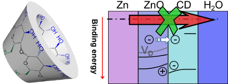
- the EIS measurements a quantitative comparison of the efficiencies is not reasonable. In situ spectroscopic ellipsometry experiments conducted both in 0.1 M KCl as well as in 0.1 M KCl with 5.3 mM β-CD show no formation of an adsorbate layer on the samples (Supporting Information File 1, Figure S6
- microscope. The samples were irradiated with an excitation wavelength of 532.1 nm/2.33 eV through a microscope objective of 100× magnification and with a numerical aperture of 0.75. In situ spectroscopic ellipsometry (SE) was performed on Zn samples polished down to a 1 μm diamond suspension. Experiments
- were performed at an angle of incidence of 70° using a Sentech Instruments SE 800 spectroscopic ellipsometer working in the wavelength range of 280–810 nm (1.5–4.4 eV). The details of the used in situ cell were described elsewhere [47][48]. Experiments were done in 0.1 M KCl, both in the presence and


Nanoscale mapping of dielectric properties based on surface adhesion force measurements
Beilstein J. Nanotechnol. 2018, 9, 900–906, doi:10.3762/bjnano.9.84

- ). So the effect of the contact potential difference between the tip and our sample was ignored in our experiments. A comparison study of dielectric property mapping by adhesion force and SPFM was also carried out. Figure 3g shows an in situ SPFM image of Figure 3c taken with an AFM tip biased at 10 V
- ambient conditions. (d) Cross-sectional profiles of the white dotted line in (a). (e) Cross sectional profiles of the blue and red dotted lines in (b) and (c), respectively. (f) The average adhesion forces of GO and RGO sheets under AFM tip biases of 0 and 10 V, respectively. (g) An in situ SPFM image of


Effect of annealing treatments on CeO2 grown on TiN and Si substrates by atomic layer deposition
Beilstein J. Nanotechnol. 2018, 9, 890–899, doi:10.3762/bjnano.9.83

- attention to the interface with the substrate. The annealing treatments have been performed in situ during the acquisition of X-Ray diffraction patterns to monitor the structural changes in the film. We find that ceria film is thermally stable up to annealing temperatures of 900 °C required for the complete
- ; in situ annealing; transmission electron microscopy; X-ray diffraction; Introduction Cerium dioxide (CeO2) has raised renewed interest in the recent years in many fields of research thanks to its properties, such as the ability to store and release oxygen, or its chemical stability [1][2]. For many
- study of the first deposition steps of CeO2 by thermal ALD upon different substrates is required to fully elucidate the mechanism of the growth and nucleation of CeO2, and possibly validate our proposed phenomenological model. A possible approach would be the study by dedicated in situ ALD growth at


Facile chemical routes to mesoporous silver substrates for SERS analysis
Beilstein J. Nanotechnol. 2018, 9, 880–889, doi:10.3762/bjnano.9.82

- )-active substrates. An analogous procedure was successfully performed for the production of mesoporous silver films by chemical reduction of oxidized silver films. The sponge-like silver blocks with high surface area and the in-situ-prepared mesoporous silver films are efficient as both analyte adsorbents


Comparative study of antibacterial properties of polystyrene films with TiOx and Cu nanoparticles fabricated using cluster beam technique
Beilstein J. Nanotechnol. 2018, 9, 861–869, doi:10.3762/bjnano.9.80

- of consumables for medicine (for example, catheters for drug delivery) [7][8]. There are different ways for the formation of polymers with metal NPs. Particles can be synthesized in situ using the organic matrix as the reaction medium or ex situ by chemical or physical means and then incorporated


A review of carbon-based and non-carbon-based catalyst supports for the selective catalytic reduction of nitric oxide
Beilstein J. Nanotechnol. 2018, 9, 740–761, doi:10.3762/bjnano.9.68

- –Ce species on CNT using an in situ (reflux) method. In this method, poly(sodium 4-styrenesulonate) (PSS) was used as surfactant during the synthesis of the catalyst in order to assist with the dispersion of CNTs in aqueous solution and to maintain its stability. From the experimental activities, it
Combined pulsed laser deposition and non-contact atomic force microscopy system for studies of insulator metal oxide thin films
Beilstein J. Nanotechnol. 2018, 9, 686–692, doi:10.3762/bjnano.9.63

- systems allow for in situ observations, from sample preparation to measurements. In order to image surface atoms of insulator metal oxides with atomic resolution, in this study, we have developed a combined system consisting of an NC-AFM and PLD operated in ultra-high vacuum (UHV) at room temperature. In
- for checking the crystal structure, orientation plane, and crystallinity of a thin film. Once a single-atomic layer step is confirmed, a new sample is prepared under the same PLD conditions and in situ NC-AFM (and also STM) measurements can then be performed in UHV. As an example, a process flow for
- magnetoresistance [61]. Figure 4 shows results of atomic-resolution measurements of anatase TiO2(001) and LaAlO3(100) using the NC-AFM. We determined the PLD conditions according to the procedure mentioned above, described in the caption of Figure 4. LEED measurements were also performed in situ after the NC-AFM


Tuning adhesion forces between functionalized gold colloidal nanoparticles and silicon AFM tips: role of ligands and capillary forces
Beilstein J. Nanotechnol. 2018, 9, 660–670, doi:10.3762/bjnano.9.61

- received. Common NPs functionalization methods can be tuned to allow improvements of the modification of NPs surface functionality by choosing the appropriate number of steps: from one step (in situ synthesis) up to several (ex situ), if necessary. The one-step method described in [49] was applied for the


Mechanistic insights into plasmonic photocatalysts in utilizing visible light
Beilstein J. Nanotechnol. 2018, 9, 628–648, doi:10.3762/bjnano.9.59

- polarized irradiation along various axes was combined with theoretical simulations based on the finite element method (FEM). In situ XAS was used to understand the electronic structural changes caused by the electromagnetic field upon the surface of plasmonic materials [108]. Designing the physical


Towards 3D crystal orientation reconstruction using automated crystal orientation mapping transmission electron microscopy (ACOM-TEM)
Beilstein J. Nanotechnol. 2018, 9, 602–607, doi:10.3762/bjnano.9.56

- ), Hermann-von-Helmholtz-Platz 1, 76344 Eggenstein-Leopoldshafen, Germany 10.3762/bjnano.9.56 Abstract To relate the internal structure of a volume (crystallite and phase boundaries) to properties (electrical, magnetic, mechanical, thermal), a full 3D reconstruction in combination with in situ testing is
- desirable. In situ testing allows the crystallographic changes in a material to be followed by tracking and comparing the individual crystals and phases. Standard transmission electron microscopy (TEM) delivers a projection image through the 3D volume of an electron-transparent TEM sample lamella. Only with
- times. The combination of in situ testing with 3D crystal orientation mapping remains a challenge in terms of stability and accuracy. Here, we outline a method to 3D reconstruct the crystal orientation from a superimposed diffraction pattern of overlapping crystals without sample tilt. Avoiding the


Anchoring Fe3O4 nanoparticles in a reduced graphene oxide aerogel matrix via polydopamine coating
Beilstein J. Nanotechnol. 2018, 9, 591–601, doi:10.3762/bjnano.9.55

- introduction into aerogel. The first method is based on the addition of iron precursors to GO water dispersion and “in situ” synthesis of iron oxide MNPs during hydrothermal hydrogel formation in autoclave. The precipitated nanoparticles are anchored to GO structure via Fe–C–O bonds or confined between GO


Electron interactions with the heteronuclear carbonyl precursor H2FeRu3(CO)13 and comparison with HFeCo3(CO)12: from fundamental gas phase and surface science studies to focused electron beam induced deposition
Beilstein J. Nanotechnol. 2018, 9, 555–579, doi:10.3762/bjnano.9.53

- such as Pt and Au by post-growth treatment and in situ injection of water for carbon removal [6][7][8][9][10][11][12][13]. These oxidative processes are suitable for precious metals, while other approaches such as annealing under vacuum [14] and hydrogen atmosphere [15][16] are suitable for metals such
- monitored in situ by X-ray photoelectron spectroscopy (XPS) and mass spectrometry. Figure 9 shows the evolution of the O 1s, Fe 2p and Ru 3d/C 1s XPS regions of a nanometer-thick film of H2FeRu3(CO)13 adsorbed onto a gold substrate at 213 K, plotted as a function of increasing electron dose. Area analysis


Engineering of oriented carbon nanotubes in composite materials
Beilstein J. Nanotechnol. 2018, 9, 415–435, doi:10.3762/bjnano.9.41

- -45639, Iran 10.3762/bjnano.9.41 Abstract The orientation and arrangement engineering of carbon nanotubes (CNTs) in composite structures is considered a challenging issue. In this regard, two groups of in situ and ex situ techniques have been developed. In the first, the arrangement is achieved during
- arrangement) are presented and discussed. Post-growth sorting of CNTs in a composite material structure As mentioned above, the methods for arranging CNTs are divided into two main categories: orientation during growth (in situ) and post-growth (ex situ). In post-growth orientation processes, the CNTs are
- initially produced using conventional methods. Then, by applying a distinct process, they are arranged for a specific purpose. Compared with in situ methods, ex situ methods do not have limitations in the production of CNTs, such as restriction on the substrate type and processing temperature, and also the


Electron interaction with copper(II) carboxylate compounds
Beilstein J. Nanotechnol. 2018, 9, 384–398, doi:10.3762/bjnano.9.38

- . Materials Copper(II) carboxylate compounds with tert-butylamine of the general formula [Cu2(t-BuNH2)2(µ-O2CR)4], where R = CnF2n+1, n = 1–6, were obtained in the reaction of copper(II) perfluorinated carboxylates with tert-butylamine, which was in situ generated from tert-butyl isocyanate [34]: The


