


Search results
Search for "semiconductors" in Full Text gives 357 result(s) in Beilstein Journal of Nanotechnology. Showing first 200.
Near-infrared light harvesting of upconverting NaYF4:Yb3+/Er3+-based amorphous silicon solar cells investigated by an optical filter
Beilstein J. Nanotechnol. 2018, 9, 2788–2793, doi:10.3762/bjnano.9.260
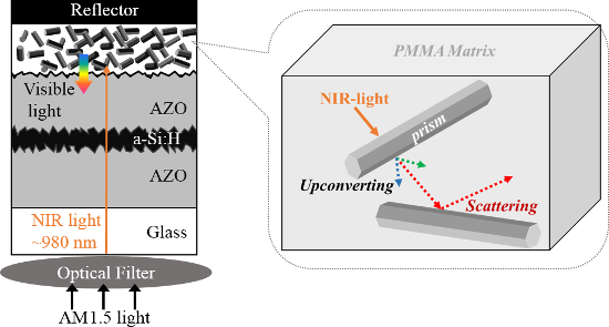
- above-bandgap visible light. The photons generated during upconversion are then absorbed by photoactive semiconductors to generate electron–hole pairs. This means that UC can broaden the absorption spectrum and enhance the photoelectric conversion efficiency of solar cells. Based on a detailed balance


Contactless photomagnetoelectric investigations of 2D semiconductors
Beilstein J. Nanotechnol. 2018, 9, 2741–2749, doi:10.3762/bjnano.9.256
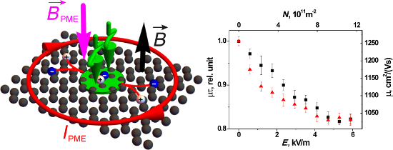
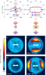
- importance. Results: Here we show a contactless method for determining these parameters in 2D semiconductors that is based on the photomagnetoelectric (PME) effect (also known as the photoelectromagnetic effect). We present calculated dependences of the PME magnetic moment, evoked in 2D Corbino configuration
- method for determining these parameters in 2D semiconductors that is based on the photomagnetoelectric (PME) effect [10]. There are a few phenomena which are or may be called PME effects. For example, in semiconductors the simultaneous action of light and magnetic field evokes specific electromotive
- -illuminated bulk semiconductors in Faraday geometry (Figure 1). In a sample illuminated by a circular spot of light, excess carriers generated by photons of appropriate energy diffuse in all directions. If this happens in a magnetic field perpendicular to the sample surface, diffusing carriers are deflected

![[Graphic 1]](/bjnano/content/inline/2190-4286-9-256-i2.svg?max-width=637&scale=1.18182) evoked by the PME circulating current in a point-illuminated 2D...
evoked by the PME circulating current in a point-illuminated 2D...

![[Graphic 7]](/bjnano/content/inline/2190-4286-9-256-i8.svg?max-width=637&scale=1.18182) vs the illumination intensity for differe...
vs the illumination intensity for differe...

![[Graphic 15]](/bjnano/content/inline/2190-4286-9-256-i16.svg?max-width=637&scale=1.18182) vs the carrier lifetime for different values ...
vs the carrier lifetime for different values ...


Two-dimensional semiconductors pave the way towards dopant-based quantum computing
Beilstein J. Nanotechnol. 2018, 9, 2668–2673, doi:10.3762/bjnano.9.249
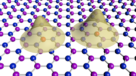
- 21941-972, Brazil 10.3762/bjnano.9.249 Abstract Since the proposal in 1998 to build a quantum computer using dopants in silicon as qubits, much progress has been made in the nanofabrication of semiconductors and the control of charge and spins in single dopants. However, an important problem remains
- Defects are a crucial concept in semiconductor technology as they provide proper carriers to intrinsically insulating semiconductors. Dopants constitute the basis for transistor operations. The miniaturisation of these devices has moved defects to the forefront of research, as their number and location
- exchange and tunnel couplings are predicted in this case. The family of 2D materials comprises an increasing number of elemental and compound semiconductors [21][22][23]. Many have been experimentally isolated already, as research activity in this area raises. In the case of non-metallic behavior, their


![[Graphic 7]](/bjnano/content/inline/2190-4286-9-249-i7.svg?max-width=637&scale=1.18182) and energy for one electron bound to a donor pair
and energy for one electron bound to a donor pair ![[Graphic 8]](/bjnano/content/inline/2190-4286-9-249-i8.svg?max-width=637&scale=1.18182) as a function of R. For R = 2a*, ...
as a function of R. For R = 2a*, ...

Impact of the anodization time on the photocatalytic activity of TiO2 nanotubes
Beilstein J. Nanotechnol. 2018, 9, 2628–2643, doi:10.3762/bjnano.9.244
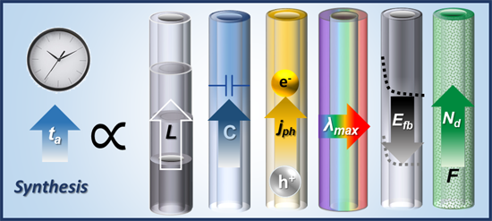
- shift not only displaces the maximum value of IPCE associated to a wavelength (λmax), but also to the absorption edge toward longer wavelengths [66]. This effect has also been observed for semiconductors where the crystalline structure has been changed by chemical doping. Other authors have reported an
- dielectric constant of the material. From the CV curves, an increase in the capacitive current was observed towards lower potential values, which is typical for a transition to the accumulation region of n-type semiconductors. The calculated values for Eg and ND are summarized in Table 3, and compared to the
- explained by a Langmuir–Hinshelwood model [86]. The oxidation mechanism for organic compounds with irradiated semiconductors has been proposed to proceed via photogenerated holes at the surface of the electrode [87][88]. The cyclic voltammograms of TNTs with ta = 0.5 h (Figure S4, Supporting Information


Exploring the photoleakage current and photoinduced negative bias instability in amorphous InGaZnO thin-film transistors with various active layer thicknesses
Beilstein J. Nanotechnol. 2018, 9, 2573–2580, doi:10.3762/bjnano.9.239
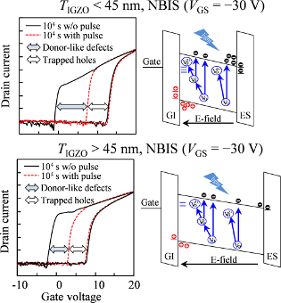
- oxygen vacancies in the bulk of the IGZO for the enhancement of electrical properties and stress stability of the TFTs, the following two aspects should be mainly considered: (i) oxidizing the densities of the defect state of oxide semiconductors to suppress charge trapping, for example by oxygen


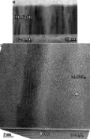
High-temperature magnetism and microstructure of a semiconducting ferromagnetic (GaSb)1−x(MnSb)x alloy
Beilstein J. Nanotechnol. 2018, 9, 2457–2465, doi:10.3762/bjnano.9.230
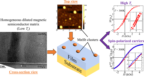
- ; nanostructured materials; thin films; Introduction Diluted magnetic semiconductors (DMS) are very promising materials for spintronic devices, because DMS offer the combination of magnetic and semiconducting properties. Currently, the most commonly studied DMS systems are those based on III–V semiconductors



Performance analysis of rigorous coupled-wave analysis and its integration in a coupled modeling approach for optical simulation of complete heterojunction silicon solar cells
Beilstein J. Nanotechnol. 2018, 9, 2315–2329, doi:10.3762/bjnano.9.216
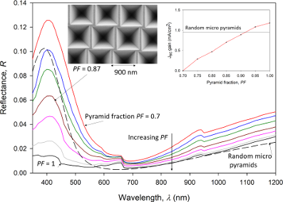
- refraction). The latter is especially important in solar cells where indirect semiconductors such as silicon (Si) are used as an absorber layer, where the absorption coefficient at the photon energy approaching the value of energy bandgap is small. Furthermore, efficient light management is important in


Metal–dielectric hybrid nanoantennas for efficient frequency conversion at the anapole mode
Beilstein J. Nanotechnol. 2018, 9, 2306–2314, doi:10.3762/bjnano.9.215
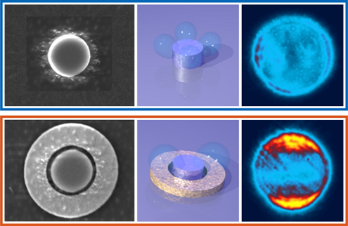
- ; plasmonics; second-harmonic generation; semiconductors; Introduction Second-harmonic generation (SHG) in bulk materials, first demonstrated by Franken and co-workers in 1961 [1], is nowadays successfully applied in a variety of disciplines. Besides its extended application in laser science for the
- symmetry. Metal-less nanophotonics based on dielectrics of high refractive index and semiconductors recently emerged as a promising alternative to plasmonic nanostructures for linear and nonlinear nanophotonic applications due to the reduced losses at optical frequencies [15]. Since in high-index
- dielectric materials the electric field penetrates deeply into the volume [16], the exploitation of large bulk nonlinearities also enables enhanced nonlinear light–matter interactions at the nanoscale. Third-harmonic generation (THG) was the first nonlinear effect observed in nanoscale semiconductors with




Hierarchical heterostructures of Bi2MoO6 microflowers decorated with Ag2CO3 nanoparticles for efficient visible-light-driven photocatalytic removal of toxic pollutants
Beilstein J. Nanotechnol. 2018, 9, 2297–2305, doi:10.3762/bjnano.9.214
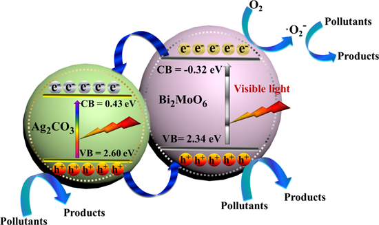
- obstacle, various methods have been developed, including doping [20][21] and the construction of heterojunctions [22][23][24][25][26][27][28][29][30][31][32][33]. Particularly, the combination of Bi2MoO6 with other semiconductors to construct heterojunction photocatalysts leads to an enhanced activity of




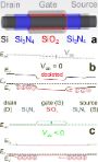
Intrinsic ultrasmall nanoscale silicon turns n-/p-type with SiO2/Si3N4-coating
Beilstein J. Nanotechnol. 2018, 9, 2255–2264, doi:10.3762/bjnano.9.210
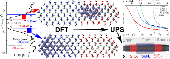
- [7][8] and dopant-associated defect states [8][9]. Modulation doping – i.e., doping of materials adjacent to semiconductors which then provide free carriers to the unperturbed semiconductor – was first used for group III–V semiconductor combinations such as GaAs/AlAs in the late 1970s [10]. Recently
- , Si modulation doping of adjacent dielectric layers based on nitrides [11] and oxides [12], in analogy to modulation doping of III–V semiconductors, were shown to be an alternative to conventional impurity doping. It would be ideal to achieve electron- (n-) or hole- (p-) type conductivity in usn-Si





Lead-free hybrid perovskites for photovoltaics
Beilstein J. Nanotechnol. 2018, 9, 2209–2235, doi:10.3762/bjnano.9.207
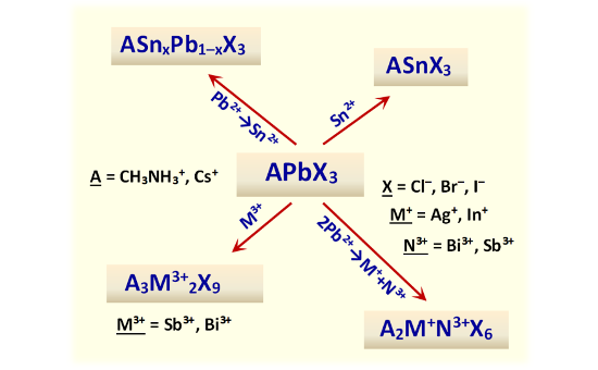
- market is dominated by silicon solar cells with top light-to-current conversion efficiencies reaching ≈27% [1]. As an alternative to the Si-based cells requiring a relatively thick absorber layer due to the indirect character of electron transitions in Si, direct-bandgap metal chalcogenide semiconductors


Electrospun one-dimensional nanostructures: a new horizon for gas sensing materials
Beilstein J. Nanotechnol. 2018, 9, 2128–2170, doi:10.3762/bjnano.9.202
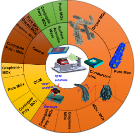
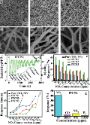
- materials used as an active sensing layer, including polymers, metal oxide semiconductors, graphene, and their composites or their functionalized forms. The material properties of these electrospun fibers and their sensing performance toward different analytes are explained in detail and correlated to the
- review and summarize the fabrication of electrospun 1D nanostructures based on diverse range of materials (including polymers, metal oxide semiconductors, graphene, and their composites or their functionalized forms) and their gas sensing performance in all available sensing architectures (including
- electrospun nanofibers as the sensing layer. These materials include: metal oxide (MOx) semiconductors (e.g., SnO2, TiO2, SiO2) [83][84], doped MOx semiconductors [4][5][6][7][8][9][10][11], composite materials made of MOx semiconducting materials (e.g., ZnO-In2O3) [86], conducting polymer-based gas sensors






Light–Matter interactions on the nanoscale
Beilstein J. Nanotechnol. 2018, 9, 2125–2127, doi:10.3762/bjnano.9.201
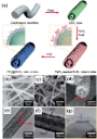
- in metals), the knowledge is still valuable for developing new strategies for light–matter interactions on the nanoscale. High refractive index dielectric [11] and semiconductor [12] nanostructures have been recently exploited as an alternative to plasmonics [13]. Dielectrics and semiconductors
Phosphorus monolayer doping (MLD) of silicon on insulator (SOI) substrates
Beilstein J. Nanotechnol. 2018, 9, 2106–2113, doi:10.3762/bjnano.9.199
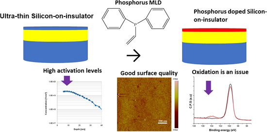
- SOI samples were prepared and MLD-doped through the methods outlined in the Experimental section. ECV was not applicable to analyse active carrier concentrations present in these samples due to their inability to etch. When etching n-type doped semiconductors, ECV requires the application of a voltage




Localized photodeposition of catalysts using nanophotonic resonances in silicon photocathodes
Beilstein J. Nanotechnol. 2018, 9, 2097–2105, doi:10.3762/bjnano.9.198
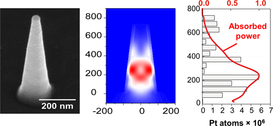
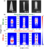
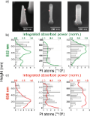
- Evgenia Kontoleta Sven H. C. Askes Lai-Hung Lai Erik C. Garnett Center for Nanophotonics, AMOLF, Science Park 104, 1098 XG Amsterdam, Netherlands 10.3762/bjnano.9.198 Abstract Nanostructured semiconductors feature resonant optical modes that confine light absorption in specific areas called “hot
- carrier. Nanostructuring the main photoactive material, e.g., a semiconductor, has proven to be a promising method for increasing the efficiency of solar fuel generation [7][8]. The higher surface to volume ratio in nanostructured semiconductors ensures the use of less material, reduces the requirements
- are simply randomly placed on semiconductor photo-electrodes with an optimized average density [20][24][25]. Photodeposition of the catalytic material with photogenerated charges from excited semiconductors has been also achieved but without a good control over the deposition sites [26][27][28][29][30


Electromigrated electrical optical antennas for transducing electrons and photons at the nanoscale
Beilstein J. Nanotechnol. 2018, 9, 1964–1976, doi:10.3762/bjnano.9.187
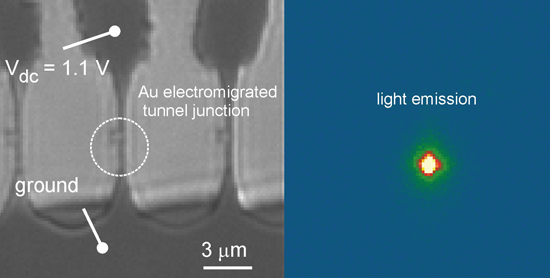
- guide photons emitted by the junctions. For the operation at visible wavelengths waveguiding structures composed of TiO2 feature interesting material properties [60][61] such as broadband transparency, high refractive index, compatibility with complementary metal-oxide semiconductors and ease of


![[Graphic 32]](/bjnano/content/inline/2190-4286-9-187-i38.svg?max-width=637&scale=1.18182) and
and ![[Graphic 33]](/bjnano/content/inline/2190-4286-9-187-i39.svg?max-width=637&scale=1.18182) are...
are...


Nonlinear effect of carrier drift on the performance of an n-type ZnO nanowire nanogenerator by coupling piezoelectric effect and semiconduction
Beilstein J. Nanotechnol. 2018, 9, 1917–1925, doi:10.3762/bjnano.9.183
- University of Science and Technology, Wuhan 430074, China 10.3762/bjnano.9.183 Abstract In piezoelectric semiconductors, electric fields drive carriers into motion/redistribution, and in turn the carrier motion/redistribution has an opposite effect on the electric field itself. Thus, carrier drift in a
- -axis; piezoelectric potential; semiconductor; zinc oxide (ZnO); Introduction An acoustic wave propagating in piezoelectric semiconductors usually stimulates electric fields that bring charge carriers into motion, and conversely, the carrier motion will produce an opposite effect on the electric fields
- and the acoustic wave itself [1][2][3][4]. This kind of interaction between an acoustic wave and carriers in piezoelectric semiconductors is called the acoustoelectric effect, which is a special case of a more general phenomenon, called wave–particle drag [4][5]. Obviously, acoustoelectric coupling of


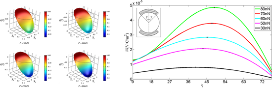
![[Graphic 46]](/bjnano/content/inline/2190-4286-9-183-i59.svg?max-width=637&scale=1.18182) and (b) boundary electric displacement Dr at Ω for different end f...
and (b) boundary electric displacement Dr at Ω for different end f...


Quantitative comparison of wideband low-latency phase-locked loop circuit designs for high-speed frequency modulation atomic force microscopy
Beilstein J. Nanotechnol. 2018, 9, 1844–1855, doi:10.3762/bjnano.9.176
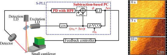
- [1]. It has been used under ultrahigh vacuum conditions for high-resolution imaging of various materials, including metals, semiconductors, metal oxides, and organic molecules [2][3][4][5]. Furthermore, recent advances in FM-AFM have enabled atom manipulation and identification at room temperature [6



Numerical analysis of single-point spectroscopy curves used in photo-carrier dynamics measurements by Kelvin probe force microscopy under frequency-modulated excitation
Beilstein J. Nanotechnol. 2018, 9, 1834–1843, doi:10.3762/bjnano.9.175
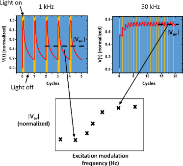
- supplied to the system and VOC decays until the charge equilibrium state is reached. The surface photovoltage (SPV), which can be seen as a local measurement of VOC in semiconductors [12], has been studied using KPFM under modulated illumination. Indeed, the investigation of the SPV evolution as a function
- of a frequency-modulated excitation source can be used to access the photo-carrier dynamics in organic, inorganic and hybrid semiconductors [3][4][5][6][7][8][9][13]. In short, as depicted in Figure 1, FMI-KPFM consist of the measurement of a surface photovoltage by KPFM (time response between a few


Improving the catalytic activity for hydrogen evolution of monolayered SnSe2(1−x)S2x by mechanical strain
Beilstein J. Nanotechnol. 2018, 9, 1820–1827, doi:10.3762/bjnano.9.173
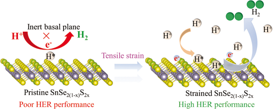
- former and latter structures are often termed as 2H-phase and 1T-phase, respectively. The stable phase for monolayer SnS2 is the 1T-phase. Alloying is an efficient approach to tune the electronic properties of semiconductors. Because of the large difference of bandgaps between SnSe2 and SnS2, the SnSe2(1
- ] and agrees well with previous results [36]. SnS2 and SnSe2 monolayers are indirect-bandgap semiconductors, as highlighted in their band structures shown in Figure 1e and Figure 1i, respectively. The valence-band maximum (VBM) is located at the M-point, whereas the conduction-band minimum (CBM) is


Multimodal noncontact atomic force microscopy and Kelvin probe force microscopy investigations of organolead tribromide perovskite single crystals
Beilstein J. Nanotechnol. 2018, 9, 1695–1704, doi:10.3762/bjnano.9.161
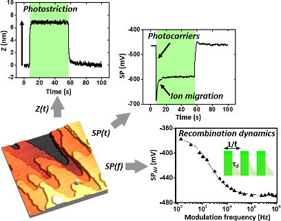
- defined as a nonthermal sample deformation under illumination. This effect is widely documented for ferroelectrics, polar and nonpolar semiconductors, and organic polymers, and it differs in origin depending on the class of material under consideration [18]. For instance, in the case of ferroelectric
- above, there is nowadays overwhelming evidence that hybrid perovskites should be treated (at least to some extent) as mixed electronic–ionic semiconductors [29]. Ion migration occurs in these materials due to the existence of anion and cation vacancies [30] and is already known to induce changes in the


Free-radical gases on two-dimensional transition-metal disulfides (XS2, X = Mo/W): robust half-metallicity for efficient nitrogen oxide sensors
Beilstein J. Nanotechnol. 2018, 9, 1641–1646, doi:10.3762/bjnano.9.156
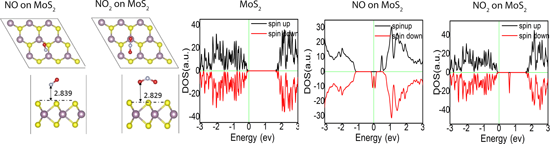
- could be uses in spintronics. But the lack of suitable materials limits the development of spintronic applications. Doping semiconductors may be applied to achieve spin-polarized currents, but this requires a complicated process. Although many materials have been predicted in theory for this purpose


Sulfur-, nitrogen- and platinum-doped titania thin films with high catalytic efficiency under visible-light illumination
Beilstein J. Nanotechnol. 2018, 9, 1629–1640, doi:10.3762/bjnano.9.155
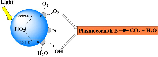
- synthesis; thin films; titanium dioxide; visible-light illumination; Introduction In recent years, titanium dioxide (TiO2) has emerged as one of the most widely investigated semiconductors [1]. Due to its favorable properties (e.g., chemical and biological stability, nontoxicity and inexpensive price) it


Spatial Rabi oscillations between Majorana bound states and quantum dots
Beilstein J. Nanotechnol. 2018, 9, 1527–1535, doi:10.3762/bjnano.9.143
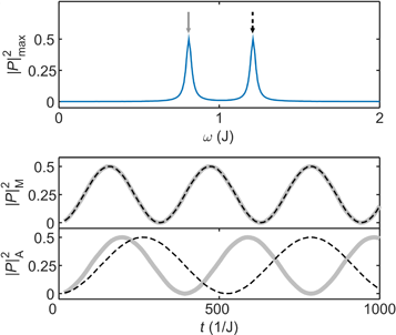
- real systems. Majorana bound states have been theoretically proposed in several systems [9][6][5][20][13], while the experiments concentrate on semiconductors with spin–orbit coupling and the superconducting gap that is induced by the superconducting proximity effect [21][24][25][19]. One promising


Cathodoluminescence as a probe of the optical properties of resonant apertures in a metallic film
Beilstein J. Nanotechnol. 2018, 9, 1491–1500, doi:10.3762/bjnano.9.140
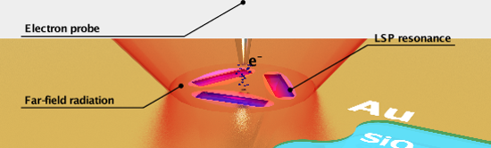
- of inorganic compounds such as ceramics, minerals and semiconductors [41][42][43]. CL has also been shown to be an invaluable tool in the investigation of optical modes of nanostructures [44]. These include characterising the plasmonic modes of silver nanoparticles [45] and resonant modes of single





