Search results
Search for "band gap" in Full Text gives 271 result(s) in Beilstein Journal of Nanotechnology. Showing first 200.
Thickness-dependent photoelectrochemical properties of a semitransparent Co3O4 photocathode
Beilstein J. Nanotechnol. 2018, 9, 2432–2442, doi:10.3762/bjnano.9.228

- regarding low-cost and reliable PEC cells [1][2][3][4][5][6][7][8]. For a widespread application of PEC cells, the photoelectrodes need to fulfill the criteria of (i) a low band gap (1.7–2.2 eV), (ii) low resistivity, (iii) low cost, (iv) corrosion stability and (v) a correct alignment of band edges with
- in Figure 5c supports the claim of porosity in the grown Co3O4 film and the void-free interface between Co3O4/FTO. Further, we estimated the thickness-dependent band-gap energies (Eg) of the Co3O4 samples using Tauc’s relation as shown in Figure 5d. The coexistence of bandgaps two distinct band gaps
- the Co3O4/FTO samples. Here t, T, λ, Eg, VFB and NA are the thickness of the Co3O4 layer, transmittance, photon wavelength, band gap, flat-band potential, and acceptor carrier concentration, respectively. Supporting Information Supporting Information File 146: Additional experimental data


Metal–dielectric hybrid nanoantennas for efficient frequency conversion at the anapole mode
Beilstein J. Nanotechnol. 2018, 9, 2306–2314, doi:10.3762/bjnano.9.215

- amplification [22] and enhanced Raman scattering [23] have been recently suggested. In this framework, AlxGa1−xAs, a III–V semiconductor, has become a popular material for nonlinear photonics thanks to its non-centrosymmetric structure and other important key assets including: i) a large band gap enabling TPA


Hierarchical heterostructures of Bi2MoO6 microflowers decorated with Ag2CO3 nanoparticles for efficient visible-light-driven photocatalytic removal of toxic pollutants
Beilstein J. Nanotechnol. 2018, 9, 2297–2305, doi:10.3762/bjnano.9.214

- absorption of the Ag2CO3/Bi2MoO6 heterostructures was substantially improved owing through the introduction of Ag2CO3 nanoparticles. Ag/Ag2CO3/Bi2MoO6 [32], Ag2MoO4/Bi2MoO6 [22], and Ag2CO3/Bi2MoO6 heterostrutures are VLD photocatalysts. The band gap energy (Eg) can be estimated from the Tauc plot: (αhν) = A


Lead-free hybrid perovskites for photovoltaics
Beilstein J. Nanotechnol. 2018, 9, 2209–2235, doi:10.3762/bjnano.9.207


Electrospun one-dimensional nanostructures: a new horizon for gas sensing materials
Beilstein J. Nanotechnol. 2018, 9, 2128–2170, doi:10.3762/bjnano.9.202

- type of ZnO doping is with indium, for which the product is called “IZO”. When the amount of indium is greater than 0.05, amorphous In2O3 forms and leads to a pronounced decrease in grain size. The optical band gap energy of IZO NTs also decreases with increased doping levels. Doped indium atoms may


Light–Matter interactions on the nanoscale
Beilstein J. Nanotechnol. 2018, 9, 2125–2127, doi:10.3762/bjnano.9.201

- graphene with electromagnetic radiation is fascinating due to the two-dimensional confinement of electrons and the exceptional band structure of graphene. Graphene has a simple band structure with zero band gap, but its optical response is nontrivial. Subsequently, other two-dimensional (2D) materials
Spin-coated planar Sb2S3 hybrid solar cells approaching 5% efficiency
Beilstein J. Nanotechnol. 2018, 9, 2114–2124, doi:10.3762/bjnano.9.200

- ; hole transport material; solar cell; Introduction Antimony sulfide (Sb2S3) is a promising high band gap light absorber for solar cells [1][2][3][4][5]. The record efficiency of 7.5% [6] is comparable to that of other less investigated materials, such as the best lead-free perovskites [7], Cu2O [8] and
- -bandgap region [53][54][55][56] including band tails that yield the Urbach energy as a measure of disorder as well as the detection of (optically active) defects in the band gap which can act as recombination centers in a solar cell. The Sb-TU process shows a slight increase in uncovered substrate area
- conditions thus closely resemble those of the fabricated solar cells. The results for different crystallization temperatures in the Sb-TU process are shown in Figure 3c. For the sample crystallized at 265 °C and 300 °C, the measurement signal quickly saturates at energies above the band gap. At low energies


A scanning probe microscopy study of nanostructured TiO2/poly(3-hexylthiophene) hybrid heterojunctions for photovoltaic applications
Beilstein J. Nanotechnol. 2018, 9, 2087–2096, doi:10.3762/bjnano.9.197

- can easily form nanostructures, such as nanoporous layers, nanowires or nanocolumns [5][11][12]. Because of its large band gap (3.2 eV [13]), light absorption is carried out by an organic or inorganic dye. The nanostructuration of the acceptor material is crucial for the cell performance [11], as it


The role of the Ge mole fraction in improving the performance of a nanoscale junctionless tunneling FET: concept and scaling capability
Beilstein J. Nanotechnol. 2018, 9, 1856–1862, doi:10.3762/bjnano.9.177

- combined using Matthiessen’s formula. Accordingly, the Lombardi model (CVT) is used to express the carrier mobility in the channel [27]. Moreover, the intrinsic parameters of the materials (Si, Si1−xGex and Ge) such as band gap, mobility and the density of states were considered to be dependent on the Ge
- conventional design with Si channel shows a reduced OFF-state current compared to that of the investigated heterochannel designs, which is mainly due to the high band-gap energy and the low electron mobility associated to Si. On the other hand, the conventional Ge-DG-JL TFET design provides higher ON-state
- current. This is due to the smaller band gap energy of Ge, yielding a higher tunneling efficiency. Moreover, the higher electron mobility of Ge (3900 cm2·V−1·s−1) contributes to the increased drain current at the threshold voltage as compared to the conventional design with silicon (1400 cm2·V−1·s−1


Improving the catalytic activity for hydrogen evolution of monolayered SnSe2(1−x)S2x by mechanical strain
Beilstein J. Nanotechnol. 2018, 9, 1820–1827, doi:10.3762/bjnano.9.173

- . In this work, the electronic properties and catalytic behaviour for HER of SnSe2(1−x)S2x (x = 0, 0.125, 0.25, 0.375, 0.5, 0.625, 0.750, 0.875 and 1.0) monolayers were investigated by density functional theory (DFT). It was shown that band gap and catalytic activity of these alloys can be continuously
- , Figure 1g and Figure 1h, respectively. The substitution of S with Se does not affect the indirect bandgap semiconducting characteristics; however, the band gap is tuned with changing the content of Se, as shown in Figure 1d with the indirect band gap decreasing with increasing Se content. These results
- the top of S are close to zero at a tensile strain of 10%; thus, strain can be used to improve the catalytic activity for HER. As shown in Figure 4, also the band gaps show great dependence on the applied strain. The band gap decreases from 1.59 to 1.48 eV for the SnS2 monolayer as the compressive


Controllable one-pot synthesis of uniform colloidal TiO2 particles in a mixed solvent solution for photocatalysis
Beilstein J. Nanotechnol. 2018, 9, 1715–1727, doi:10.3762/bjnano.9.163

- explored semiconducting material that exists in abundance from natural resources. It has a wide range of applications including bio-separation, sensors, energy storage, catalysis and photocatalysis [1][2][3][4][5][6][7][8][9][10][11]. Due to its wide band gap energy (3.0–3.2 eV) between the conduction and
- . First, the semiconductor photocatalyst can absorb photon energy that is greater than its band gap and electrons in the valance band can be exited to the conduction band, resulting in photoexcited electron–hole pairs. Then, the photo-exited electron–hole can move to the surface of the photocatalyst
- without charge recombination. Finally, each charge carrier can be consumed for surface redox reactions [9][15]. To achieve high performance in the overall photocatalysis system, the efficiency of each step should be improved [13]. Regarding the point of light absorption, the band gap energy range of the


Multimodal noncontact atomic force microscopy and Kelvin probe force microscopy investigations of organolead tribromide perovskite single crystals
Beilstein J. Nanotechnol. 2018, 9, 1695–1704, doi:10.3762/bjnano.9.161

- , including a direct band gap, high absorption coefficient, large and balanced carrier mobility, high diffusion length, long carrier lifetime and high photoluminescence quantum yield. Within a few years of their discovery, these materials were successfully used to develop photovoltaic cells [2] with power


Free-radical gases on two-dimensional transition-metal disulfides (XS2, X = Mo/W): robust half-metallicity for efficient nitrogen oxide sensors
Beilstein J. Nanotechnol. 2018, 9, 1641–1646, doi:10.3762/bjnano.9.156

- NOx (x = 1, 2; Figure 2). Pristine 2D XS2 (X = Mo, W) has a band gap of approximately 2 eV. In the case of NO adsorbed on XS2 (X = Mo, W), a large density of spin-up electrons appear around the Fermi level, while no spin-down electrons appear. Analyzing the PDOS of a WS2 nanosheet with adsorbed NO


Sulfur-, nitrogen- and platinum-doped titania thin films with high catalytic efficiency under visible-light illumination
Beilstein J. Nanotechnol. 2018, 9, 1629–1640, doi:10.3762/bjnano.9.155

- , band gap measurements). The photocatalytic activity of the prepared thin films was determined by measuring the degradation rate of plasmocorinth B (PB), an organic pigment used in the textile industry, which can pose an environmental risk when expelled into wastewater. A kinetic model for adsorption
- rather there exists an optimal particle size for pure nanocrystalline TiO2 [19]. This is due to surface recombination of electron–hole pairs in samples with particle sizes smaller than 6 nm. One of the main drawbacks of using TiO2 as a photocatalyst is the width of its band gap (3.2 eV), which means the
- of the band gap by introducing a new energy level close to the valence band. Nitrogen doping can also create impurity energy levels above the valence band, thus effectively also narrowing the band gap [35][36]. Illumination with visible light can then excite electrons from impurity energy levels into


Sheet-on-belt branched TiO2(B)/rGO powders with enhanced photocatalytic activity
Beilstein J. Nanotechnol. 2018, 9, 1550–1557, doi:10.3762/bjnano.9.146

- . The TGN-branch 4 h sample exhibits almost the same absorbance (Figure 6a) and the same band gap of 2.87 eV (Figure 6b) compared to TGN. This can be attributed to the same phase composition of TiO2(B) in both samples. The evaluated band gap of 2.87 eV for TiO2(B) agrees with that (2.9 eV) reported by
- Kandiel et al. [25]. This band gap value is smaller than that of 3.2 eV for bulk anatase TiO2 [27]. Chakraborty et al. also reported that the absorption band edge of the pure TiO2(B) is located at a relatively longer wavelength compared to that of the pure anatase TiO2 [21]. The low temperature nitrogen
- , and (d) O 1s for sample TGN-branch 4 h. (a) UV–vis diffuse reflectance spectra of TGN and TGN-branch 4 h. (b) Re-plotting of (a) in the α1/2 ~ hν coordinate to evaluate the corresponding band gap, assuming an indirect transition between bands for TiO2. Photodegradation of phenol in the presence of


Photoluminescence of CdSe/ZnS quantum dots in nematic liquid crystals in electric fields
Beilstein J. Nanotechnol. 2018, 9, 1544–1549, doi:10.3762/bjnano.9.145

- University (Minsk). The shell of ZnS with wider band gap prevents a degradation of the CdSe core by passivation of broken bonds on its surface. Quantum dots were covered with а layer of surface-active trioctylphosphine oxide (TOPO) molecules. The nematic alkylcyanobiphenyl-based liquid crystal ZhK-1289
- dependence on two independent, but spectrally overlapping, processes. The first process involves the recombination of the so-called “internal” exciton with energy close to the width of the band gap and a decay time of about 20–30 ns, depending on the size of the quantum dots. The second process is associated


Cr(VI) remediation from aqueous environment through modified-TiO2-mediated photocatalytic reduction
Beilstein J. Nanotechnol. 2018, 9, 1448–1470, doi:10.3762/bjnano.9.137

- surface of the semiconductor. When photons with energy greater than the band gap energy of the semiconductor photocatalyst (SP) are absorbed, photogenerated electrons are excited to conduction band (CB) leaving behind holes at the valence band (VB) as per Equation 1: These photogenerated species
- cases, hole scavengers are used to facilitate the electron–hole separation process. However, application of TiO2 in photocatalysis is largely restricted mainly due to the following reasons. (i) The wide band gap of 3.2 eV causes excitation of electrons from the valence band under irradiation of UV light
- , or B narrows the band gap either by creating a mid-band gap or shifting the valence band to upper positions, resulting in a redshift. Even modification of titania with semiconductor oxides or sulfides improves the light absorption. It was evident from UV–vis DRS spectra that light absorption is


Robust midgap states in band-inverted junctions under electric and magnetic fields
Beilstein J. Nanotechnol. 2018, 9, 1405–1413, doi:10.3762/bjnano.9.133

- Figure 5 it may be surprising to see that the Landau bands shift below the band edge, leading to the apparent and erroneous belief that the latter enter the band gap. The effect of the electric field is to bend the constant band edges shown in Figure 1a upwards due to the presence of the electrostatic
- potential eFz, and so the Landau levels of the conduction band can move towards lower energies as long as the corresponding wave functions are not inside the band gap in position space. Finally, it deserves consideration the previous discussion for low values of . As we can see in Figure 6, the parabolic

![[Graphic 1]](/bjnano/content/inline/2190-4286-9-133-i26.svg?max-width=637&scale=1.18182) and
and ![[Graphic 2]](/bjnano/content/inline/2190-4286-9-133-i27.svg?max-width=637&scale=1.18182) band-edge profile of an abrupt band-inverted junction with aligned and same-sized gaps, l...
band-edge profile of an abrupt band-inverted junction with aligned and same-sized gaps, l...


![[Graphic 35]](/bjnano/content/inline/2190-4286-9-133-i60.svg?max-width=637&scale=1.18182) and b = 0.5 as a function of the electric field. It is important...
and b = 0.5 as a function of the electric field. It is important...

Predicting the strain-mediated topological phase transition in 3D cubic ThTaN3
Beilstein J. Nanotechnol. 2018, 9, 1399–1404, doi:10.3762/bjnano.9.132

- Chunmei Zhang Aijun Du School of Chemistry, Physics and Mechanical Engineering, Queensland University of Technology, Gardens Point Campus, QLD 4001, Brisbane, Australia 10.3762/bjnano.9.132 Abstract The cubic ThTaN3 compound has long been known as a semiconductor with a band gap of approximately
- 1 eV, but its electronic properties remain largely unexplored. By using density functional theory, we find that the band gap of ThTaN3 is very sensitive to the hydrostatic pressure/strain. A Dirac cone can emerge around the Γ point with an ultrahigh Fermi velocity at a compressive strain of 8
- %. Interestingly, the effect of spin–orbital coupling (SOC) is significant, leading to a band gap reduction of 0.26 eV in the ThTaN3 compound. Moreover, the strong SOC can turn ThTaN3 into a topological insulator with a large inverted gap up to 0.25 eV, which can be primarily attributed to the inversion between


Computational exploration of two-dimensional silicon diarsenide and germanium arsenide for photovoltaic applications
Beilstein J. Nanotechnol. 2018, 9, 1247–1253, doi:10.3762/bjnano.9.116

- . Furthermore, band-gap tuning is also possible by application of tensile strain. Our results highlight a new family of 2D materials with great potential for solar cell applications. Keywords: density functional theory (DFT); photovoltaic applications; solar cell; two-dimensional semiconductors; Introduction
- ]. However, they did not report the band structure or the band gap values of these materials. Later, Wu et al. performed theoretical studies on silicon and germanium arsenides [9] to predict and reaffirm that m-SiAs/GeAs and o-SiAs2/GeAs2 are indeed semiconductors. The studies were based on band-structure
- the same IV–V group combination, we focus our study on two-dimensional SiAs2 and GeAs2 and compare them with their bulk counter parts with regard to electronic band structure, phonon-vibration frequencies, optical properties, band gap modulation behavior and predict their potential applications


Theoretical study of strain-dependent optical absorption in a doped self-assembled InAs/InGaAs/GaAs/AlGaAs quantum dot
Beilstein J. Nanotechnol. 2018, 9, 1075–1084, doi:10.3762/bjnano.9.99

- gap and confinement energies work with each other, whereas when the height is changed, the band gap and confinement energies work against each other. Increasing the mole fraction if In in the strain controlling layer works in the same way as increasing the dot diameter and changes the strain leading
- NEMO5 and used to simulate characteristics of an InAs/GaAs/AlAs quantum dot systems. Increasing the dot diameter results in a shift of the absorption peaks towards longer wavelengths, while increasing the dot height does not have a significant effect on wavelength. When the diameter is changed, the band


Non-equilibrium electron transport induced by terahertz radiation in the topological and trivial phases of Hg1−xCdxTe
Beilstein J. Nanotechnol. 2018, 9, 1035–1039, doi:10.3762/bjnano.9.96

- . 53, 119991 Moscow, Russia 10.3762/bjnano.9.96 Abstract Terahertz photoconductivity in heterostructures based on n-type Hg1−xCdxTe epitaxial films both in the topological phase (x < 0.16, inverted band structure, zero band gap) and the trivial state (x > 0.16, normal band structure) has been studied
- . It was assumed that the negative photoresponse in the samples with the normal band structure is most likely related to the electron gas heating, while the positive photoconductivity in the zero band gap mercury cadmium telluride was reasonable to associate with interband transitions. In this work, we


An implementation of spin–orbit coupling for band structure calculations with Gaussian basis sets: Two-dimensional topological crystals of Sb and Bi
Beilstein J. Nanotechnol. 2018, 9, 1015–1023, doi:10.3762/bjnano.9.94

- recently added to the growing library of 2D crystals. Its recent isolation and characterization [33], is bringing this material into the focus of the research community. Several DFT studies on this material have predicted a number of exciting physico-chemical properties, including a tunable band gap with


Cyclodextrin inhibits zinc corrosion by destabilizing point defect formation in the oxide layer
Beilstein J. Nanotechnol. 2018, 9, 936–944, doi:10.3762/bjnano.9.86
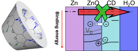
- reactions, forming precipitates such as hydrated zinc oxide [15]. ZnO is naturally an n-type semiconductor with a band gap of 3.4 eV [20]. Oxides formed in an aerated corrosion process are typically defect-rich oxides [21], especially in the presence of Cl− [15]. Consequently, the products remain initially
- − HOMO-CDonset to be 1.85 eV. The band gap of β-CD has been reported to be 12.44 eV [38], and judging from the position of the Fermi level, β-CD is in the same role as a p-type system. Charge dislocation must lead to hole accumulation at the ZnO side, i.e., depletion of negative charge. On the β-CD side


Comparative study of antibacterial properties of polystyrene films with TiOx and Cu nanoparticles fabricated using cluster beam technique
Beilstein J. Nanotechnol. 2018, 9, 861–869, doi:10.3762/bjnano.9.80

- ], and they are also cheaper compared to silver. These particles mainly show bactericidal effects through mechanisms (i) and (iii). Among the metal oxides, TiO2 is the best-known and most widely used semiconductor material with a wide band gap that under UV illumination generates electron–hole pairs


