Search results
Search for "density of states" in Full Text gives 195 result(s) in Beilstein Journal of Nanotechnology.
The effect of translation on the binding energy for transition-metal porphyrines adsorbed on Ag(111) surface
Beilstein J. Nanotechnol. 2019, 10, 706–717, doi:10.3762/bjnano.10.70

- exchange–correlation functionals, we compared the density of states obtained using BH or the Perdew–Burke–Ernzerhoff (PBE) functional [63]. The data presented in Supporting Information File 1, Figure S1, shows that the DOS are almost identical for VPP, MnPP and FePP, while for three other molecules a
- effect on the electronic structure of the molecule is strong enough to change the magnetization of the adsorbed molecule (see Supporting Information File 1, Figure S5 left panel, for details of the projected density of states of NiPP at the “i” and “b” points). The density of states of the “i” and “b
- ” positions shows that in the bridge position the 3d orbital at 1.3 eV above the Fermi level is relatively localized from an energetically point of view. At the “i” position it interacts with the silver substrate, leading to a very broad density of states that is in the vicinity of the Fermi level


![[Graphic 1]](/bjnano/content/inline/2190-4286-10-70-i1.svg?max-width=637&scale=1.18182) , for all systems and relative molecule–surface positions. Right: symm...
, for all systems and relative molecule–surface positions. Right: symm...


![[Graphic 7]](/bjnano/content/inline/2190-4286-10-70-i7.svg?max-width=637&scale=1.18182) for selected TMPP systems (M = V, Mn, Co; red: positive values, blue: negative value...
for selected TMPP systems (M = V, Mn, Co; red: positive values, blue: negative value...
A carrier velocity model for electrical detection of gas molecules
Beilstein J. Nanotechnol. 2019, 10, 644–653, doi:10.3762/bjnano.10.64

- . Thus, the energy dispersion relation of AGNR is developed considering the molecular adsorption effect using a tight binding (TB) method. The carrier velocity is calculated based on the density of states (DOS) and carrier concentration (n) to obtain I–V characteristics and to monitor its variation in
- path forward to overcome the constraints of experimental approaches. The adsorption of gas molecules can modulate different electrical and physical properties of the GNRs, such as density of states (DOS), carrier concentration, carrier velocity, I–V characteristics, and energy band structure. On the
- theoretical studies have confirmed that the velocity of the electrons is a function of carrier concentration (n) and density of states (DOS). The electron’s velocity is directly proportional to the DOS at any instance. The carrier velocity in the AGNR can be obtained by the accumulative velocity of all the


Coexisting spin and Rabi oscillations at intermediate time regimes in electron transport through a photon cavity
Beilstein J. Nanotechnol. 2019, 10, 606–616, doi:10.3762/bjnano.10.61

- single-particle components, their probability distribution in the contact area of the short quantum wire, and depends on their energy and the density of states of the leads at the corresponding energy. The leads are quasi-1D with a sharply peaked density of states near the subband bottoms. Orbital


![[Graphic 40]](/bjnano/content/inline/2190-4286-10-61-i49.svg?max-width=637&scale=1.418184) and photon
and photon ![[Graphic 41]](/bjnano/content/inline/2190-4286-10-61-i50.svg?max-width=637&scale=1.418184) content in the open central system as a function of time. In additio...
content in the open central system as a function of time. In additio...


![[Graphic 60]](/bjnano/content/inline/2190-4286-10-61-i69.svg?max-width=637&scale=1.418184)
![[Graphic 61]](/bjnano/content/inline/2190-4286-10-61-i70.svg?max-width=637&scale=1.418184)
![[Graphic 62]](/bjnano/content/inline/2190-4286-10-61-i71.svg?max-width=637&scale=1.418184) and
and ![[Graphic 63]](/bjnano/content/inline/2190-4286-10-61-i72.svg?max-width=637&scale=1.418184) i...
i...

![[Graphic 76]](/bjnano/content/inline/2190-4286-10-61-i85.svg?max-width=637&scale=1.418184) in the steady state. The cavity pho...
in the steady state. The cavity pho...
Mo-doped boron nitride monolayer as a promising single-atom electrocatalyst for CO2 conversion
Beilstein J. Nanotechnol. 2019, 10, 540–548, doi:10.3762/bjnano.10.55

- preferable to H2O. As the projected density of states (Supporting Information File 1, Figure S3) shows, we note that there is an overlapping of the p- and d-orbitals of the CO2 absorbed structure located at around −1.36/−0.46 eV. This is the result of the strong interaction between CO2 and Mo-doped BN


Transport signatures of an Andreev molecule in a quantum dot–superconductor–quantum dot setup
Beilstein J. Nanotechnol. 2019, 10, 363–378, doi:10.3762/bjnano.10.36

- obtained from the leading-order term in Fermi’s golden rule as where α {L,R} is the lead index, is a characteristic tunneling rate between the normal lead Nα and the SC–QD–SC system, ρNα is the density of states at the Fermi energy in the lead Nα, and is the Fermi function. We calculate the stationary


Investigation of CVD graphene as-grown on Cu foil using simultaneous scanning tunneling/atomic force microscopy
Beilstein J. Nanotechnol. 2018, 9, 2953–2959, doi:10.3762/bjnano.9.274

- complicated as it could be interpreted as a map of the local charge density of states of the surface at the Fermi level [6]. Therefore, depending on tip type and its electronic charge state, different relative contrasts of the atoms on the surface, including even reversal of contrast, are obtained in STM
- inequivalent. Since, b atoms have a greater contribution to the density of states close to Fermi energy compared to a atoms, they are imaged as bright spots at low bias voltages based on the STM investigations. These b atoms form a new larger triangular structure in STM images (two lattice points in this
- slight difference in two different regions. Also, there is a small gradual increase in height starting midway through the STM image, which suggests a change in overall local density of states (LDOS) or topography. Line profiles of the force and STM topography in the two regions are given in the figure


Intrinsic ultrasmall nanoscale silicon turns n-/p-type with SiO2/Si3N4-coating
Beilstein J. Nanotechnol. 2018, 9, 2255–2264, doi:10.3762/bjnano.9.210

- Moore’s law to reach the Si-crystallization limit of ca. 1.5 nm [15]. In our present work, we prove by hybrid-density functional theory (h-DFT) simulations and synchrotron-based long-term ultraviolet photoelectron spectroscopy (UPS) that usn-Si indeed can have a massive ΔE of their electronic density of
- states (DOS) when embedded in SiO2 or Si3N4. We use further h-DFT results of a Si-nanowire (NWire) covered in SiO2 and Si3N4 to examine the device behaviour of an undoped Si-NWire FET based solely on CMOS-compatible materials (e.g., Si, SiO2, Si3N4) using the nonequilibrium Green’s function (NEGF


Dumbbell gold nanoparticle dimer antennas with advanced optical properties
Beilstein J. Nanotechnol. 2018, 9, 2188–2197, doi:10.3762/bjnano.9.205

- additionally, which is usually blue-shifted from the LSPR. As a consequence of these dependencies, the effective local density of states (LDOS) varies. The observed spectral variations for geometrically similar dimers are likely correlated to the spread in the fluorescence enhancement factor. In principle


Spin-coated planar Sb2S3 hybrid solar cells approaching 5% efficiency
Beilstein J. Nanotechnol. 2018, 9, 2114–2124, doi:10.3762/bjnano.9.200

- absorption coefficient of a thin-film is measured over several orders of magnitude [52][53] which cannot be achieved by standard transmission–reflection measurements using an UV–vis photospectrometer. The large dynamic range of PDS makes it a powerful tool for to study the density of states in the sub
- attributed to interference in the smooth films – which did not fully cancel out during data analysis – instead of actual variations in the materials’ density of states in the sub-bandgap region. The negative impact of the increased defect density on device performance is confirmed by comparing solar cells


Metal-free catalysis based on nitrogen-doped carbon nanomaterials: a photoelectron spectroscopy point of view
Beilstein J. Nanotechnol. 2018, 9, 2015–2031, doi:10.3762/bjnano.9.191

- zero-gap semiconductor). This peculiarity represents one of the biggest challenges for its use in concrete applications, because it results in a very low density of states (DOS) at the Fermi level for typical doping levels, making graphene an intrinsically inert material. To overcome these issues
- , several strategies have been employed to tailor the properties of graphene. Being very sensitive to local perturbations, any modification of the lattice or adsorption of foreign atoms or molecules produce sudden evident changes in the density of states that can be monitored by the shift of the Dirac cone
- the electronic states of graphene. In general, point defects generate localized states at the Fermi level, easily identifiable as protrusion by scanning tunneling microscopy (STM) [56], while carbon vacancies are responsible for an opening of the energy gap [57]. The increase in the density of states


The role of the Ge mole fraction in improving the performance of a nanoscale junctionless tunneling FET: concept and scaling capability
Beilstein J. Nanotechnol. 2018, 9, 1856–1862, doi:10.3762/bjnano.9.177

- combined using Matthiessen’s formula. Accordingly, the Lombardi model (CVT) is used to express the carrier mobility in the channel [27]. Moreover, the intrinsic parameters of the materials (Si, Si1−xGex and Ge) such as band gap, mobility and the density of states were considered to be dependent on the Ge


Improving the catalytic activity for hydrogen evolution of monolayered SnSe2(1−x)S2x by mechanical strain
Beilstein J. Nanotechnol. 2018, 9, 1820–1827, doi:10.3762/bjnano.9.173

- increases upon application of tensile strain because the valence band and conduction band move upward and downward in energy, respectively. Previous reports showed that H adsorption depends on the density of states near the Fermi energy level [57][58], with the adsorption being enhanced as the d-band centre


A zero-dimensional topologically nontrivial state in a superconducting quantum dot
Beilstein J. Nanotechnol. 2018, 9, 1705–1714, doi:10.3762/bjnano.9.162

- electron dispersion in the two superconducting leads. In the following we furthermore assume that the bare electron dispersion varies in the interval [−D,D] and that the density of states is ρ0 = 1/(2D) with 2D the total bandwidth. The tunneling between the dot and the leads is described by the tunnel


Josephson effect in junctions of conventional and topological superconductors
Beilstein J. Nanotechnol. 2018, 9, 1659–1676, doi:10.3762/bjnano.9.158

- and take real-valued tunnel amplitudes λS/TS, see Figure 1a, using a gauge where the superconducting phase difference appears via the QD–TS tunneling term. These tunnel amplitudes contain density-of-states factors for the respective leads. The operator expression for the current flowing through the


![[Graphic 75]](/bjnano/content/inline/2190-4286-9-158-i137.svg?max-width=637&scale=1.18182) = 1 in Figure 6, for different bulk Zeeman fields Vx (in meV) near the crit...
= 1 in Figure 6, for different bulk Zeeman fields Vx (in meV) near the crit...


Free-radical gases on two-dimensional transition-metal disulfides (XS2, X = Mo/W): robust half-metallicity for efficient nitrogen oxide sensors
Beilstein J. Nanotechnol. 2018, 9, 1641–1646, doi:10.3762/bjnano.9.156

- . The binding position and adsorption energy are analyzed in detail. In terms of the projected density of states (PDOS) and orbital contribution, our results offer a deep insight into the Fermi-level pinning mechanism. In addition, we expand the calculations to other 2D layered materials including GaS


Interplay between pairing and correlations in spin-polarized bound states
Beilstein J. Nanotechnol. 2018, 9, 1370–1380, doi:10.3762/bjnano.9.129

- -of-plane spin–orbit field, respectively, and satisfy . Solving numerically the BdG equations (Equation 6) we can determine the local order parameter χi and occupancy niσ where f(ω) = [1 + exp(ω/kBT)]−1. In what follows, we shall inspect the spin-resolved local density of states For its numerical
- observe a constructive influence of the Majorana quasiparticle on opposite-spin ↓ electrons. Figure 9 shows evolution of the spectral function ρ↑(ω) for various couplings tm. In the weak-coupling limit we clearly observe a reduction (by half) of the initial density of states. With increasing tm the


![[Graphic 23]](/bjnano/content/inline/2190-4286-9-129-i39.svg?max-width=637&scale=1.18182) obtained for |J| < Jc in the absence of spin–orbit coupling (le...
obtained for |J| < Jc in the absence of spin–orbit coupling (le...

![[Graphic 26]](/bjnano/content/inline/2190-4286-9-129-i42.svg?max-width=637&scale=1.18182) as a function of the r...
as a function of the r...


Andreev spectrum and supercurrents in nanowire-based SNS junctions containing Majorana bound states
Beilstein J. Nanotechnol. 2018, 9, 1339–1357, doi:10.3762/bjnano.9.127

- , a highly transmissive interface between the nanowire and the superconductor is required, so that electrons can tunnel between these two systems [13][14][15][16]. This results in a superconducting nanowire, with a well-defined induced hard gap (namely, without residual quasiparticle density of states


![[Graphic 44]](/bjnano/content/inline/2190-4286-9-127-i52.svg?max-width=637&scale=1.18182) in a short SNS j...
in a short SNS j...


![[Graphic 73]](/bjnano/content/inline/2190-4286-9-127-i81.svg?max-width=637&scale=1.18182) = 0 (a,b)...
= 0 (a,b)...


![[Graphic 84]](/bjnano/content/inline/2190-4286-9-127-i92.svg?max-width=637&scale=1.18182) ), fo...
), fo...


![[Graphic 119]](/bjnano/content/inline/2190-4286-9-127-i127.svg?max-width=637&scale=1.18182) at B = 1.5Bc. Contributions to the supercurrent for (a,b) short and ...
at B = 1.5Bc. Contributions to the supercurrent for (a,b) short and ...

![[Graphic 163]](/bjnano/content/inline/2190-4286-9-127-i171.svg?max-width=637&scale=1.18182) ), in (a,b) a short and (c,d) a long junction. (a,...
), in (a,b) a short and (c,d) a long junction. (a,...

![[Graphic 175]](/bjnano/content/inline/2190-4286-9-127-i183.svg?max-width=637&scale=1.18182) ), in (a,b) a...
), in (a,b) a...

![[Graphic 186]](/bjnano/content/inline/2190-4286-9-127-i194.svg?max-width=637&scale=1.18182) ) in (a,b) a short and (c,d) a long ...
) in (a,b) a short and (c,d) a long ...
Inverse proximity effect in semiconductor Majorana nanowires
Beilstein J. Nanotechnol. 2018, 9, 1184–1193, doi:10.3762/bjnano.9.109

- resulting restrictions on the operation of Majorana-based devices. A strong paramagnetic effect for electrons entering the semiconductor together with spin–orbit coupling and van Hove singularities in the electronic density of states in the wire are responsible for the suppression of superconducting
- analogous to the one used in the phenomenological model. On top of that it gives the gap dependence on the transparency of the interface between the wire and the s-wave superconductor and chemical potential via density of states (DOS). Another important point is that the exchange of electrons between the


Thermoelectric current in topological insulator nanowires with impurities
Beilstein J. Nanotechnol. 2018, 9, 1156–1161, doi:10.3762/bjnano.9.107

- velocity vn(E) and density of states ρn(E) of a given mode n at energy E [36]. This product is a constant vn(E)ρn(E) = 1/h, irrespective of the form of εn(k), which leads to the well-known conductance quantum e2/h. For infinitely long, ballistic systems all channels are perfectly transmitted Tn = 1, so one


Cyclodextrin inhibits zinc corrosion by destabilizing point defect formation in the oxide layer
Beilstein J. Nanotechnol. 2018, 9, 936–944, doi:10.3762/bjnano.9.86
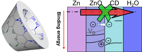
- , defect levels affect the VBonset and VBmax energy positions differently, consequently altering the density of states in the VB region. Altered density of states leads to different charge carrier densities at the interface and a decrease in potential barrier for charge dislocation.) From the magnitude of


The effect of atmospheric doping on pressure-dependent Raman scattering in supported graphene
Beilstein J. Nanotechnol. 2018, 9, 704–710, doi:10.3762/bjnano.9.65

- and copper [19] which are terminated after the transfer. Besides, this may lead to different values of the average graphene–substrate distance resulting in deviation of the density of states (DOS) from a simple Dirac cone [16] and a consequent shift of the Dirac point energy, leading to different


Revealing the interference effect of Majorana fermions in a topological Josephson junction
Beilstein J. Nanotechnol. 2018, 9, 520–529, doi:10.3762/bjnano.9.50

- the local density of states (DOS) in a topological Josephson junction. We show that the well-known 4π Josephson effect originates from the interference effect between two Majorana fermions (MFs) that are localized at the Josephson junction. In addition, the DOS for electrons (holes) shows the 4π
- interference effect of the MFs as well as the DOS by combining Andreev reflection with the electron transmission process. Keywords: density of states; fractional Josephson effect; Majorana fermion; Introduction After Kitaev reported that Majorana fermions (MFs) can appear as quasi-particle states at the ends
- topological superconductors as shown in Figure 1a. Unlike previous studies, we focus on the density of states (DOS) for both the electron part and the hole part. The essential property of the MFs is that the wave function of the electron part must be conjugated with the wave function of the hole part, which


Adsorption of iron tetraphenylporphyrin on (111) surfaces of coinage metals: a density functional theory study
Beilstein J. Nanotechnol. 2017, 8, 2484–2491, doi:10.3762/bjnano.8.248

- adsorbed FeTPP in the deckchair conformation (C2h). In the following we check the strength of different interactions involved in the adsorption of this HS FeTPP on the Au(111) surface as well as the charge transfer, work function modification and the projected density of states (PDOS) variations. In the
- contributes to electronic states around the Fermi level. We compare here the spin-resolved density of states projected (PDOS) onto the d-orbitals of Fe in the HS state before and after adsorption (with FeTPP adsorbed at the fcc site of Au(111) surface) (Figure 7). In these cases, only one orbital () is doubly
- this restriction was tested on the reference configuration (FeTPP at the hollow-fcc site of Au(111)) with a (5 × 5 × 1) Monkhorst–Pack k-point mesh. This comparison gives a difference lower than 1% for the total energy and the bond length. The difference in density of states and local electrostatic


Ester formation at the liquid–solid interface
Beilstein J. Nanotechnol. 2017, 8, 2139–2150, doi:10.3762/bjnano.8.213

- deposited solution due to enforced evaporation as well as to an increased mobility of the molecules [35]. Figure 6 shows simulated constant height mode STM images obtained from a calculated local density of states (LDOS) of the free monoester molecule. Both HOMO and LUMO show a strong intensity close to the


Substrate and Mg doping effects in GaAs nanowires
Beilstein J. Nanotechnol. 2017, 8, 2126–2138, doi:10.3762/bjnano.8.212

- term cxT3/2 accounts for the effective density of states of the band involved, and cx is a fitting parameter. Different models were tested for each component of the two samples. The best one consists of the lower number of non-radiative de-excitation channels that allows us to well describe the thermal


